
Week 6

AI prompt:
“Now need to generate another image when se started week 6 - Electronics Design. She Design PCB with this components: microcontroller Module XIAO-RP2040 A4953_LJ, NFC capable of reading NFC tags RC522, LCD(I2C), 2x Motor Driver A4953_LJ , Motor_A Motor_B pinout connect dogether to PCB Design.And also need to create case for this PCB. I want to pcb CASE AND CAR chassis.She designed it with KiCAD. And into the LCD needs to print the count of collected coins(NFC tags)”
Electronics Design
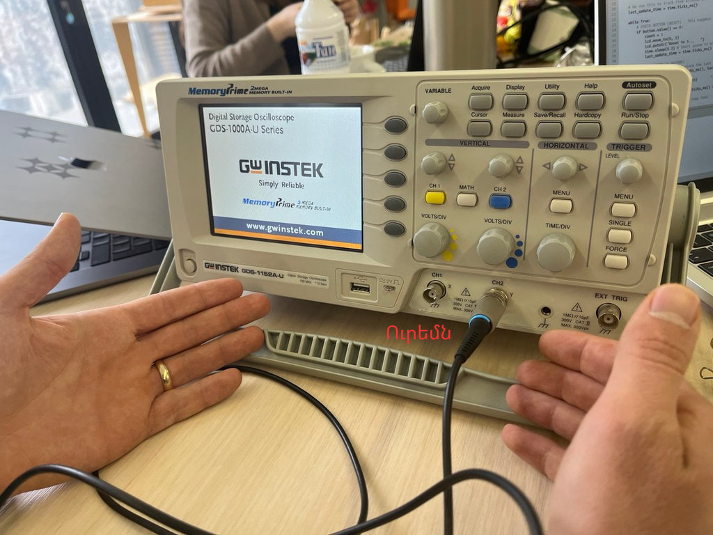
In our lab, we began the group assignment using the GW Instek GDS-1152A-U oscilloscope. This step is important for working with microcontrollers (MCUs) because an oscilloscope allows us to visualize electrical signals as voltage–time graphs, acting as the “eyes” for debugging embedded systems. While a multimeter provides static or averaged values, an oscilloscope shows the dynamic, real-time behavior of circuits, which is essential for detecting issues that occur within microseconds.
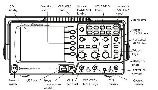
This model is part of the GDS-1000A-U series and is known for its durable and user-friendly design.
- MemoryPrime Technology: Maintains a high sampling rate (1 GSa/s) over longer time periods using a 2 Mega-point record length.
- Performance: 150 MHz bandwidth, 2 channels, and a 2.3 ns rise time.
- Display: 5.7-inch TFT color LCD with a resolution of 320 × 234.
- Connectivity: USB Host and Device ports for data logging and saving waveforms in formats such as CSV, JPEG, or video.
- Power: Supports universal 100–240 V AC input.
Panel Overview from this document
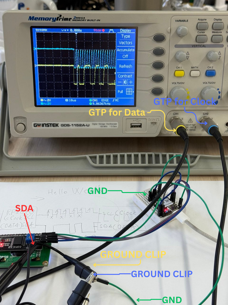
First, we wrote a simple program that generates a counter signal. After uploading the code, we connected the RP2040 to the oscilloscope: the GND pin was connected to the probe’s Ground Connector, and the signal pin (SDA) was connected to the probe’s Grabber. This allowed us to observe the signal behavior and measure the timing directly on the oscilloscope.
Below is the code used for the test.
import machine
import time
from pico_i2c_lcd import I2cLcd # Ensure this file is on your Pico
# I2C configuration
I2C_ADDR = 0x27 # Common address; use i2c.scan() to confirm
I2C_NUM_ROWS = 2
I2C_NUM_COLS = 16
# Initialize I2C (Bus 0, SDA=GP0, SCL=GP1)
i2c = machine.I2C(0, sda=machine.Pin(0), scl=machine.Pin(1), freq=400000)
lcd = I2cLcd(i2c, I2C_ADDR, I2C_NUM_ROWS, I2C_NUM_COLS)
counter = 0
while True:
lcd.clear()
lcd.putstr("Counter: " + str(counter)) # Print current count
print("Count:", counter)
counter += 1
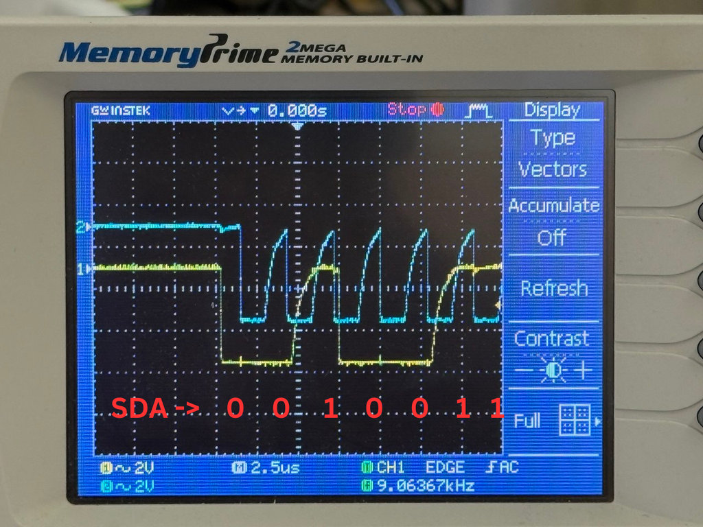
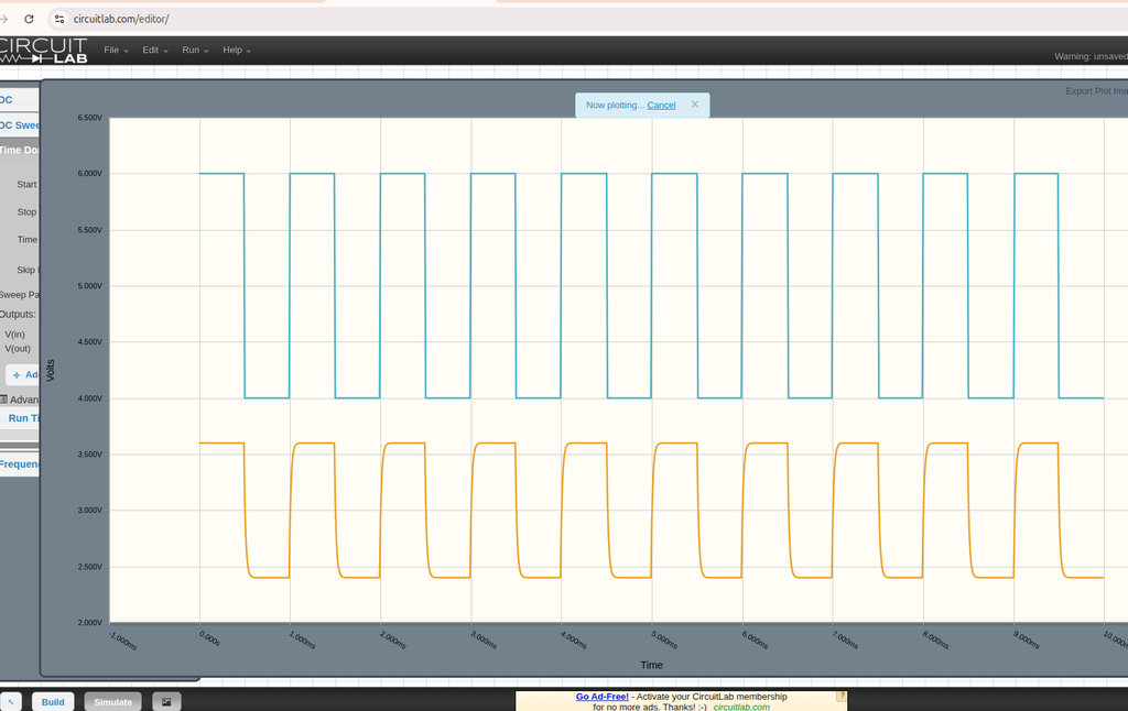
time.sleep(1) # Wait 1 secondThe image shows the I2C communication signals as captured on the oscilloscope. This is a digital signal used to transmit data between the RP2040 and the LCD.
The pulses represent two synchronized signals:
Yellow trace (CH1):This is theSDA (Serial Data)line, which carries the actual data bits.Blue trace (CH2):This is theSCL (Serial Clock)line. It acts like the “heartbeat” of the communication, telling the receiving device exactly when to read the data on the SDA line.
For example, the SDA data sequence (0 0 1 0 0 1 1) shows the binary interpretation of the pulses:
- Logic 1 when the SDA pulse is high
- Logic 0 when the SDA pulse is low
SDA data is only considered valid and “counted” as a bit when the SCL clock signal is high.
In the bottom right corner, the oscilloscope shows a frequency of approximately 9.06 kHz, which is the rate at which these clock pulses are activated.
We also tested the toggle test, which is a standard benchmark used to measure the maximum execution speed of a microcontroller’s software.
In MicroPython, each line of code (for example, led.toggle()) must be interpreted by the processor. This introduces overhead, which limits how fast a pin can physically change its state.
By toggling the pin as quickly as possible in a loop, we can measure the “raw” speed of the MicroPython interpreter on the RP2040.
from machine import Pin, Timer

# Setup GPIO 15 as output
led = Pin(15, Pin.OUT)

# Define the toggle function
def toggle_pin(timer):
    led.toggle()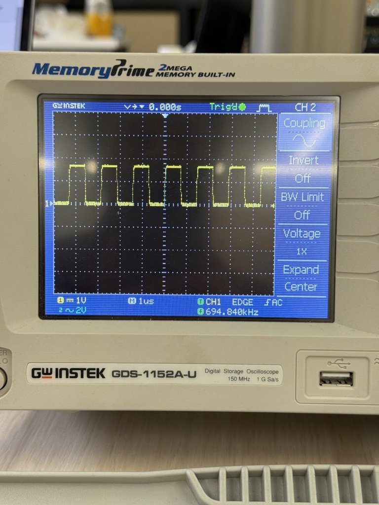
Hrach performed the same toggle tests using C++ instead of MicroPython and achieved a maximum toggle speed of 1.55 MHz.
This shows the difference in execution speed between interpreted MicroPython code and compiled C++ code on the RP2040.
You can see our group assignments page here.
PCB can be fabricated
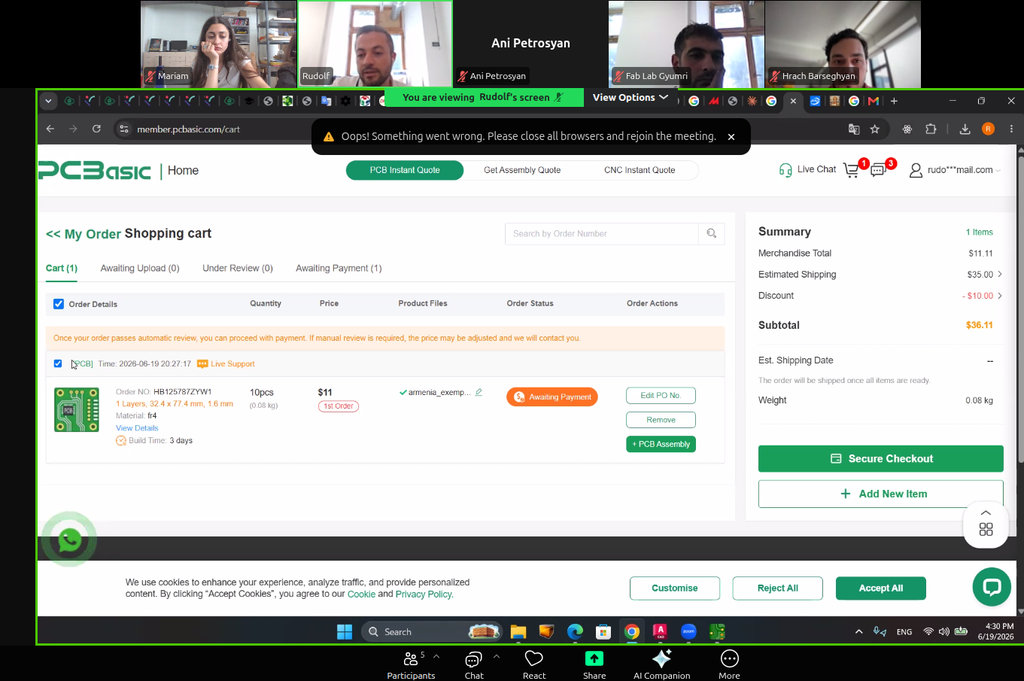
We also learned another very useful thing: instead of spending time and effort manufacturing our own PCBs, we can simply order them from a PCB manufacturer.
During a Zoom meeting, our instructor Rudolfs explained the entire ordering process in detail, and we used my car PCB as an example to learn the workflow.
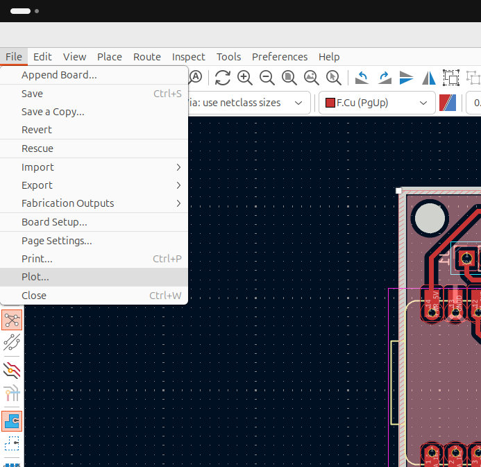
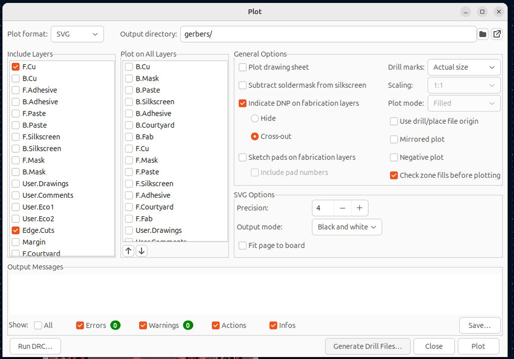
First, we open our PCB design in KiCad and select File → Plot...
In the window that opens, we choose the Output Directory. A small dialog appears where we click the folder icon and specify the folder name that will later be uploaded to the online PCB manufacturer.
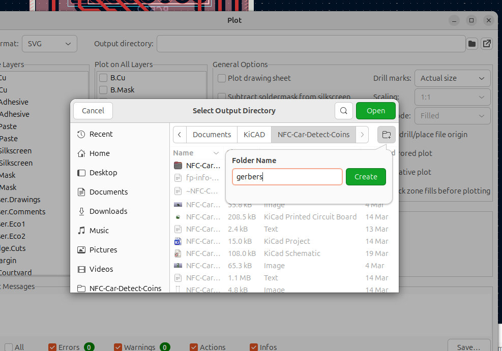
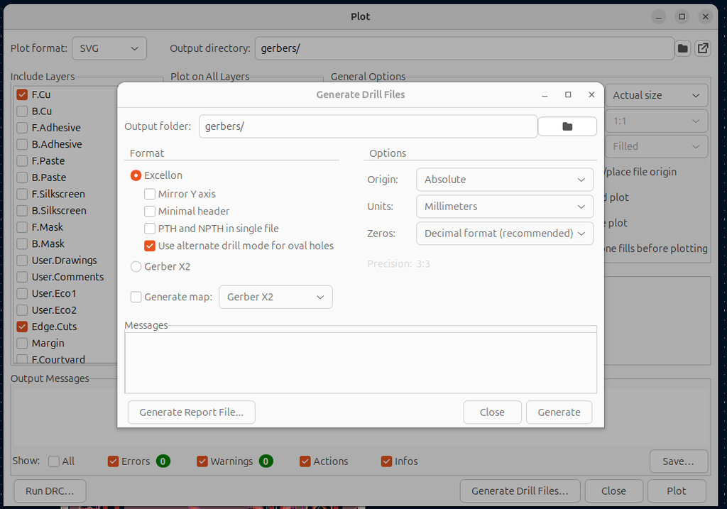
Next, we click Generate Drill Files..., make sure that the output folder is the one we selected, and then click Generate.
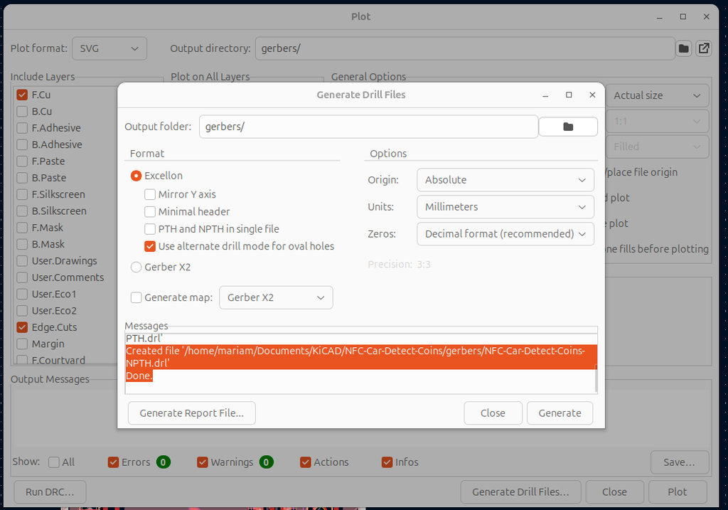
Another small window appears confirming that the .drl file has been successfully generated inside the Gerbers folder.
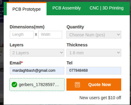
After that, we visit PCBasic.com, where we are going to order our PCB.
On the website, we first enter our contact information, such as our email address and phone number. Then we upload the Gerber files, which should first be compressed into a .zip archive. Finally, we click Quote Now.
If we did not specify the PCB dimensions earlier, we can enter them here in the Size section.
In the image below, I have highlighted the settings that are important when placing the order.
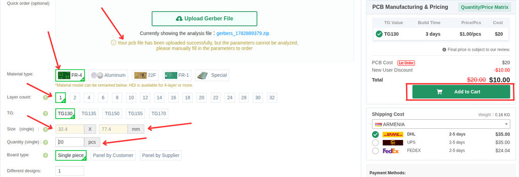
Based on my PCB, I plan to order 20 FR-4 single-layer PCBs, which will cost approximately $10.
simulate a circuit
For the individual assignment, I first decided to start with simulation experiments in order to better understand the physical principles of electronics. Simulations allow observing the behavior of a circuit before using real hardware.
Since my operating system is Ubuntu, I encountered some difficulties downloading and running LTspice. Because of that, I decided to use the CircuitLab online simulator, which allows building and testing electronic circuits directly in the browser without installing local software.
Using CircuitLab, I can easily create circuits, change component values, and observe the results. This approach helps me better understand the fundamentals of electronics before implementing the circuit in real hardware.
For the simulation assignment, I will build an example of a square wave circuit. This example allows demonstration of both time-domain analysis and frequency-domain analysis, which are fundamental concepts in electronics.
A square wave is mathematically composed of the sum of many sinusoidal waves (harmonics). A low-pass filter removes these high-frequency harmonics, transforming the sharp edges of the square wave into a rounded shape, or even into a pure sinusoidal wave if the filter is strong enough.
During the simulation, it is possible to observe how the capacitor charges and discharges over time. This behavior is fundamental for understanding how real electronic circuits process digital signals.
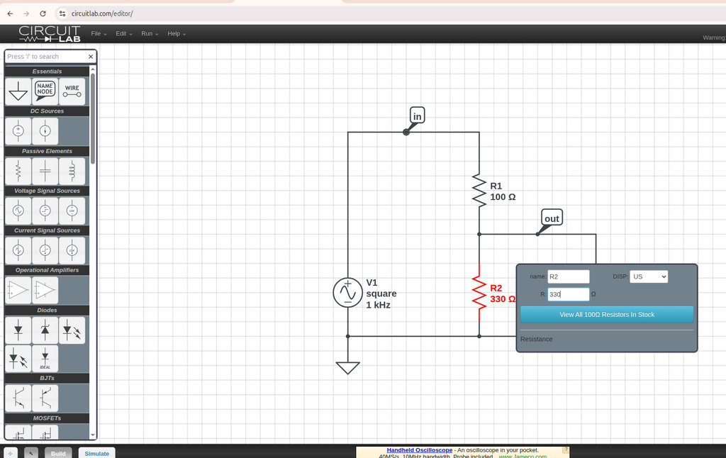
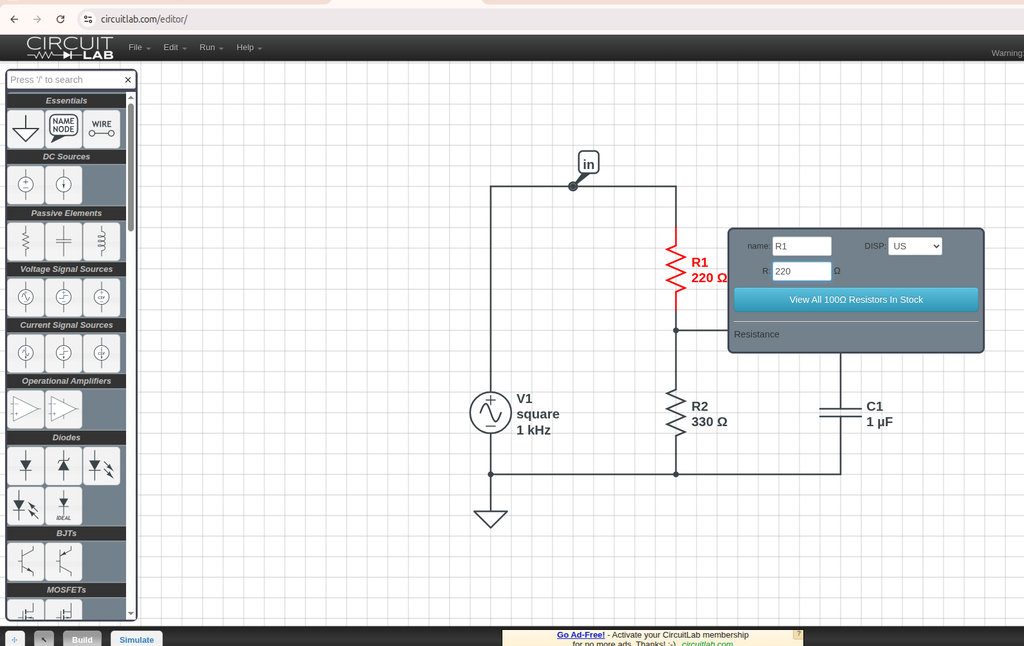
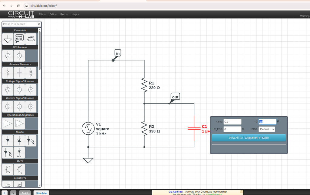
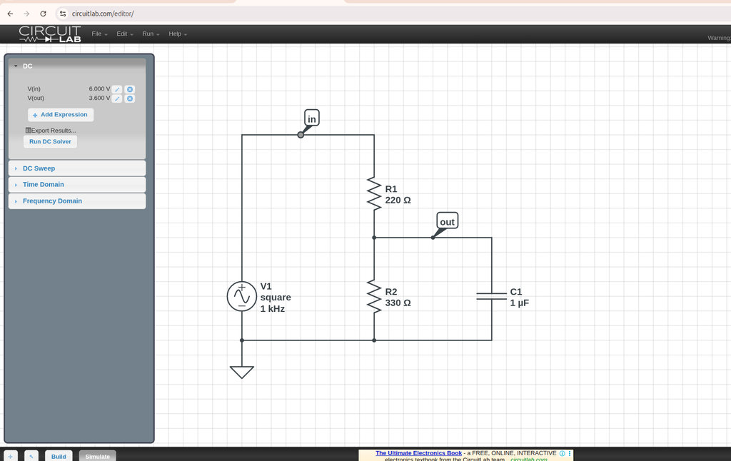
We are going to explore putting a square wave into a low pass filter as a quick getting started tutorial for circuit lab. When you start the editor, you are automatically in Build Mode. On the left, you'll see the Build Box, which has all the circuit elements you can use. We click on the voltage function generator, which is going to make our square wave. Then, we click somewhere on the grid to place it in our circuit. Now we'll add a couple of resistors. And I can drag these resistors around to place them where I want them. I added also capacitor. So to wire these elements up, you can just put your mouse over any of the terminals, and click and drag to extend a wire out to wherever you want.
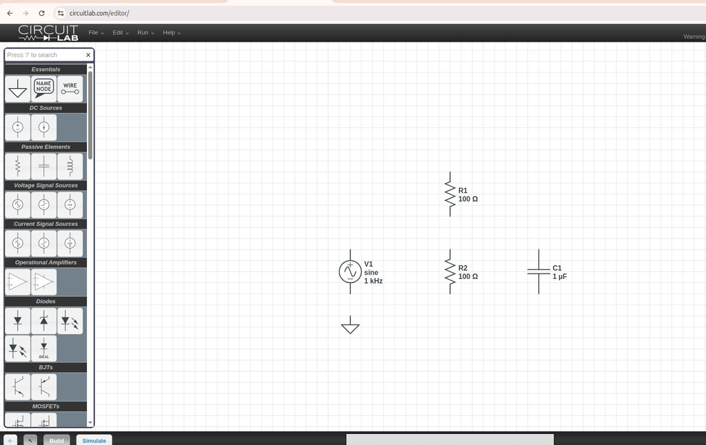
Now, I can double click the resistors to bring up the parameters and change their values. I set this one to 330 ohms, and R2 to 220 ohms, and set the capacitor to "1u". The "u" means micro, for 1 microFarad.
I can set up the voltage function generator's parameters too. We can set the DC offset to 5, leave the frequency at 1000 Hz, and make it a square wave.
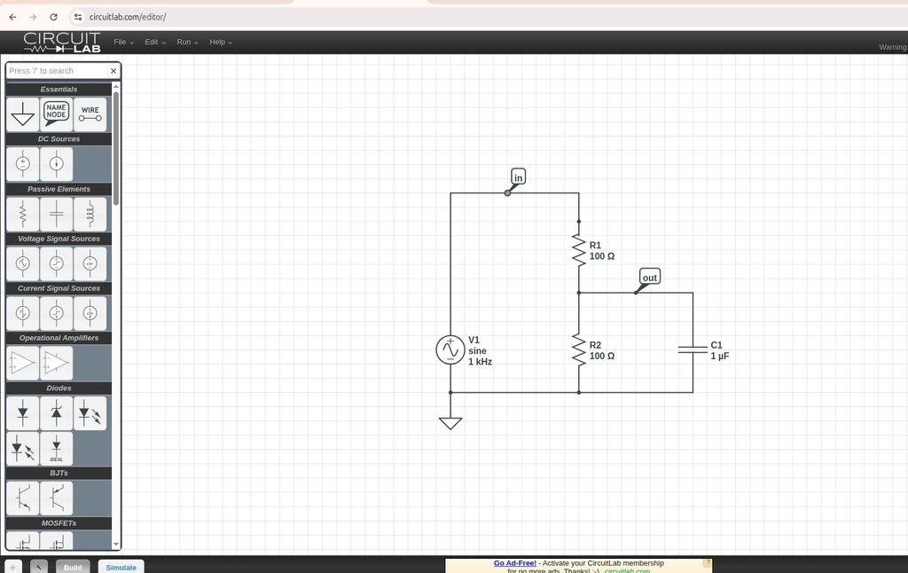
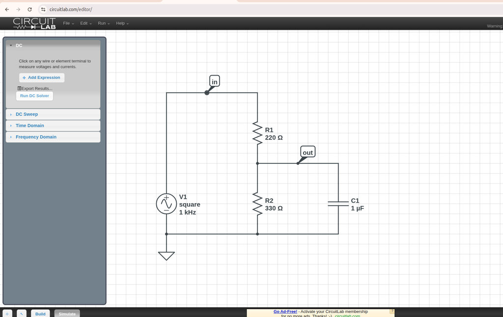
The circuits done so lets click “Simulate” here at the bottom. First, we see the DC simulation mode, and if I click "Run DC Solver", it tells us that the simulation is complete. Now, it says I can click any wire or terminal to track its value, so I'll click on "in" and "out" to track those voltages, and the calculated voltages appear.
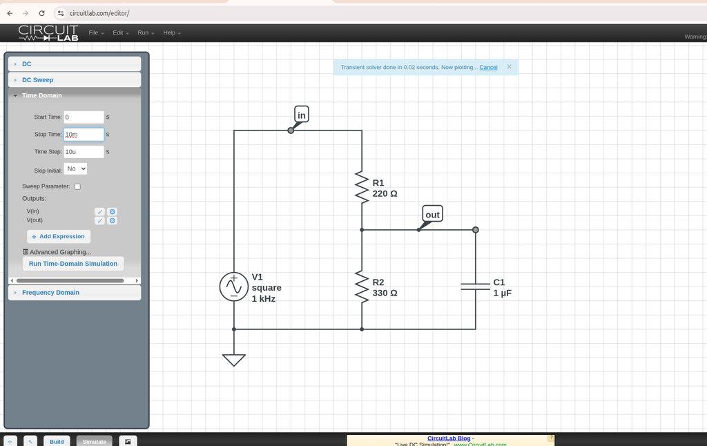
Now let's run a time simulation and see the square waves. First we've got to tell it how long to run a simulation for. We had a 1000 Hz square wave, which is a1 millisecond period, so let's simulate for 10 milliseconds so we can see several cycles. Just type "10m" into the box, and it knows that little "m" means milli. We have to pick a simulation timestep, and a good start would be to simulate for 1/1000 of the total simulation run, so just type "10u" with "u" for micro. Now we again pick what outputs to plot, so we click "in" and "out", and you see it adds those to the outputs list. Then we click "Run time-domain simulation", and in just a second, we get a plot.
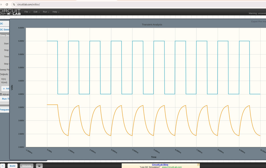
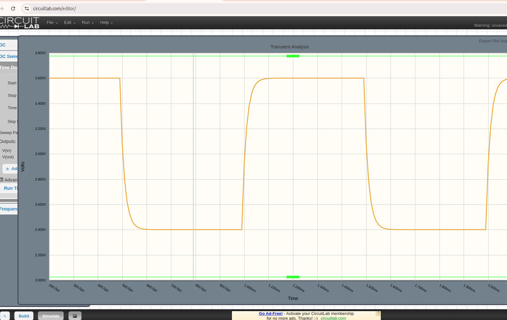
🔵 Blue Signal — Input Voltage (V(in))
- This is the square wave generated by the source V1.
- It is the signal labeled “in”
- Frequency: 1 kHz
- Voltage levels: about 4 V – 6 V.
- This signal goes directly into the resistor network (R1 and R2).
🟠 Orange Signal — Output Voltage (V(out))
- This signal is measured at the node labeled “out”.
- It is the point between R1 and R2, where the capacitor C1 is connected to ground.
- The capacitor smooths the signal, so the waveform edges are rounded instead of sharp.
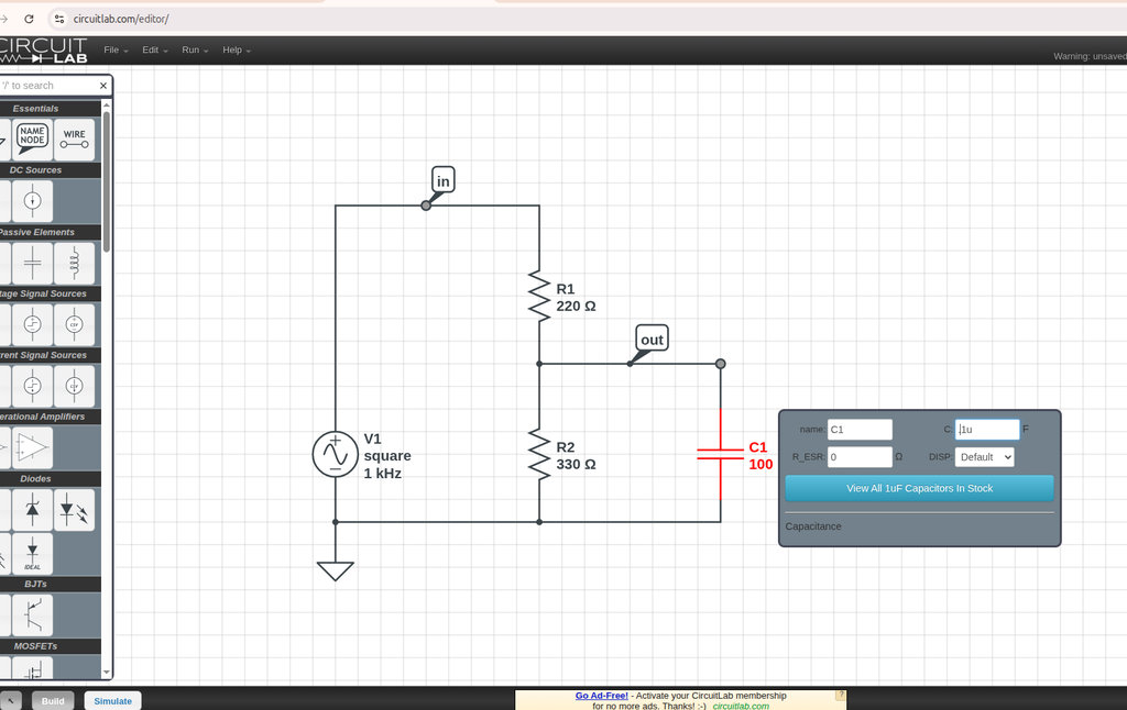
Now, we get a lot of the exponential RC behavior here, so let's try changing the capacitor size to see what happens. We click "Build", then double click the capacitor, and change it to ".1u". Back to simulate, then "Run time-domain simulation", and now we see a lot more square-looking output signal.
To get a close-up view we can drag on the graph to zoom in.
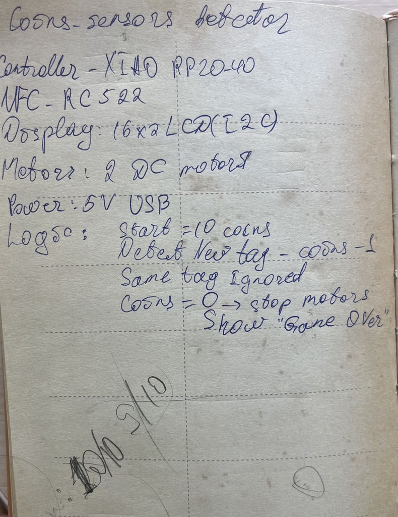
Final Project – Coin Collection System (PCB Planning)
Now it is time to implement another important part of my final project — the coin collection system for the car-robot.
The goal is:- Detect coins placed on the game board using
NFC tags - Count collected coins
- Display the total number on an
I2C LCD
To make the system compact and reliable, I will design a custom PCB where all components are properly arranged and electrically connected.
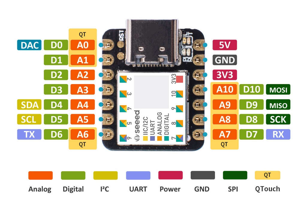
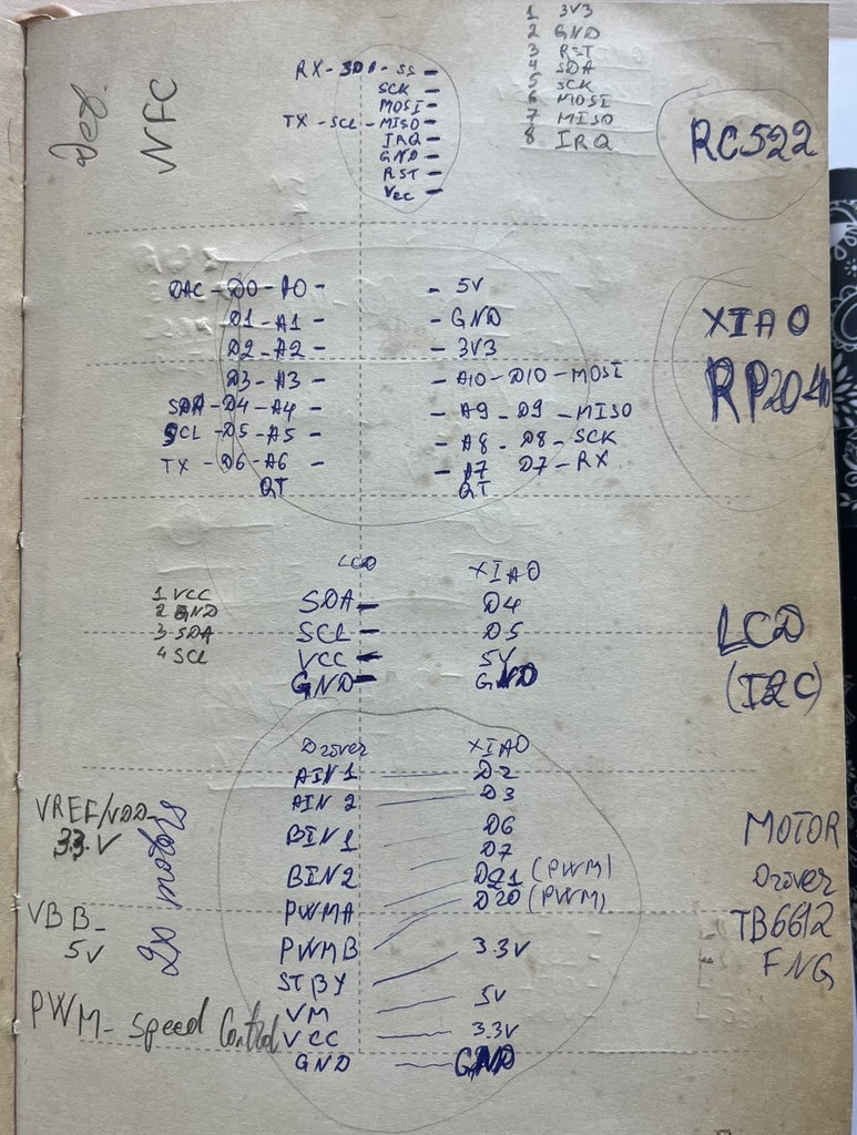
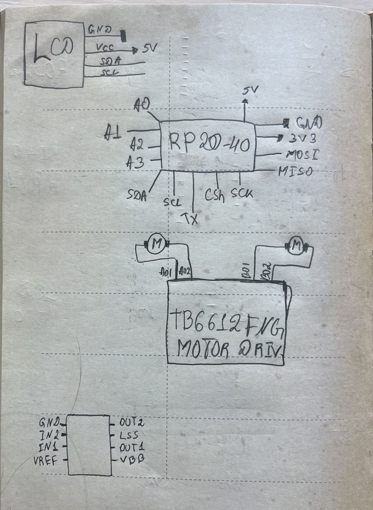
The main controller of the system is the RP2040.
I chose this microcontroller because the robot needs to handle multiple tasks simultaneously:
- Read NFC tags (
MFRC522 RC522 NFC reader) - Control two motors (
A4953) - Update the LCD display (
I2C) - Process coin counting and game logic(
Seeed Studio XIAO RP2040)
Additionally, RP2040 is available in our FabLab and provides enough performance, GPIO pins, and flexibility for this multi-task system.
To implement the coin detection, I decided to use an NFC-based system.
Components:
NXP Semiconductors MFRC522 NFC ReaderNFC tags placed inside or under each coin
Each NFC tag has a unique UID (Unique Identifier). This allows the robot to:
- Detect when a coin is collected
- Identify which specific coin was detected
- Avoid counting the same coin multiple times
The system already uses several peripherals:
- NFC reader (
MFRC522) - Two motor drivers (
A4953) - Control logic
To save pins and PCB space, I selected an I2C LCD.
Advantages:
- Uses only 2 signal lines (
SDA,SCL) - Reduces wiring complexity
- Ideal for compact PCB design
- Leaves more GPIOs available for motors and other modules
The LCD will display:
- Number of collected coins
- Game status information
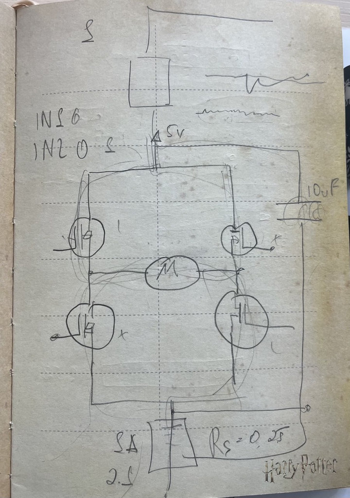
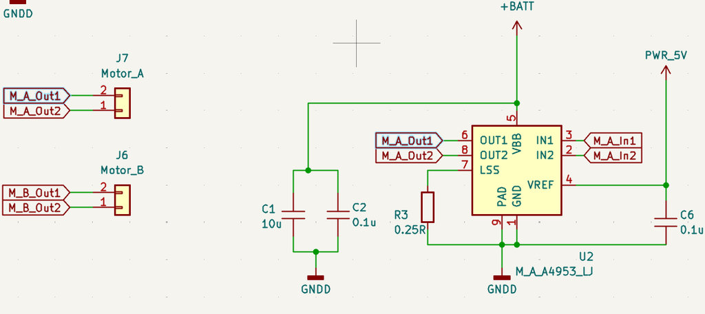
Two DC motors are used to enable differential drive movement. By controlling the left (Motor_A) and right (Motor_B) wheels independently through the Allegro Microsystems A4953 drivers and the Raspberry Pi Foundation RP2040, the robot can move forward, turn left or right, rotate, and stop accurately. This allows precise navigation and positioning when detecting NFC tags.
Two Allegro Microsystems A4953 motor drivers are used to control Motor_A and Motor_B independently. The Raspberry Pi Foundation RP2040 cannot drive motors directly because motors require higher current and voltage. Each A4953 provides an H-bridge for direction and speed control, protects the microcontroller from motor noise, and enables differential movement of the robot.
KiCad Introduction
To design the PCB, I became familiar with another open-source tool — KiCad, which allows designing and modeling electronic devices.
KiCad is a free and open-source Electronic Design Automation (EDA) software used for schematic capture and PCB layout.
Software download: https://www.kicad.org/download/
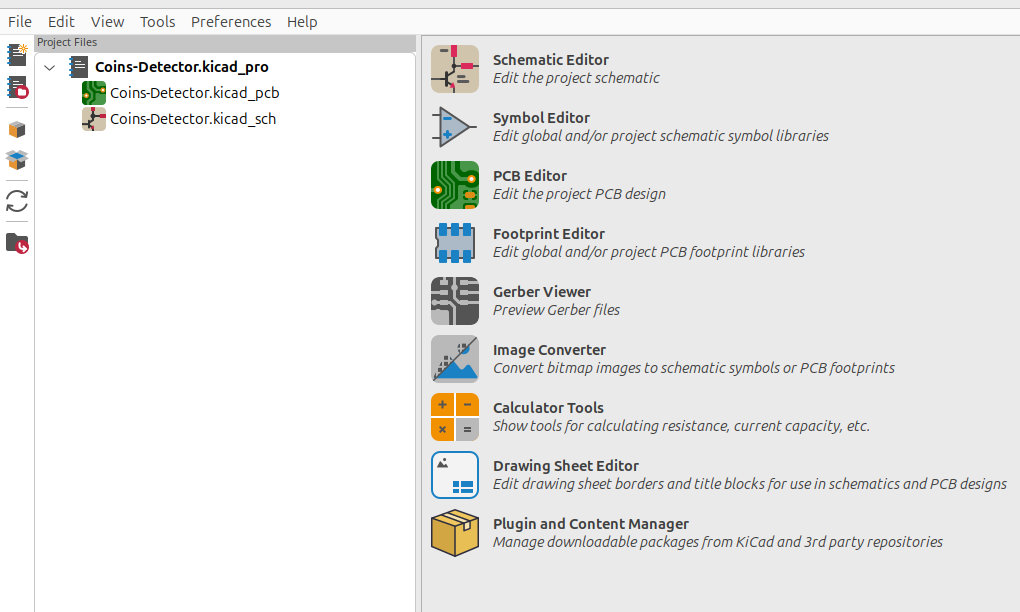
First, I will share with images the process of creating a new project in KiCad.
Then it is necessary to start working from the created kicad_sch file. It is important to understand which components are needed and add them in this workspace.
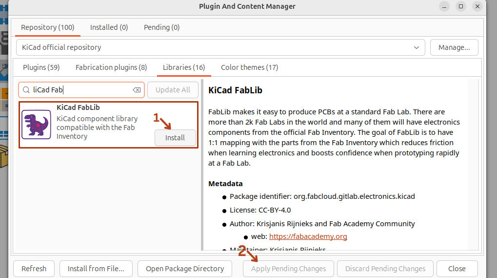
First, I need to import the Fab KiCad library, which is a standardized collection of electronic components specifically related to the official Fab Inventory used in Fab Labs around the world.
The symbols are already linked to parts commonly available in Fab Labs, which reduces assignment mistakes.
It is optimized for surface-mount devices (SMD) and digital fabrication (for example, PCB milling).
Thanks to the author.
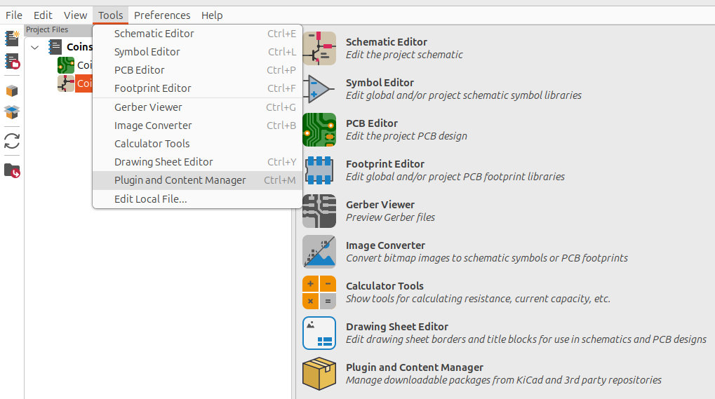
We open Tools > Plugin and Content Manager, select the Libraries tab, search for "KiCad FabLib", click Install, and then Apply Pending Changes.
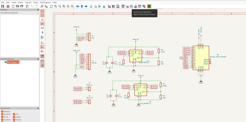
Now in kicad_sch we can add the required components.
First, from Place, we select Place Symbols, and in the opened window we search for RP2040 and from the fab-kicad subsection select it.
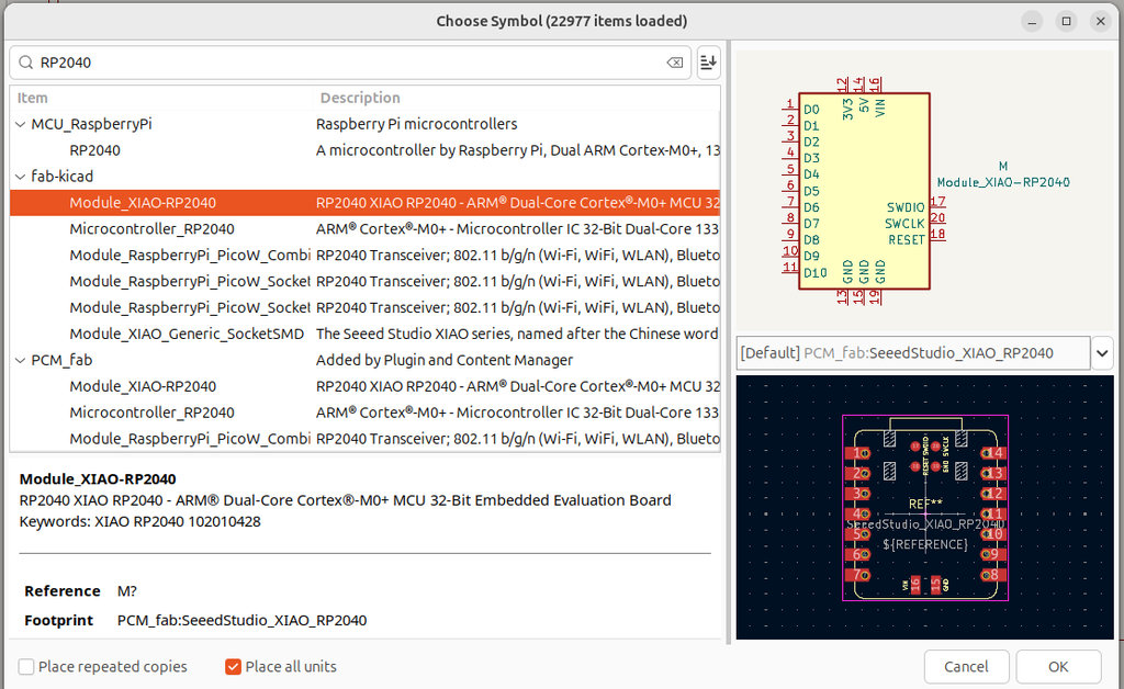
Then again from Place we select Place Symbols, or simply press the letter A, and again we see the search window.
I search for the required components and place them in the workspace.
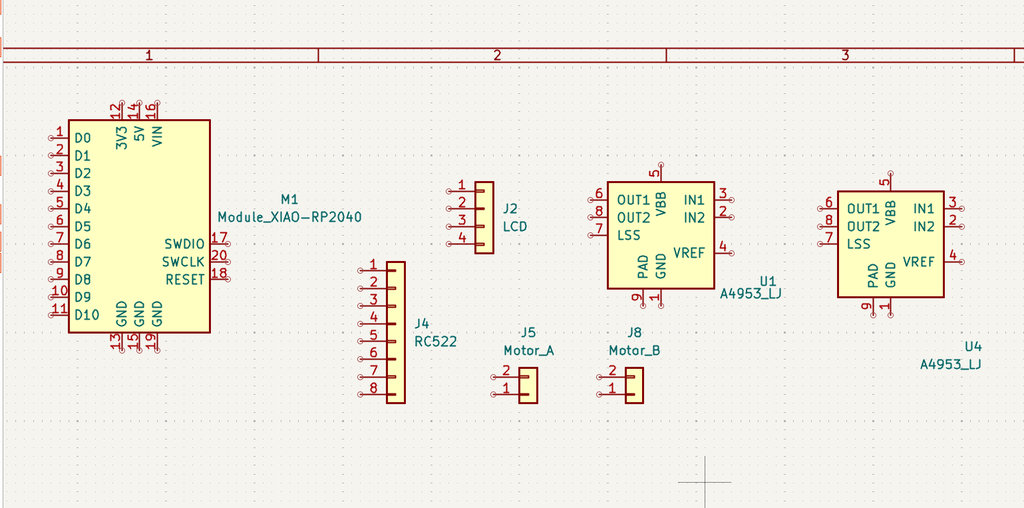
For each component, I searched for and studied the corresponding documentation to understand what connections are required.
For example, I studied the Rc522 Datasheet to understand which pins are available and what connections are required.
The I2C_1602_LCD Datasheet was already familiar to me, but to deepen my knowledge, I reviewed it again.
From the A4952-3 Datasheet, I extracted the necessary information and understood that capacitors and resistors are also required.
The resistor is used to control and limit the current flowing through the motor in order to prevent damage and ensure precise control.
Current regulation: The Allegro A4953 uses a low-value external sense resistor connected between the LSS pin and ground. When the voltage reaches the threshold value, the internal PWM circuitry “cuts” the current to keep it at a safe and stable level.
Capacitors are used to maintain stable power supply and to filter electrical noise generated by the motor.
Voltage stability: A large electrolytic capacitor (typically 1000μF) is placed on the VBB (Load Supply) pin to regulate large current fluctuations during motor startup or direction changes.
Noise filtering: A smaller ceramic capacitor (often 0.1 µF) is placed as close as possible to the integrated circuit to filter high-frequency noise and prevent motor resets or unstable behavior.
These are my notes taken while reading the documentation.
And here, after placing the pins:
For example, to assign a value to the capacitor I placed, I simply double-click on it and enter the appropriate value in the Value field.
In this screenshot, I also show that by giving the pins the same name using the Place Global Labels tool (or simply pressing Ctrl + L), it becomes much easier to route the connections later in the PCB Editor, since the corresponding nets are automatically identified.
Then I click “Switch to PCB Editor” in order to transfer all these components into the PCB Editor environment.
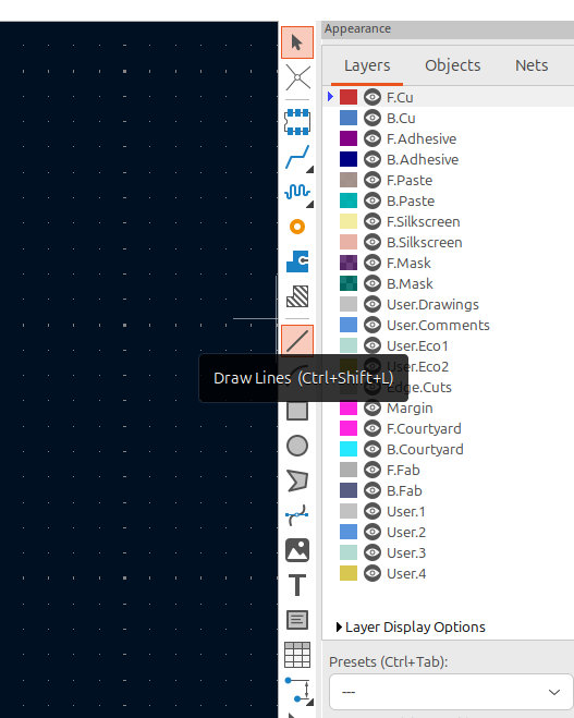
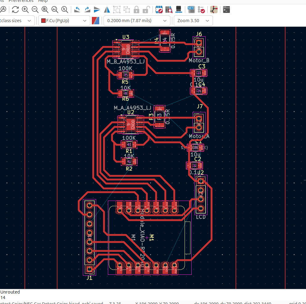
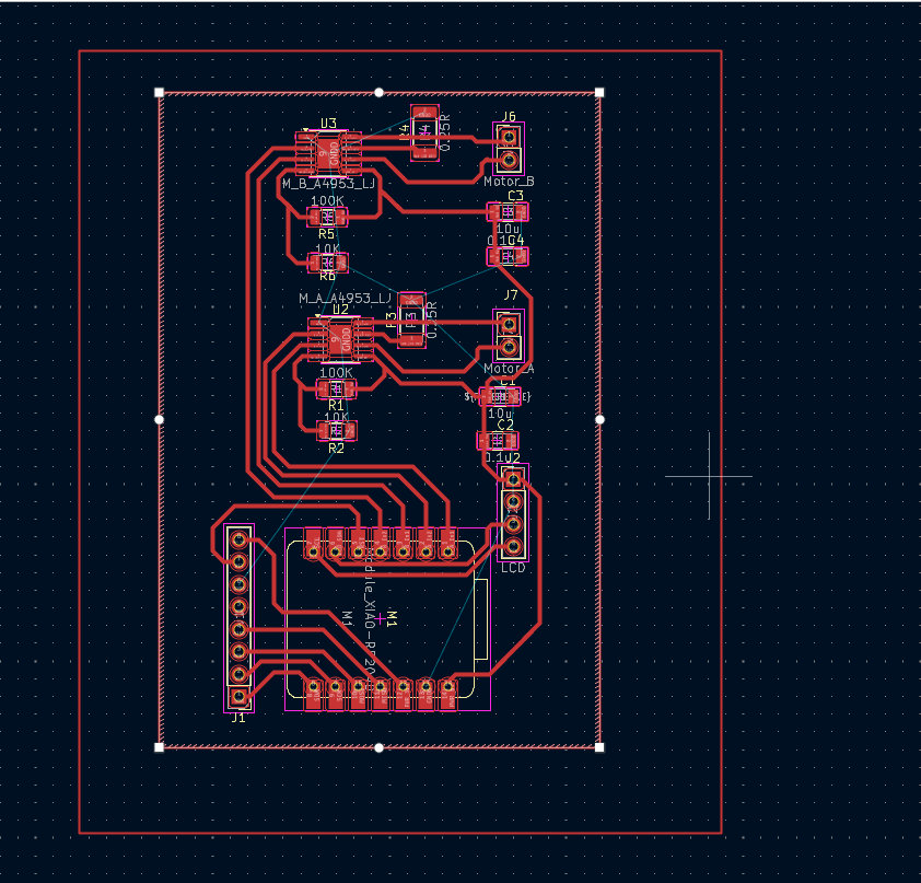
After switching to the PCB Editor, it is necessary to connect all the corresponding pins together. For that, I use the Draw Lines tool to connect all the required pins.
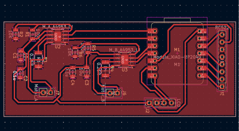
Here is the final result.
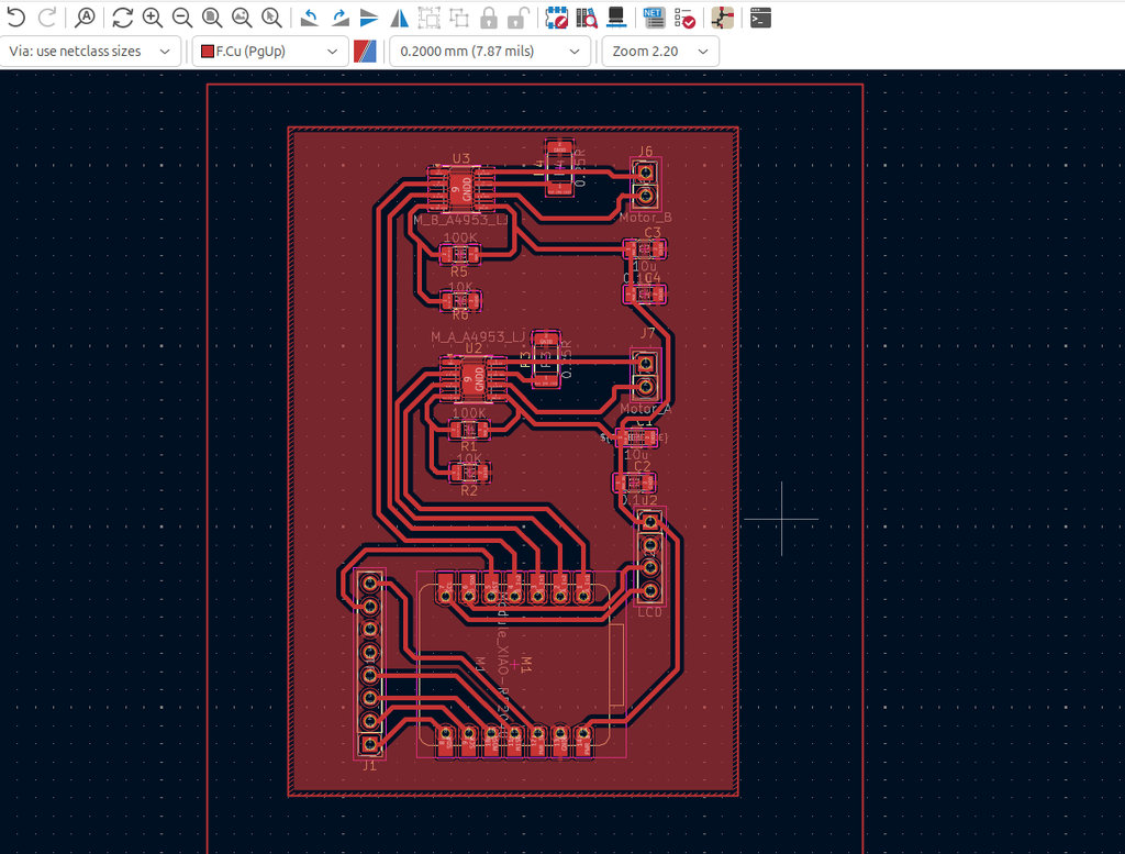
Next, using the Draw Filled Zones tool, I need to make the entire PCB area connected to GND. By selecting the net that should be GND, the PCB looks like this.
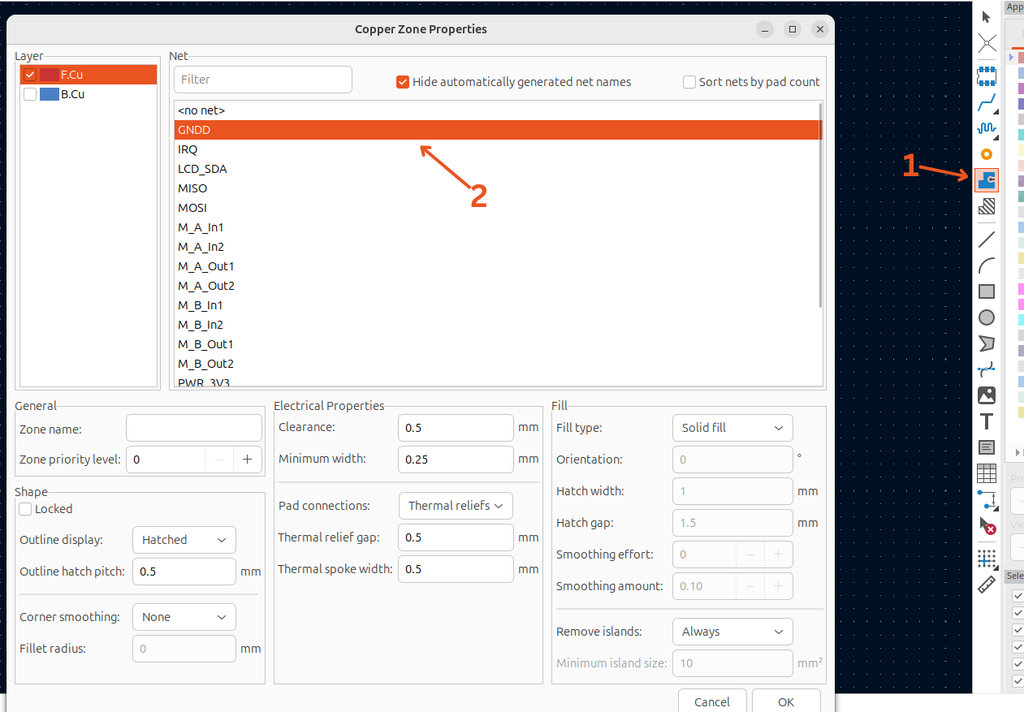
Then I press B to fill the entire area with GND.
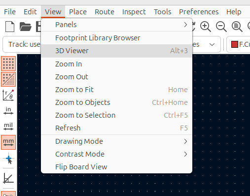
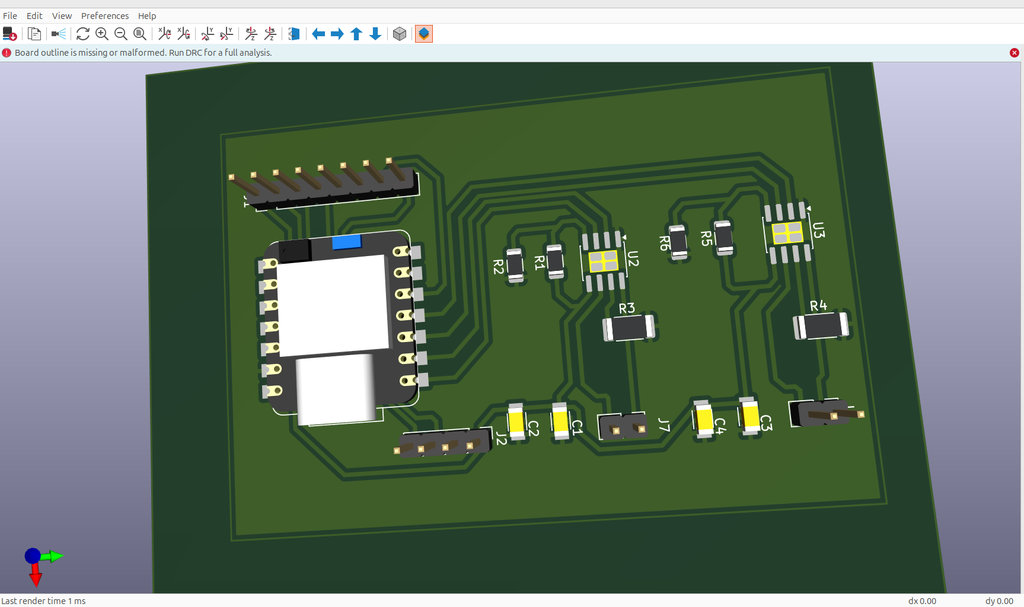
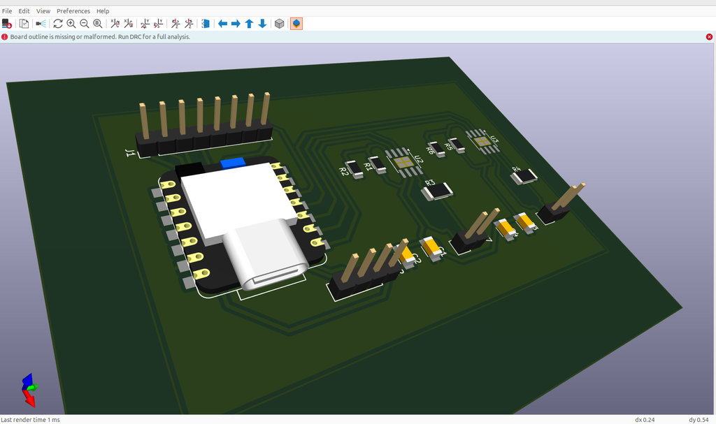
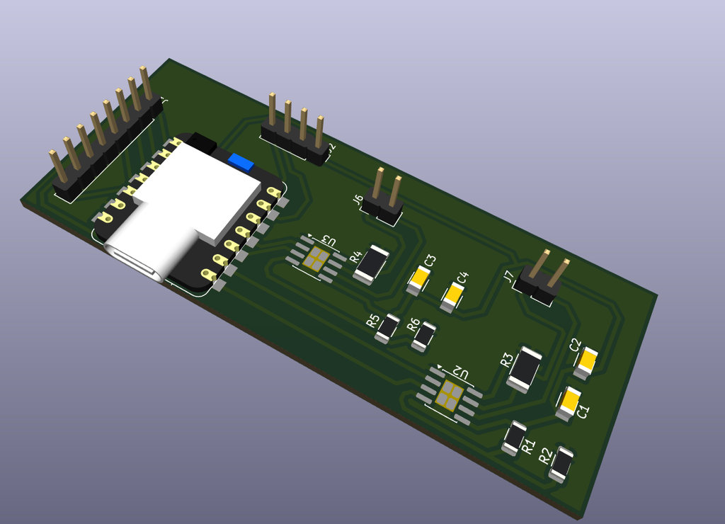
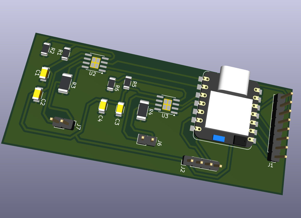
By clicking View 3D Viewer, we can see our PCB in a 3D view..
Here is the final result.
Design Rule Check (DRC)
DRC is an automated and often real-time validation process in PCB design software that checks the layout against physical and electrical constraints. It prevents manufacturing failures such as short circuits and trace violations by applying design rules like clearances, trace widths, and hole sizes before production.
For this reason, it is necessary to go through this step to ensure that my PCB is fully ready for fabrication.
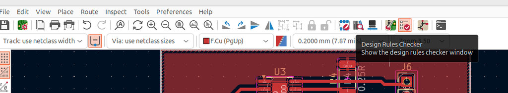
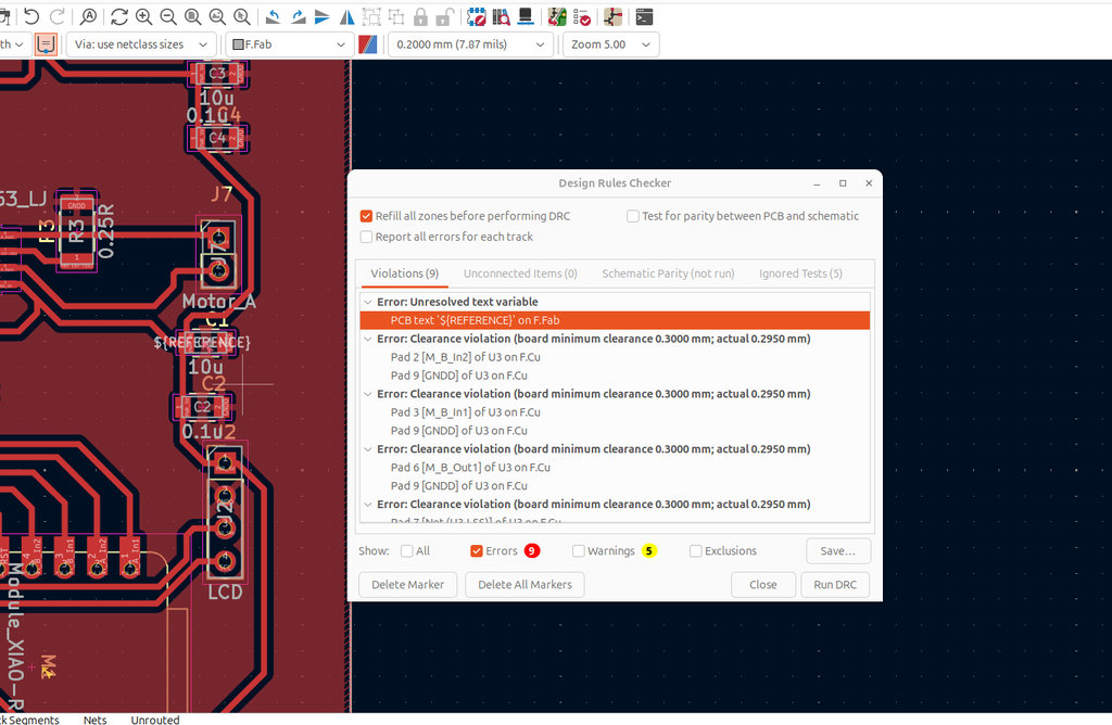
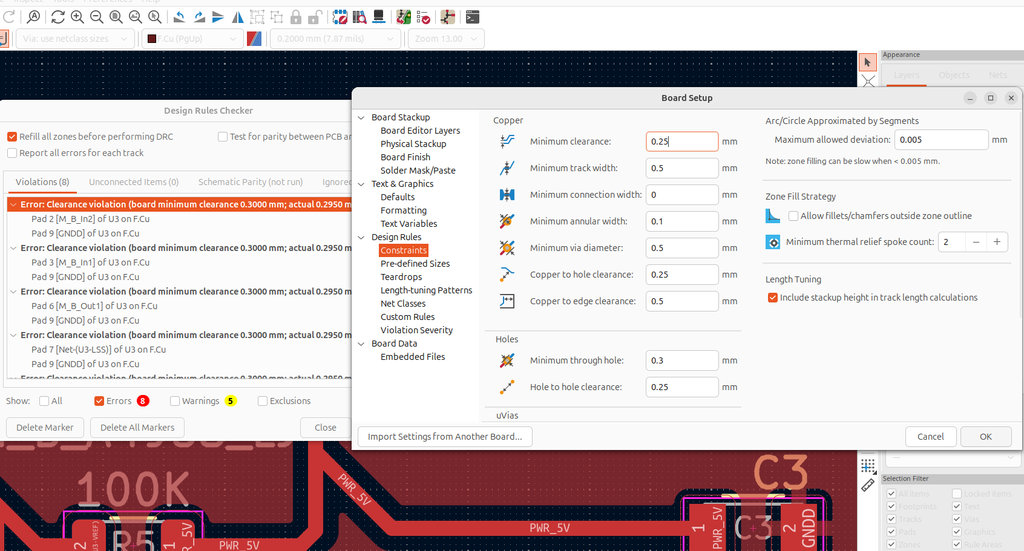
To do that, I open the DRC window using the Design Rules checker.
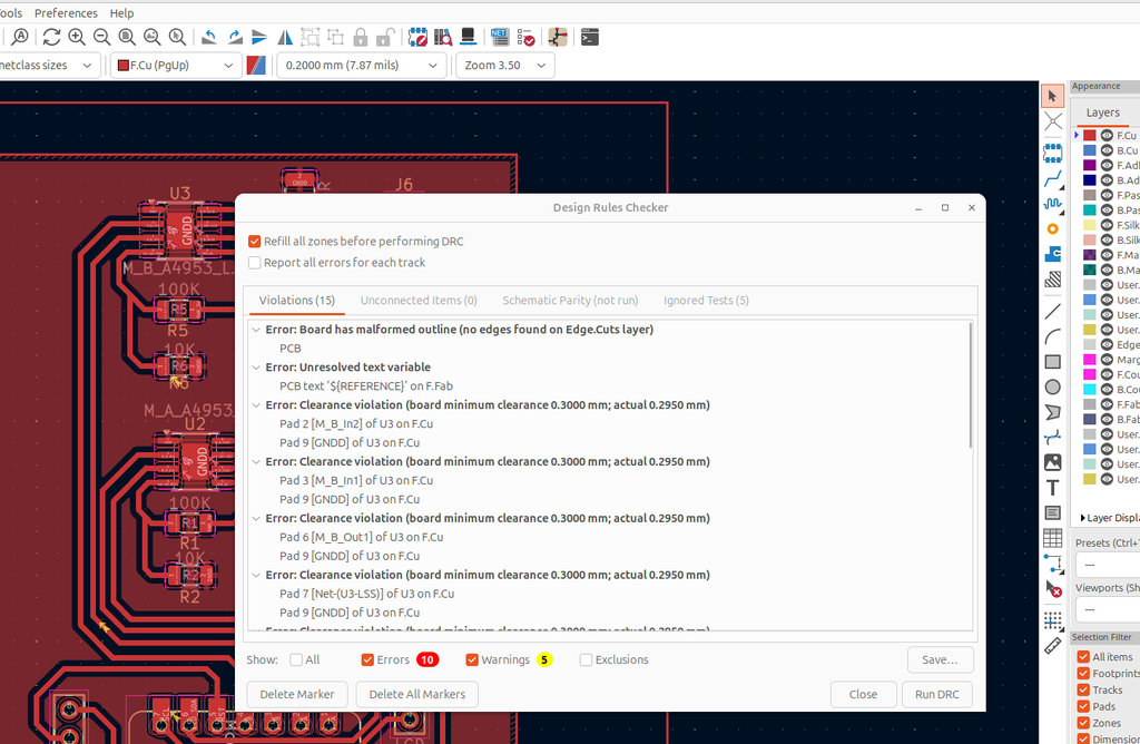
Here I can see that I have 10 errors. The warnings can be ignored because they are not critical issues and do not affect the PCB milling process.
The first error is: "Board has malformed outline (no edges found on Edge.Cuts layer)"
This error means that the Design Rule Checker (DRC) cannot identify a valid, continuous board outline. For the outline to be valid, it must be a closed shape without gaps, overlaps, or self-intersections on the Edge.Cuts layer.
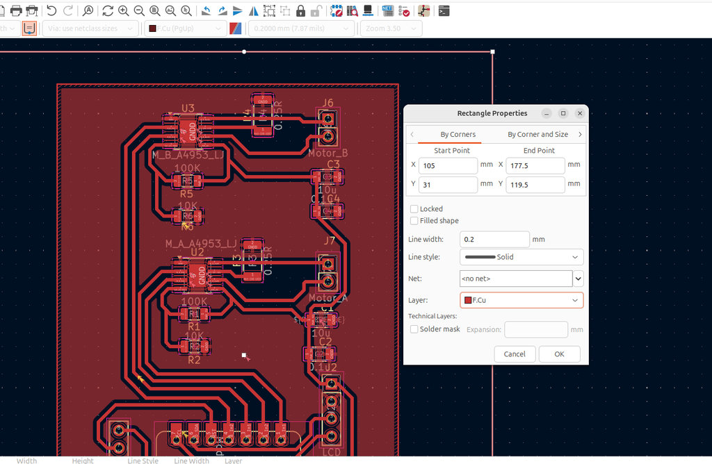
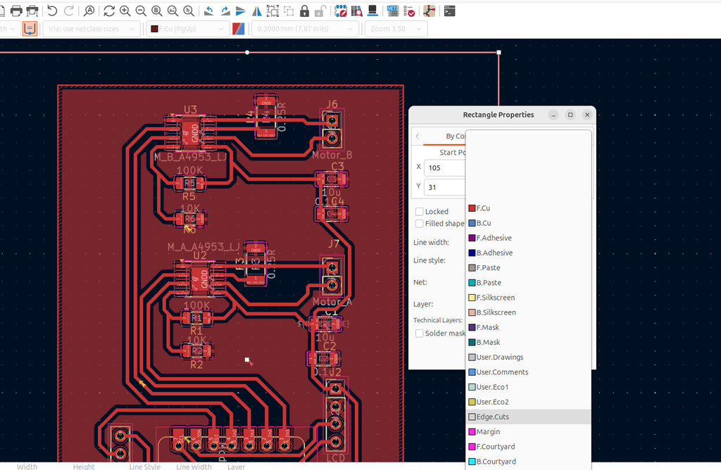
Since I do not have open boundaries in my design, I checked the layer type. It should be set to Edge.Cuts, but in my case it was mistakenly set to F.Cu. After correcting the layer type, the issue was resolved.
Then I noticed that the text ${REFERENCE} appeared on the capacitor footprint. After confirming that I did not need it, I simply deleted it.
Next, when I saw the "Clearance Violation" message, I opened the Board Setup window again. In the Constraints section, I set:
Minimum clearance to 0.25 mmMinimum track width to 0.5 mm
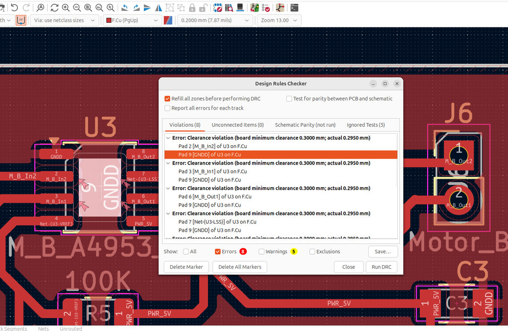
After running Run DRC again, I saw 0 errors.
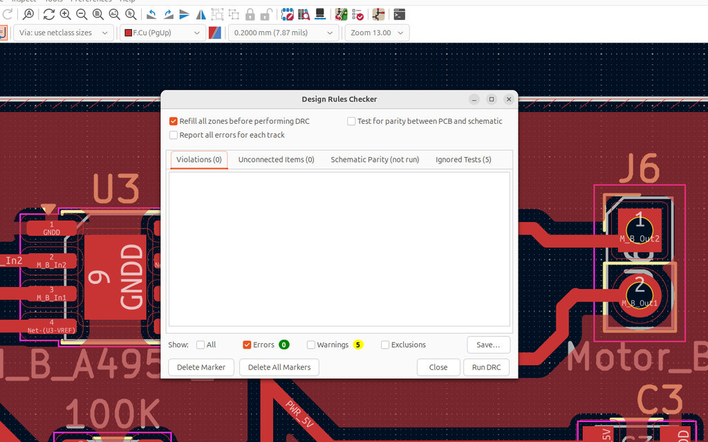
Therefore, everything is correct and the PCB is ready for milling.
However, during yesterday’s Regional Review, Jani mentioned a few design improvements. I implemented those suggestions today, and now the PCB looks cleaner and more organized. Thank you, Jani!
This week I designed the electronics and PCB for my final project. I defined the system architecture for the car-robot coin collection system and selected components such as the RP2040, NFC reader, motor drivers, and I2C LCD. After studying the datasheets, I created the schematic in KiCad and then routed the PCB in the PCB Editor with a GND filled zone. I enjoyed working with KiCad and seeing the hardware system come together. The most challenging part was carefully reading datasheets and ensuring correct connections and power design. This week I learned how to move from schematic design to a real PCB layout.
Individual assignment

AI prompt:
“And another image when she finished week 6.”