11. Networking and Communications
Summary
This week we communicated multiple devices using communication protocols and our custom PCBs. For our group assignment, we established communications and sent a message between two projects.
1. Introduction to Networking and Communications
In the realm of embedded systems and digital fabrication, networking and communications form the foundational infrastructure for enabling coordinated behavior among multiple electronic systems. At its essence, we apply this field to examine methodologies for reliable data transmission between computational nodes under specific requirements.
A network is a system of interconnected components designed to exchange information, resources, or control signals. In electronics and computing, networks enable a variety of devices, such as microcontrollers, sensors, or computers, to collaborate towards the same objectives, transforming isolated hardware into cohesive, intelligent systems.
Networking and communications technologies allow electronic systems to operate in conjunction, granting us with fundamental capabilities critical to modern digital fabrication and IoT ecosystems, such as;
- Distributed Computation - Divides workloads across specialized nodes, allowing us to offload intensive tasks to more capable devices.
- Real-Time Coordination - Enables precise timing across devices, allowing immediate feedback between sensors and actuators.
- Data Aggregation and Decision Making - Local preprocessing before cloud transmission, allowing us to collect sensor data for machine learning or analytics in an efficient manner.
- Scalable System Architecture - Modular designs with swappable components and redundant communication paths.
2. Communication Protocols
Communication protocols serve as the language that allows electronic devices to exchange data with precision and reliability. These protocols define the electrical characteristics of signals, and the logical rules that determine how devices initiate, maintain, and terminate conversations.
Protocols are generally divided into two main categories: wired and wireless. Each has its strengths and use cases, which we'll explore below.
2.1 Wired Communication Protocols
Wired communication protocols form the backbone of reliable, short-to-medium range data exchange in electronics. Unlike wireless systems, they are less prone to interference, offer better data integrity, and often consume less power. This makes them particularly suitable for embedded systems, digital fabrication tools, and sensor-based networks.
2.1.1 Synchronous Serial Protocols
Synchronous protocols rely on a shared clock signal to coordinate data transmission between devices. This allows for faster communication and better timing accuracy, though it often requires additional wiring for the clock line.
- I²C (Inter-Integrated Circuit) - A two-wire protocol (SDA and SCL) designed for short-distance communication between multiple devices. It supports multiple secondary (formerly "slave") devices on a single bus, with each identified by a unique address. Ideal for low-speed sensors, EEPROMs, and real-time clocks.
- SPI (Serial Peripheral Interface) - A high-speed, full-duplex protocol using four wires (MISO, MOSI, SCLK, and SS/CS). SPI is excellent for applications requiring fast data transfer, such as memory cards, displays, and ADC/DACs.
Asynchronous protocols do not rely on a shared clock. Instead, we program the devices to share timing conventions such as baud rate, and use start/stop bits to frame data. These are simpler to implement and require fewer wires.
- UART (Universal Asynchronous Receiver/Transmitter) - Common in microcontroller communication. It uses two lines (TX and RX) to transmit and receive data. Perfect for debugging and communicating a variety of modules with our microcontroller.
- RS-485 - This protocol is designed to send data reliably over long distances, even in noisy environments like factories or outdoor installations, making it powerful for industrial applications.
2.2 Wireless Communication Protocols
Wireless protocols remove the need for physical connections, enabling flexible and scalable device interconnection. While they are more complex and consume considerable power, they are ideal for distributed systems, mobile applications, and IoT environments.
- Wi-Fi - Offers high data throughput and internet access capabilities. Frequently used with ESP32 microcontrollers in IoT projects.
- Bluetooth - Suited for low power, short range communications. Good for wearable devices and interfaces.
- LoRa - Long-range, low power protocol ideal for sensor networks spread across large areas with minimal data needs.
- ZigBee - Mesh capable, low power wireless protocol often used automation and industrial monitoring.
3. I²C Protocol
The Inter-Integrated Circuit protocol is a synchronous, multi-master, multi-device serial communication protocol widely used in embedded systems. Developed by Philips Semiconductor in the 1980s, I²C allows multiple chips to communicate over just two wires, making it especially useful in compact and resource constrained environments.
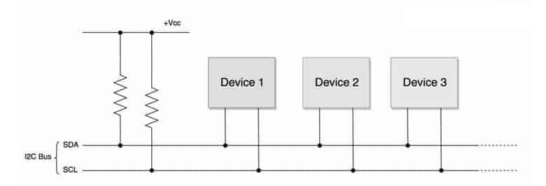
3.1 Physical Layer
I²C operates over two bidirectional lines:
- SDA (Serial Data) - Transmits the actual data between devices.
- SCL (Serial Clock) - Carries the clock signal generated by our main device.
3.2 Architecture and Addressing
An I²C bus typically consists of one "main" device (formerly called "master") and one or more "secondary" devices (formerly "slaves"). The main device initiates all communication and controls the clock signal. Each secondary has a unique 7 bit address, with support for optional 10 bit addressing.
Data is exchanged in packets, with the main device sending the address of the intended secondary, followed by read/write instructions and the data itself.
3.3 PROs
- Only two wires needed regardless of the number of devices.
- Support for multiple devices on a single bus.
- Synchronous timing simplifies the data handling.
- Well supported in microcontroller libraries and platforms.
3.4 CONs
- Short range communications, usually under 1 meter.
- Relatively slow compared to protocols like SPI.
- Limited by the number of available unique addresses.
4. My Communications System
For this week's assignment, I designed and built a custom communication system based on the I²C protocol, connecting three XIAO RP2040, one as the main node and two as secondary nodes. This system demonstrates simple wired communications using buttons and LEDs across the devices, coordinated by the central controller.
4.1 Physical Setup
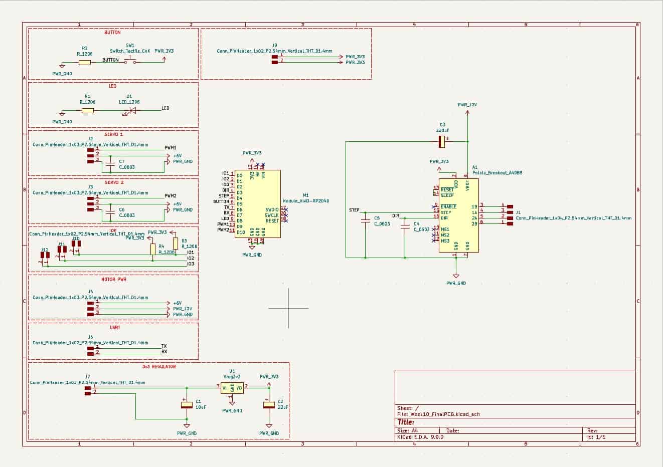
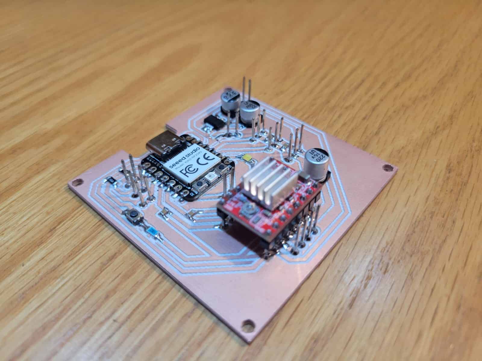
The system is built around my custom-designed XIAO RP2040 PCBs. My first, "V1" board, was developed during week 8, electronics production, while the second, "V2" board, was developed during week 10, output devices.
The leasons learned during previous assignments have culminated in the new "V3" version specifically designed with I²C communications in mind.
The main characteristics of the V3 development board that differ from V1 and V2 are:
- Dedicated I²C pins (SDA and SCL).
- Integrated 4.7 kΩ pull-up resistors on both lines to ensure correct bus behavior without needing external components.
The schematic is very similar to V2's, with the main difference being the use of dual pin headers for the I/O pins, and the addition of the 4.7 kΩ pull-up resistors placed on two of these I/O lines for I²C communications.
The other addition was a dual pin header to output 3.3V in case I needed to feed the other PCBs from V3. All other components have the same values and placement as V2's.
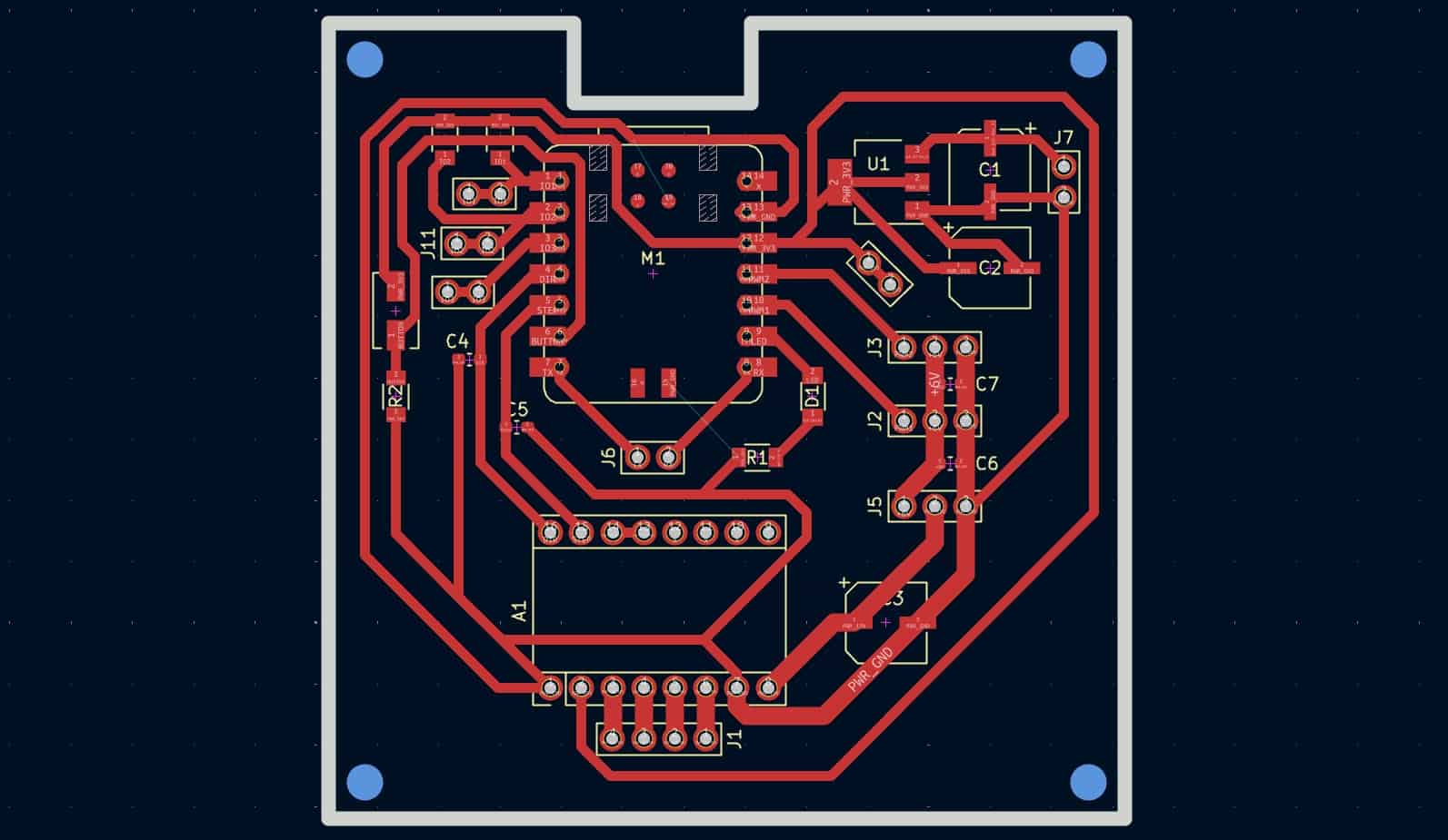
V3's layout is based on V2's, with the main difference being the placement I/O pins, where I had to re-arrange the dual pin headers to accommodate the traces connected to the pull-up resistors.
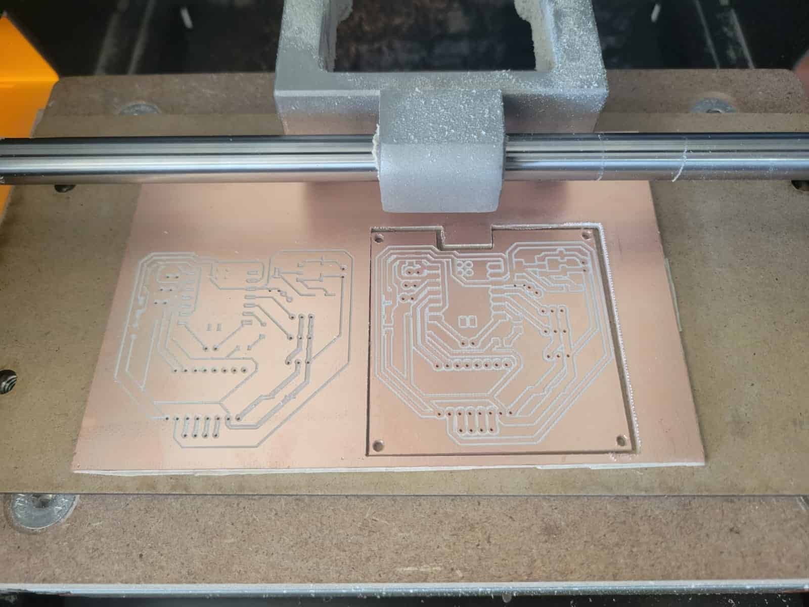
The fabrication of the board was the same as in previous weeks, starting by plotting the SVGs of the F.Cu, Edge.Cuts, User.1 and User.2 layers. I processed these SVGs into toolpaths for the monoFab using the mods.ce webpage as usual.
I followed the usual procedure in the monoFab, setting the fixed X/Y origin and establishing the Z origin each time I changed tools. I started by drilling the holes drawn in the User.1 layer with a 0.8mm flat endmill, then the traces of the F.Cu layer using the 10° V-bit cutter. Unfortunately, I made some changes to the design and processed the toolpath without inverting the colors. Which resulted in an inverted carving, but this is no serious problem, with plenty of board to spare, I simply re-established the X/0 and started from the beginning.
Since the board had a slight inclination, some traces weren't carved out on the first pass. Having learned from previous experience, I decided to take the slow and steady path and did two whole passes, the second being 0.1mm deeper than the first. This proved to be succesful, and the results were by far the cleanest traces that I have done until now.
I then cut the holes in the corners, drawn in the User.2 layer, and finally, the Edge.Cuts layer, both processes were done with the 1.2mm flat endmill.
After being done with the monoFab, I soldered my components, as usual, starting from the center and going outwards.
This is how V3 came out, the best one far;
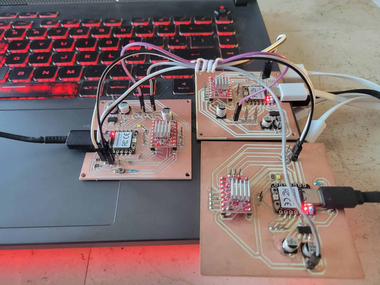
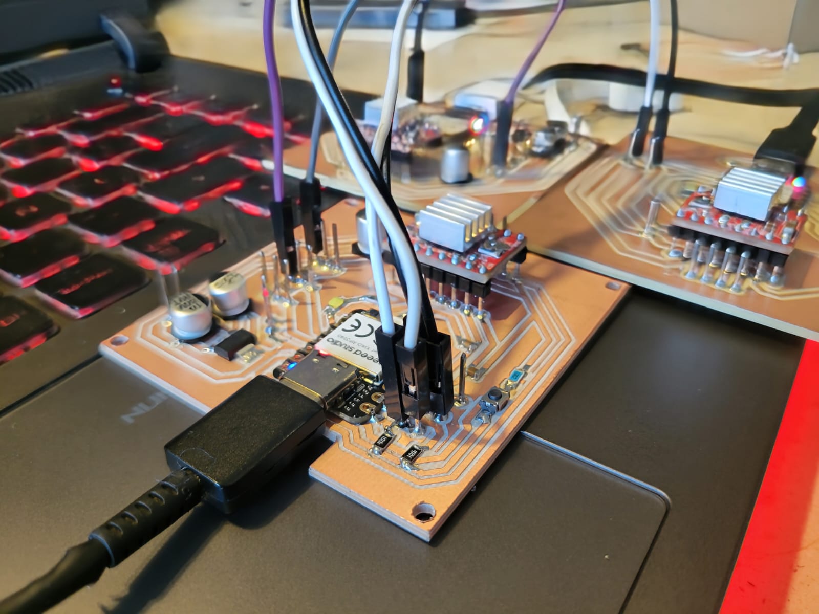
With all my PCBs ready, I connected the dual pin headers connected to the D0 and D1 pins of V3 to the D0 and D1 pins on V1 and V2 with DuPont cables, these will be my SDA and SCL lines respectively.
Finally, I connected the grounds on all three devices and connected them to my PC through the Type-C port, completing the physical setup.
4.2 Programming
The programming phase of this assignment focused on establishing a simple and reliable I2C communication protocol, with V1 being the main board and V1 and V2 acting as the two secondary boards. As previously mentioned, communication was facilitated through the D0 (SDA) and D1 (SCL) pins, with 4.7 kΩ pull-up resistors integrated into V1 for stable signal levels.
4.2.1 Main Board CodeOur main board, V3, acts as the I2C controller (previously referred to as "master"), orchestrating communication with the two secondary nodes. It listens for user input via the serial monitor and a button connected to pin D5. We will write a command on the serial monitor to specify which of the secondary boards we wish to communicate with, after which, each time the button is pressed, the main board sends a specific command to the selected secondary board, instructing it to activate its LED for one second.
#include <Wire.h>

#define SDA_PIN D0
#define SCL_PIN D1
#define BUTTON_PIN D5

int selectedAddress = 0x01;  //S1 Default
bool lastButtonState = LOW;

void setup() {
    pinMode(BUTTON_PIN, INPUT);
    Wire.setSDA(SDA_PIN);
    Wire.setSCL(SCL_PIN);
    Wire.begin();
    Serial.begin(115200);
    Serial.println("Type '1' for secondary 1 or '2' for secondary 2.");
}

void loop() {
    if (Serial.available()) {
        char input = Serial.read();
        if (input == '1') {
            selectedAddress = 0x01;
            Serial.println("Selected Secondary 1 (0x01)");
        } else if (input == '2') {
            selectedAddress = 0x02;
            Serial.println("Selected Secondary 2 (0x02)");
        }
    }

    bool buttonState = digitalRead(BUTTON_PIN);
    if (buttonState == HIGH && lastButtonState == LOW) {
        Wire.beginTransmission(selectedAddress);
        Wire.write(1);
        Wire.endTransmission();
        Serial.print("Signal sent to address 0x");
        Serial.println(selectedAddress, HEX);
        delay(200);
    }
    lastButtonState = buttonState;
}
1. We begin by including the Wire library, which provides the functionality needed for I2C communication and simplifies handling main-secondary communication protocols. We then define the specific GPIO pins used in our setup with identifiable labels.
#include <Wire.h>

#define SDA_PIN D0
#define SCL_PIN D1
#define BUTTON_PIN D5
2. We define two global variables:
int selectedAddress = 0x01;  //S1 Default
bool lastButtonState = LOW;
int selectedAddress = 0x01;holds the I²C address of the currently selected secondary device. By default, it's set to 0x01, which corresponds to Secondary 1.bool lastButtonState = LOW;helps in detecting a button press event by storing the previous state of the button.
3. The
setup() function runs once when the board powers on:
void setup() {
    pinMode(BUTTON_PIN, INPUT);
    Wire.setSDA(SDA_PIN);
    Wire.setSCL(SCL_PIN);
    Wire.begin();
    Serial.begin(115200);
    Serial.println("Type '1' for secondary 1 or '2' for secondary 2.");
}
pinMode(BUTTON_PIN, INPUT);sets the button pin as an input. Since we're using an external pull-down resistor, this pin reads LOW by default and switches to HIGH when pressed.Wire.setSDA()andWire.setSCL()explicitly assign the I²C lines to the appropriate GPIO pins.Wire.begin()initializes I2C communication as a master.Serial.begin(115200);initializes serial communication at 115200 baud, allowing us to interact with the microcontroller via the serial monitor.- The printed message invites the user to choose a secondary board for communication.
4. This section continuously checks if the user has typed something into the serial monitor. If '1' or '2' is received, the
selectedAddress variable is updated accordingly. This mechanism lets us choose which secondary device we want to control.
void loop() {
    if (Serial.available()) {
        char input = Serial.read();
        if (input == '1') {
            selectedAddress = 0x01;
            Serial.println("Selected Secondary 1 (0x01)");
        } else if (input == '2') {
            selectedAddress = 0x02;
            Serial.println("Selected Secondary 2 (0x02)");
        }
    }
5. Our last section implements the logic for the button press:
bool buttonState = digitalRead(BUTTON_PIN);
    if (buttonState == HIGH && lastButtonState == LOW) {
        Wire.beginTransmission(selectedAddress);
        Wire.write(1);
        Wire.endTransmission();
        Serial.print("Signal sent to address 0x");
        Serial.println(selectedAddress, HEX);
        delay(200);
    }
    lastButtonState = buttonState;
}
digitalRead(BUTTON_PIN)captures the current state of the button.- The conditional
if (buttonState == HIGH && lastButtonState == LOW)detects the moment the button is pressed. - Upon detecting a press, the board sends a single byte (1) to the selected secondary using:
Wire.beginTransmission(selectedAddress);Wire.write(1);Wire.endTransmission();
- A confirmation is printed via the serial monitor.
delay(200);prevents accidental bouncing and allows time between commands.- Finally, we update
lastButtonStateto track button state history.
The code programmed into the V1 and V2 enables the microcontroller to act as an I²C secondary device, listening for signals sent from the main board. Each secondary has a unique address, allowing the main board to target them individually. When the message is received, the board briefly turns on its LED for one second.
#include <Wire.h>

#define SDA_PIN D0
#define SCL_PIN D1
#define LED_PIN D8 // D5 for Secondary 2

#define MY_ADDRESS 0x01  // 0x02 for Secondary 2

void receiveEvent(int howMany);

void setup() {
    pinMode(LED_PIN, OUTPUT);
    Wire.setSDA(SDA_PIN);
    Wire.setSCL(SCL_PIN);
    Wire.begin(MY_ADDRESS);
    Wire.onReceive(receiveEvent);
    Serial.begin(115200);
    Serial.print("Secondary at 0x");
    Serial.print(MY_ADDRESS, HEX);
    Serial.println(" ready.");
}

void loop() {
}

void receiveEvent(int howMany) {
    while (Wire.available()) {
        int cmd = Wire.read();
        if (cmd == 1) {
            digitalWrite(LED_PIN, HIGH);
            delay(1000);
            digitalWrite(LED_PIN, LOW);
        }
    }
}
1. As with the main board, we begin by including the Wire library, which allows this microcontroller to act as an I²C secondary device. We define the pins and the unique adress of the device. I placed comments in the code to indicate that the LED pin and the adress are different in V1 from the ones in V2, other than this the code is the same in both devices.
#include <Wire.h>

#define SDA_PIN D0
#define SCL_PIN D1
#define LED_PIN D8 // D5 for Secondary 2

#define MY_ADDRESS 0x01  // 0x02 for Secondary 2
2. This line declares the function
receiveEvent, which will later be registered as the callback to run when data arrives from the main board. This is how secondaries listen for incoming I2C messages.
void receiveEvent(int howMany);
3. We establish the setup:
void setup() {
    pinMode(LED_PIN, OUTPUT);
    Wire.setSDA(SDA_PIN);
    Wire.setSCL(SCL_PIN);
    Wire.begin(MY_ADDRESS);
    Wire.onReceive(receiveEvent);
    Serial.begin(115200);
    Serial.print("Secondary at 0x");
    Serial.print(MY_ADDRESS, HEX);
    Serial.println(" ready.");
}
- The LED pin is set as an output.
- The I2C lines are configured to match the physical connections.
Wire.begin(MY_ADDRESS);initializes the device as a secondary with its unique address.Wire.onReceive(receiveEvent);links incoming data to our handler function.- We establish serial communications, printing a message to confirm the address of the secondary on startup.
4. The
loop() function is intentionally left empty. The board is not actively checking for input; instead, it reacts to I2C commands via an interrupt based system.
void loop() {
}
5. Finally, we establish the core of the secondary board's behavior as a secondary device.
void receiveEvent(int howMany) {
    while (Wire.available()) {
        int cmd = Wire.read();
        if (cmd == 1) {
            digitalWrite(LED_PIN, HIGH);
            delay(1000);
            digitalWrite(LED_PIN, LOW);
        }
    }
}
- When data is received from the main board, this function is automatically called.
Wire.available()checks for bytes in the receive buffer.Wire.read()fetches the incoming data, in our case, a single byte (1) is expected.- If that command equals "1", the LED is turned on for 1 second and then turned off.
5. Results
With our system ready, I conducted the test.
The system worked succesfully, allowing us to select the specific secondary device that we want to communicate with, and sending the command to turn its LED on whenever the button on the main device is pressed.
For this week's hero shot, I chose this picture of the setup;
6. Comments and Recommendations
This was my first time working with synchronous serial communication protocol, having only used UART before. I like the new possibilities that come with these protocols, giving me more tools to develop bigger and better communicated systems.
The coding process had it's difficulties, since I had little knowledge on the syntax used in I²C, but by researching and starting with simple codes, it turned out more straight-forward than anticipated.
I have grown quite fond of the XIAO microcontroller unit, it's small size and versatility makes it an incredible resource for small projects. I have yet to try XIAOs other than the RP2040, but I certainly look forward to it in the near future.
7. Learning Outcomes
This week I designed and manufactured my V3 PCB, my best one so far, and very likely to be the one I use for my final project. I used this device in conjunction with my previous V1 and V2 PCBs to create a communicated system using the I²C protocol.
I look forward to new communicated projects in the future, and diving deeper into both wired and wireless communications.