Week 6
Electronics Design
Summary of Activities
This week focused on electronics design. The individual assignment involved creating and checking a custom development board using components from the Fab Lab inventory. The objective was to integrate microcontroller interaction and communication capabilities. As a group, we were also required to explore and test microcontroller boards using lab equipment such as oscilloscopes and multimeters.
Assignment Requirements
- ✅ Use EDA software to design and verify a development board
- ✅ Include interaction and communication capabilities with a microcontroller
- ✅ Extra credit: test a different workflow
- ✅ Extra credit: simulate the circuit
- ✅ Extra credit: design a case for the board
Group Assignment - Week 4
The objective is to demonstrate and compare the toolchains and development workflows for available embedded architectures. This involves hands-on testing and documentation of programming environments used across different microcontrollers.
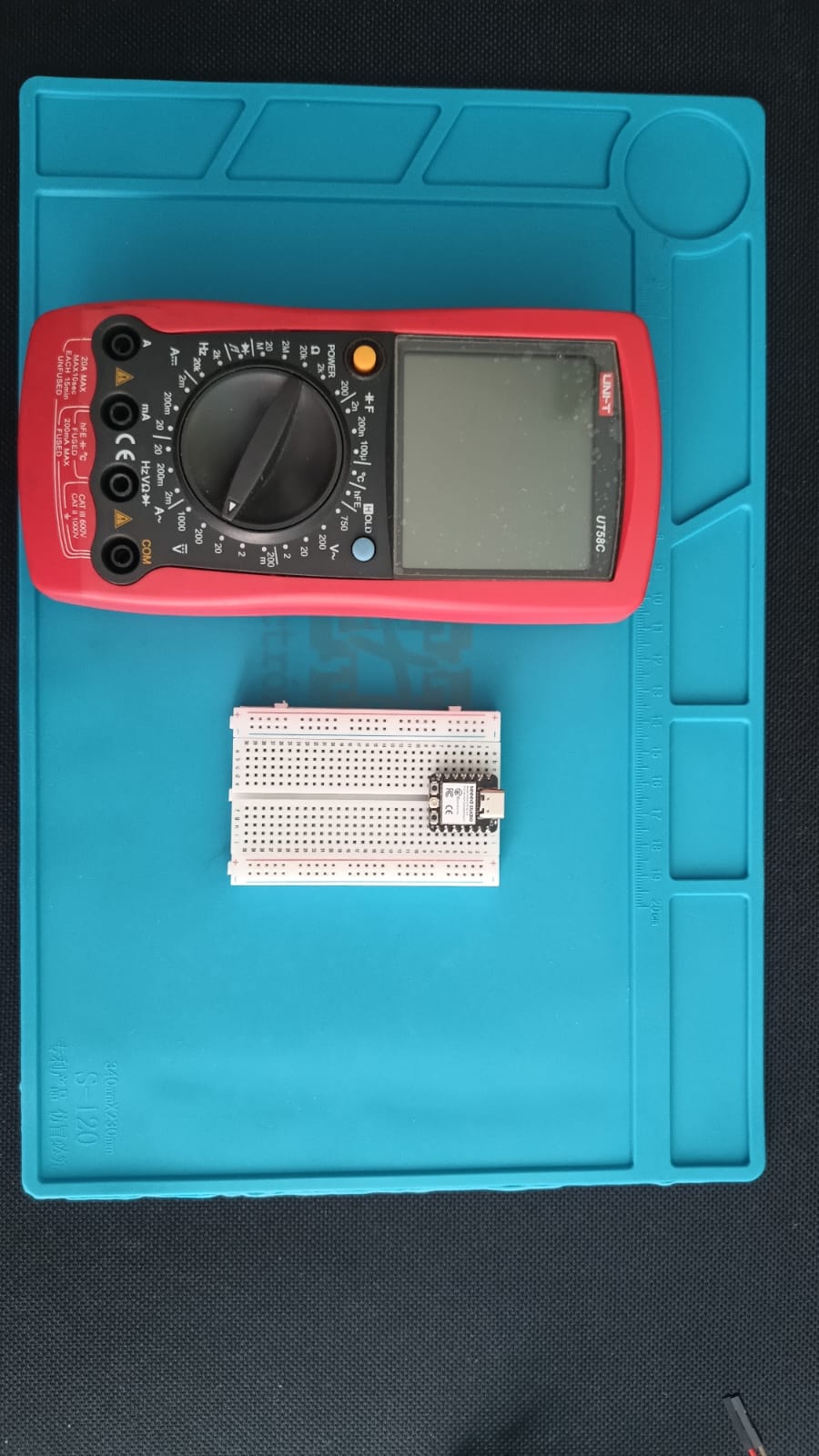
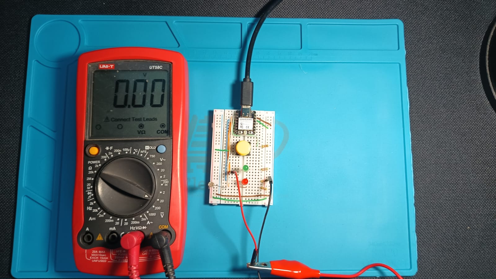
To verify the use of a development board with laboratory equipment, I prepared my XIAO ESP32 C3 board, a multimeter, and an oscilloscope on a clean work surface.
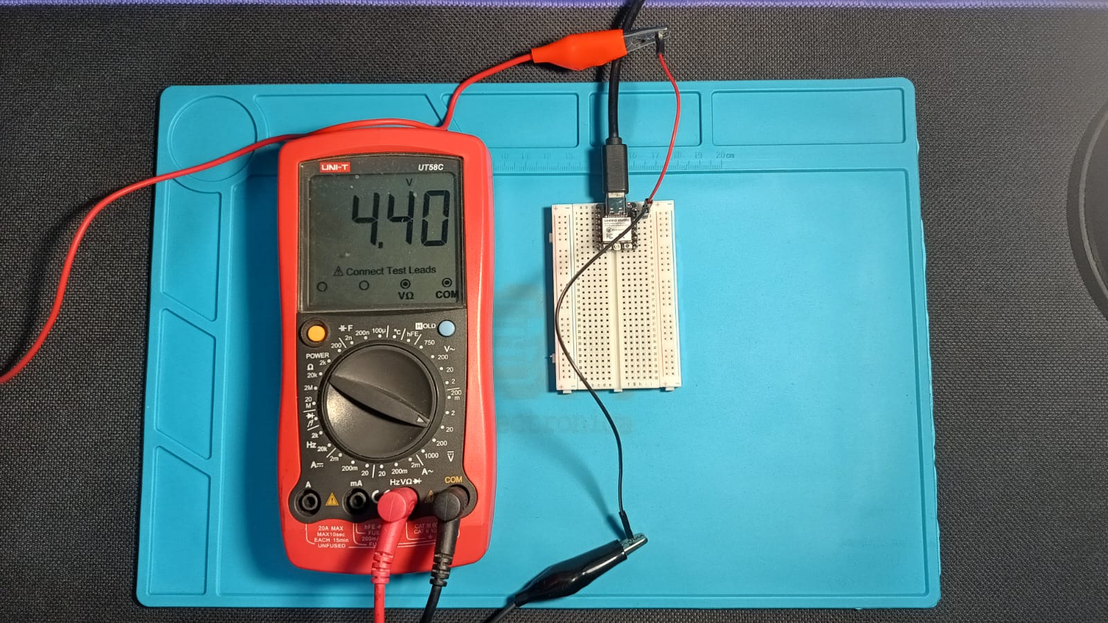
I then measured the voltage output from the 5V pin of the microcontroller and obtained a reading of 4.4 volts, which is the unit used to measure electric potential. This is significant because, although the datasheet indicates a 5V output, there are acceptable tolerance levels, and in real systems, internal losses and resistive elements cause small drops that theoretical models do not usually account for.
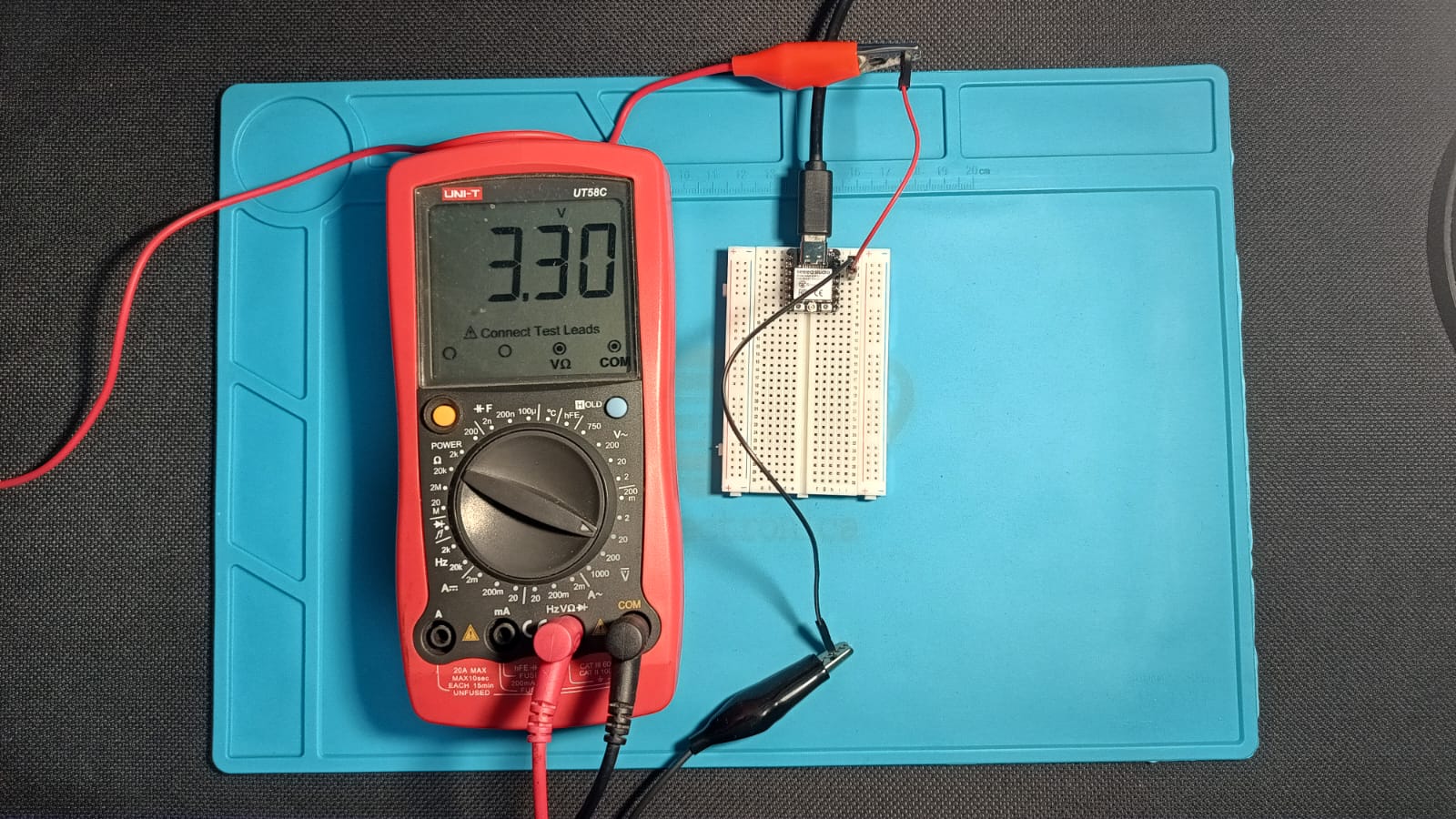
I also measured the voltage at the 3.3V output. It is important to note that electric potential must be measured relative to ground (GND), and the multimeter should be set to the voltage section marked with a solid line, indicating it is measuring DC voltage. This type of voltage is present in DC power sources, batteries, and other systems that generate direct current.
Since my test setup initially used long jumper wires and appeared disorganized, I decided to improve it by using UTP cable to make the connections as close to the breadboard as possible. This made it easier to quickly take measurements and identify any faults in the circuit.
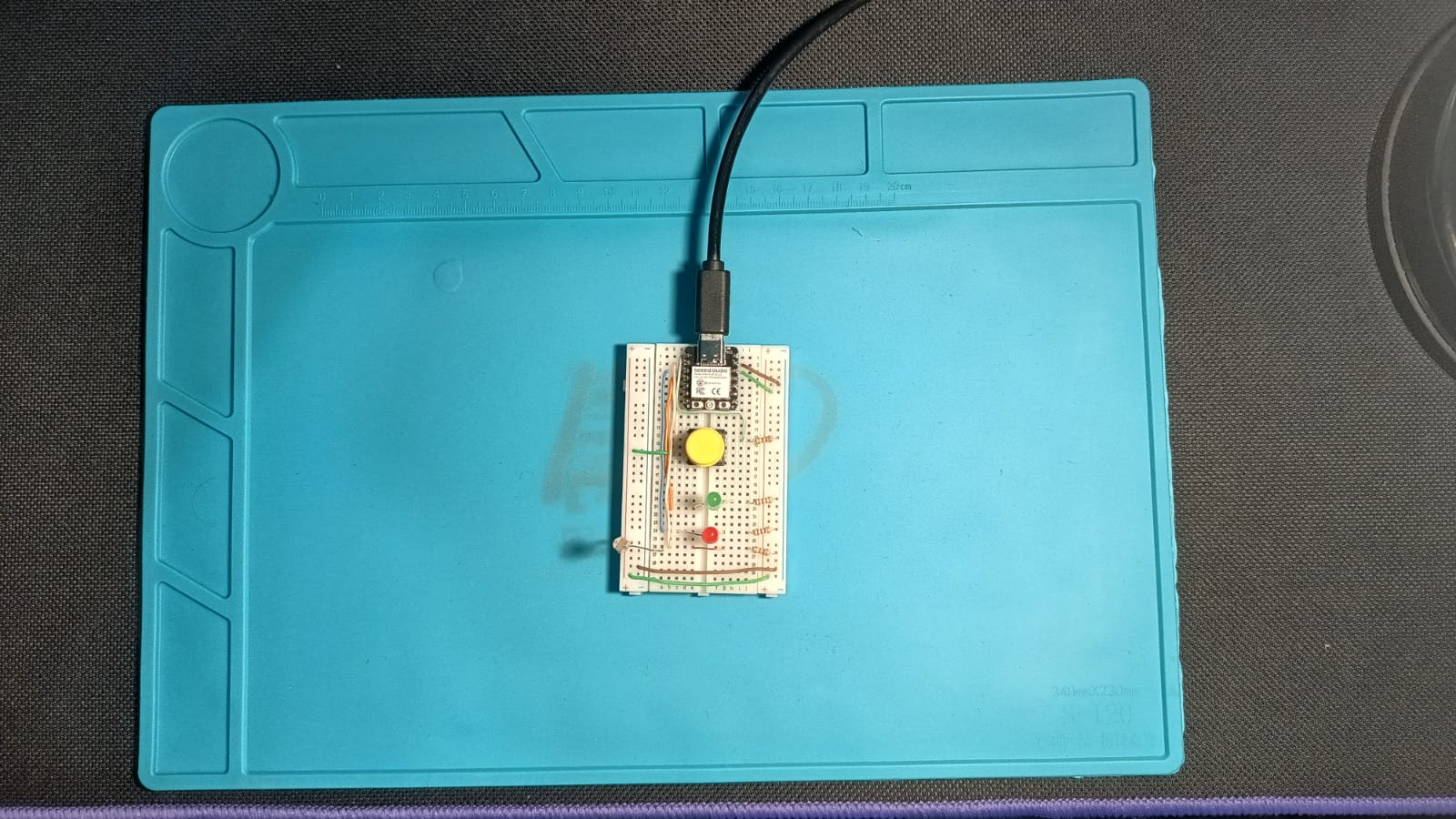
Measuring Voltage on the Green LED
To measure the output voltage on the green LED, I added extra wires with jumpers to make the process easier. This LED is only activated when the light detected by the photoresistor drops significantly.
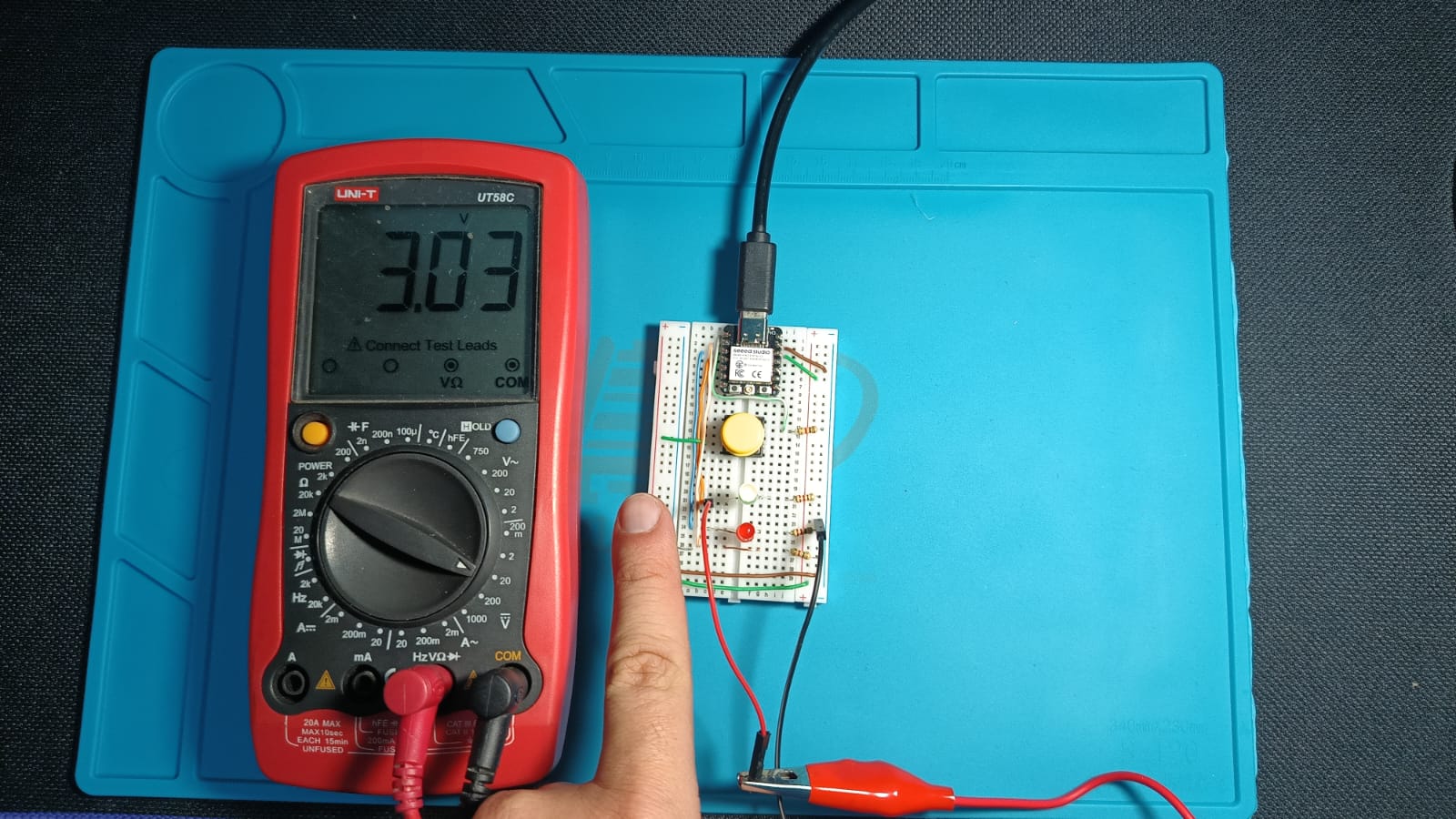
LED On and Multimeter Reading
Once the light on the photoresistor was reduced, the green LED turned on and the multimeter registered a voltage of approximately 3.03 V.
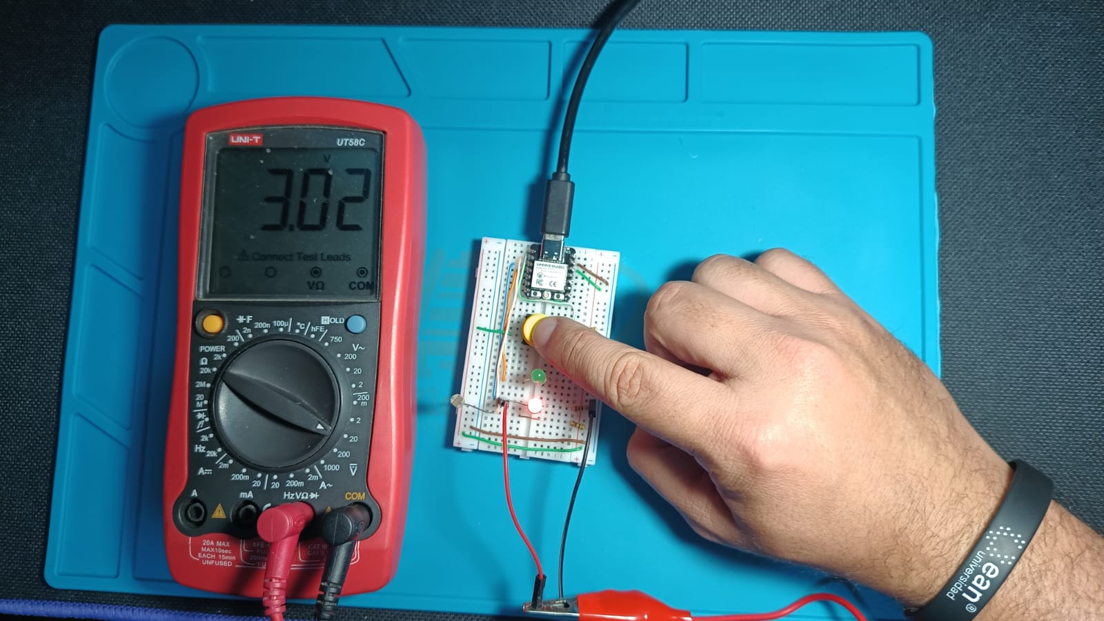
Button Press and Red LED Voltage
Now, by pressing the yellow button, the red LED should light up. I had previously changed the probe connections to measure the input voltage to the red LED, obtaining a reading of approximately 3.02 V.
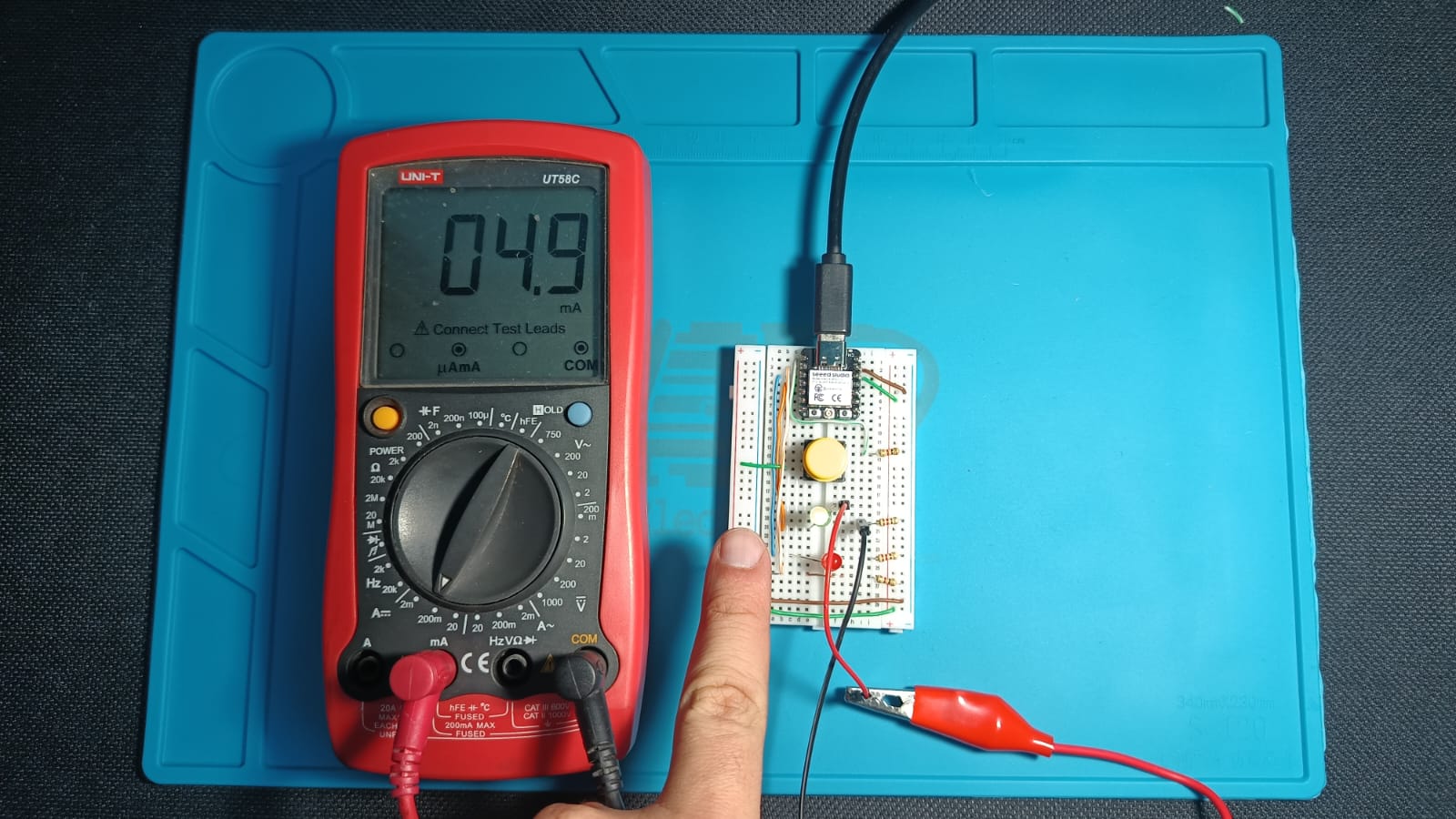
Measuring Current with Ammeter
After switching the multimeter to its ammeter function, I obtained a current reading of 4.9 mA.
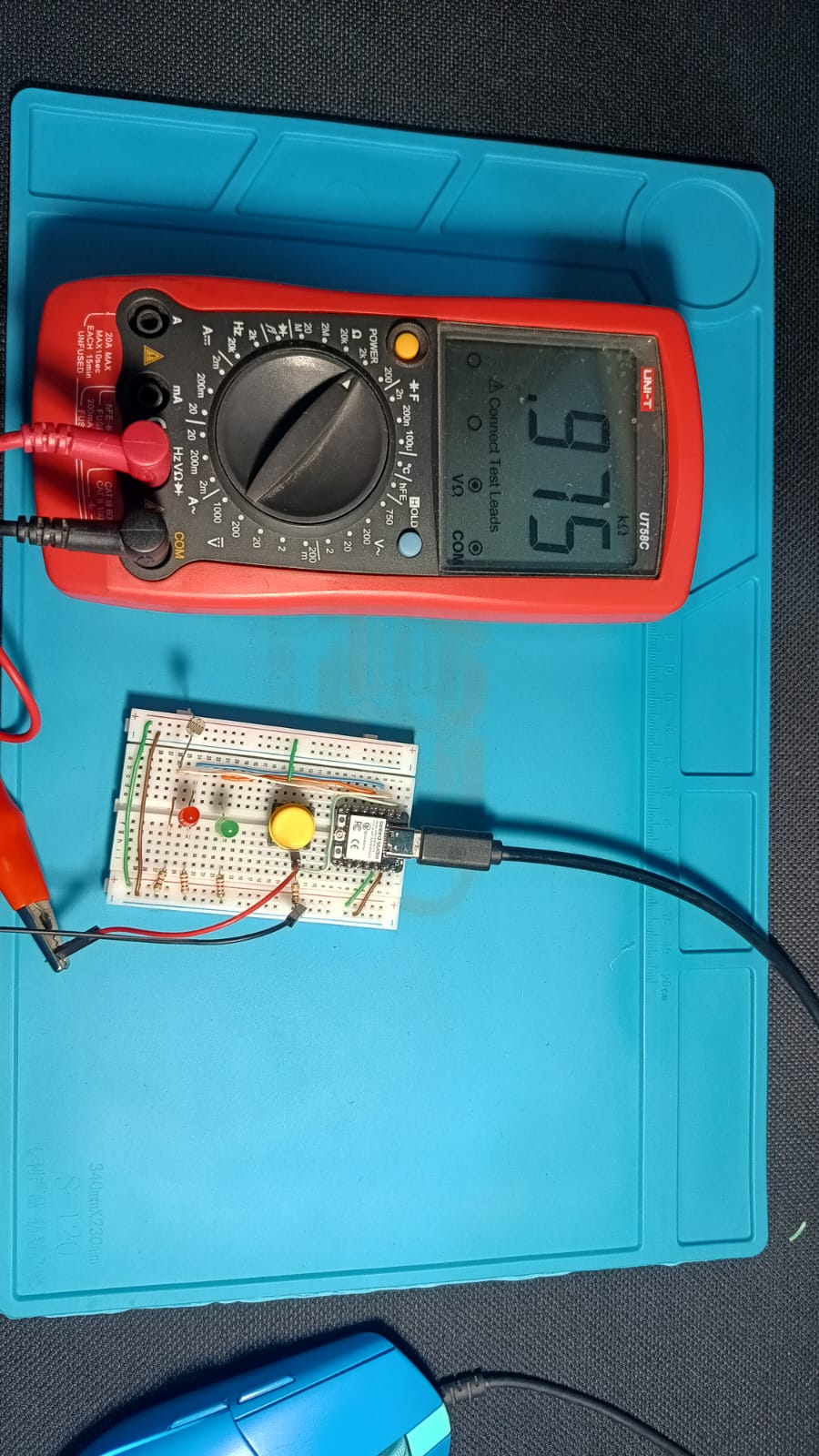
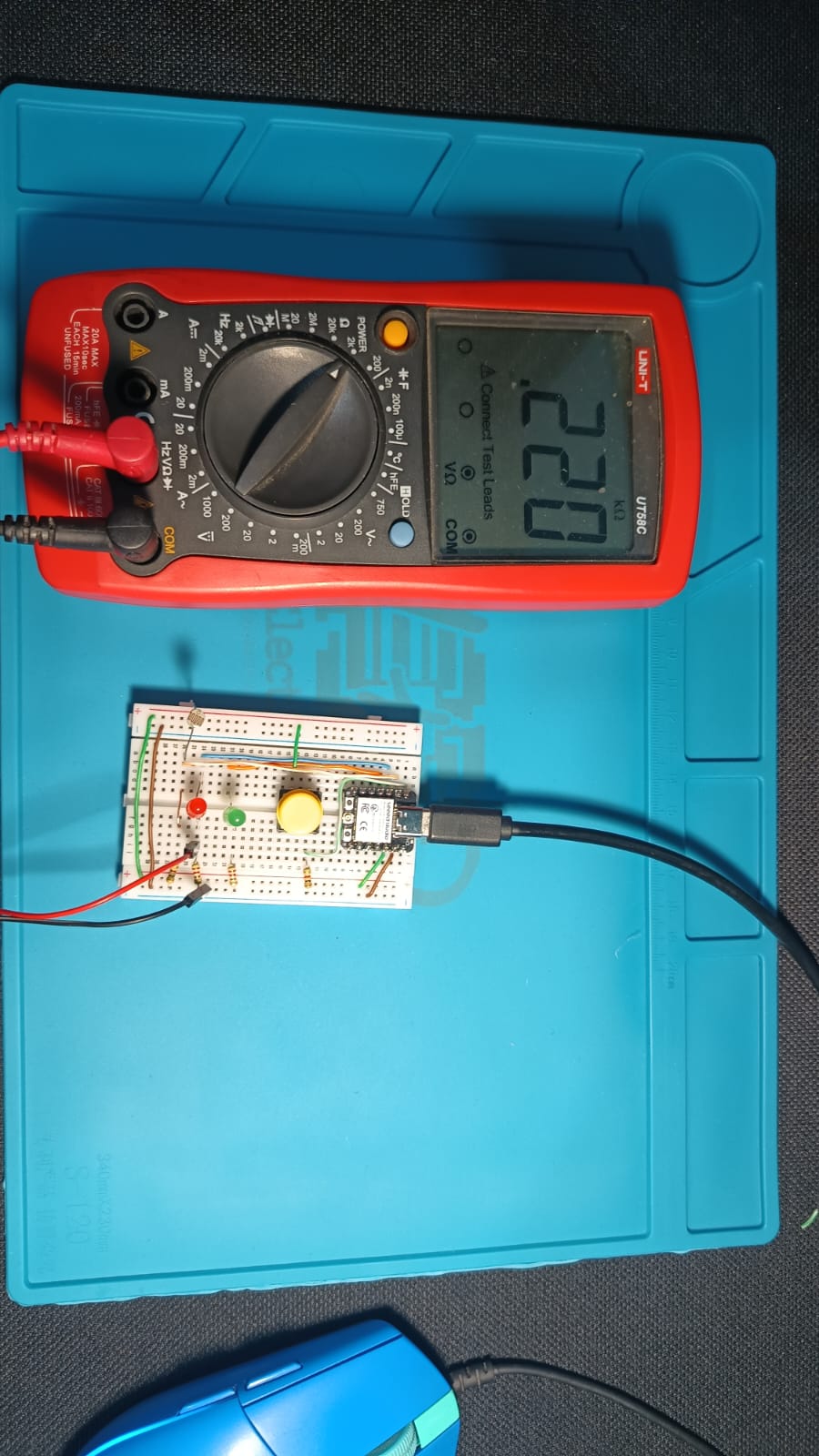
Verifying Resistor Values
I then verified the values of the 220-ohm and 1-kilo-ohm resistors, obtaining measurements very close to their nominal ratings. The small differences observed are due to the tolerance specified by manufacturers during the production of these components.
Oscilloscope Measurements
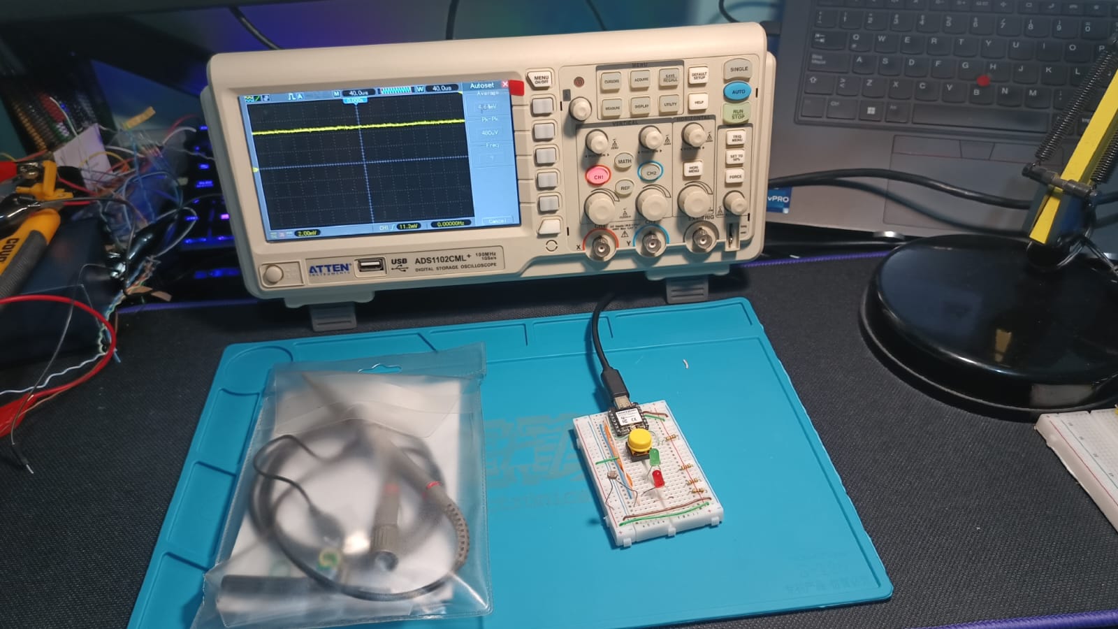
To complement the electrical characterization of the microcontroller circuit, I used an oscilloscope to visualize voltage waveforms at different points of the system. This allowed me to observe signal stability, transitions, and behavior under different conditions. Oscilloscopes are essential for analyzing real-time variations in voltage, making them ideal for validating digital states, pulse widths, and analog sensor responses.
I now used an oscilloscope to visualize the waveform signals present in the circuit. To do this, it is necessary to use probes that have an attenuation factor, typically x1 or x10. Depending on the signal type and amplitude, one or the other is selected for optimal measurement and display.
In the following video, it can be observed how reducing the light over the photoresistor significantly increases the waveform signal at the green LED input. When the ambient light returns to its normal intensity, the signal drops back to approximately 0 V.
In the following video, the waveform can be observed in greater detail, clearly showing the voltage increase when the light intensity over the photoresistor is reduced, and its return to approximately 0 V when normal lighting conditions are restored.
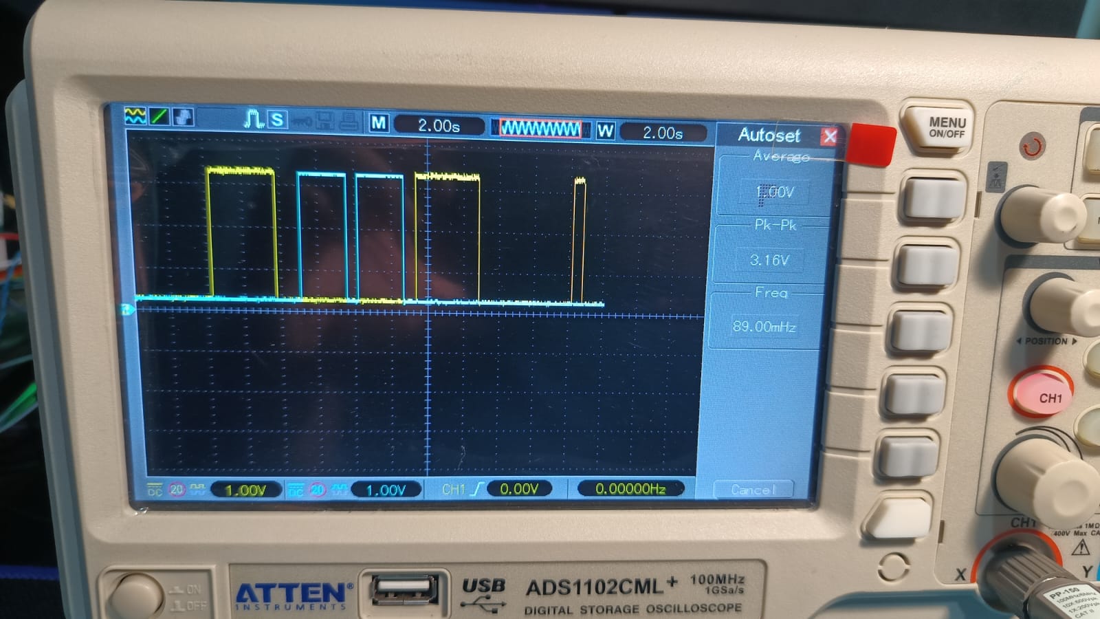
To simultaneously observe both signals, I connected both oscilloscope probes—each to the input of a different LED. As shown in the video, each waveform increases when its corresponding LED is activated.
Finally, the following image shows in detail the waveform captured by the oscilloscope. One important value to highlight is the 1 V label located at the lower left corner of the screen—this indicates that each vertical division on the oscilloscope corresponds to 1 volt. Based on this scale, it can be observed that each signal reaches approximately 3.1 V. Since it is not a periodic signal (which repeats at regular time intervals), the oscilloscope displays a frequency of 0 Hz.
Reflections on the Measurement Process
- Performing voltage and current measurements using a multimeter helped to understand the real behavior of electrical components under working conditions. It became evident that theoretical values may vary slightly due to factors such as resistance tolerances and energy losses in the system.
- The process of optimizing the wiring by replacing long and disorganized jumper cables with UTP cables improved not only the clarity of the setup but also the precision in identifying faults or making measurements.
- Observing waveforms with the oscilloscope allowed a deeper analysis of the circuit’s dynamic behavior. It provided clear visual confirmation of how analog and digital signals respond to changes in input, such as light intensity or the press of a button.
- The use of the oscilloscope highlighted the importance of understanding how signal amplitude and frequency relate to real-world interactions. Measuring a frequency of 0 Hz reinforced the concept that not all signals are periodic, especially in user-interactive systems.
- Overall, integrating theoretical knowledge with hands-on instrumentation reinforced the importance of accurate measurement and documentation when working with embedded systems.
EDA Design with KiCad
This section documents the individual work for week 6, focused on designing a custom development board using an EDA tool and a microcontroller from the Fab Academy inventory.
1. Microcontroller Selection
The microcontroller selected for this assignment is the RP2040, developed by Raspberry Pi. It is a powerful and cost-effective dual-core ARM Cortex-M0+ MCU that balances performance, efficiency, and accessibility—ideal for custom development boards in digital fabrication environments.
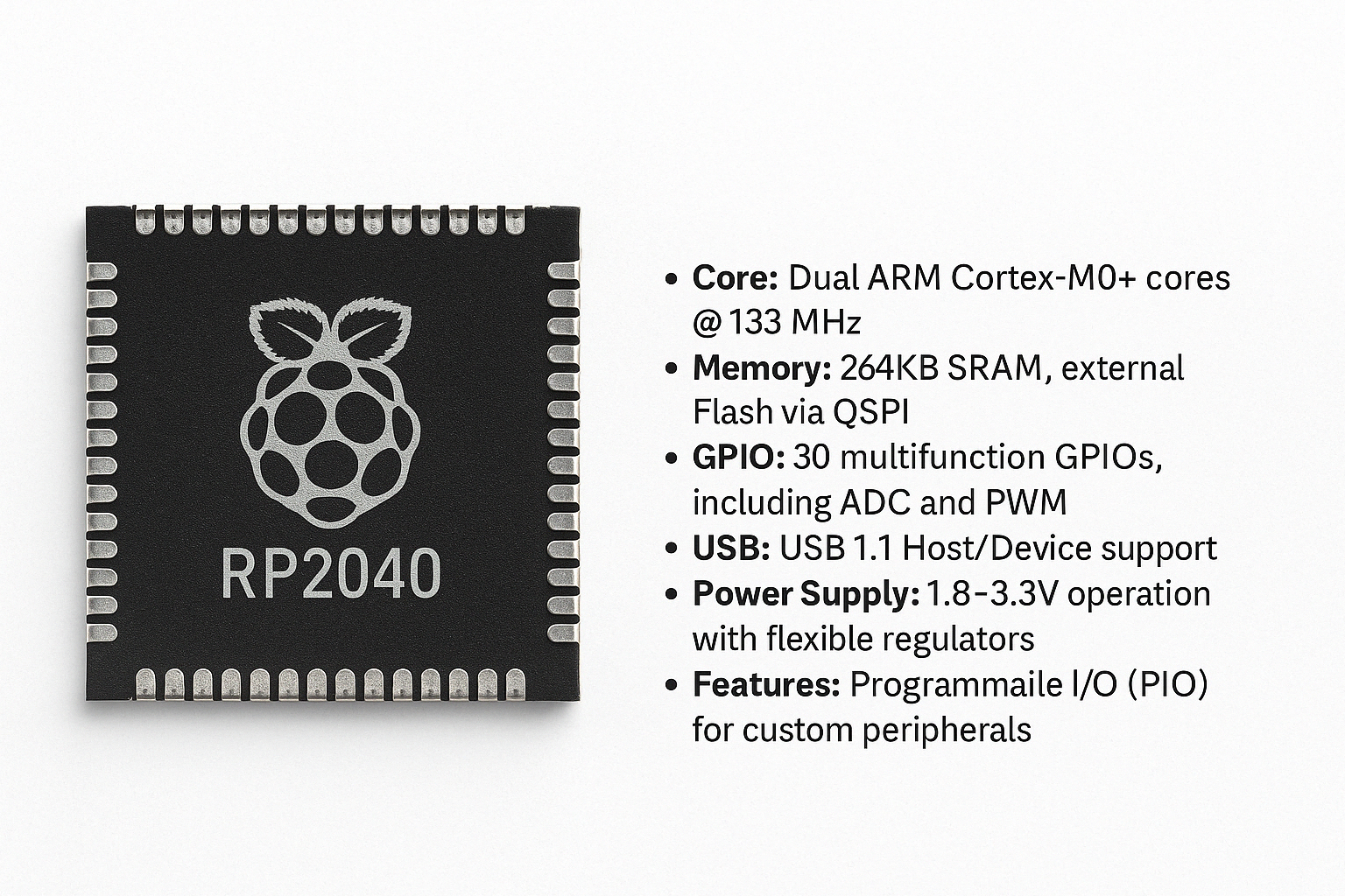
This microcontroller is widely adopted in educational and maker environments due to its simplicity and powerful peripherals. It supports C/C++, MicroPython, and CircuitPython, making it extremely versatile. The RP2040 also integrates easily into PCB design workflows using KiCad or other EDA tools, and its availability within the Fab inventory makes it a natural choice for this development task.
2. Project Setup in KiCad
For this assignment, Professor Ulises organized a dedicated session to explain and guide us through the KiCad design process. Several classmates attended the session, where we had the opportunity to ask questions and explore the EDA workflow in a collaborative environment.
In the following sequence, I document the process of configuring KiCad to work with custom FabAcademy libraries, including downloading, organizing folders, and linking symbol and footprint paths. This ensures a smoother design workflow tailored to the inventory components provided for the assignment.
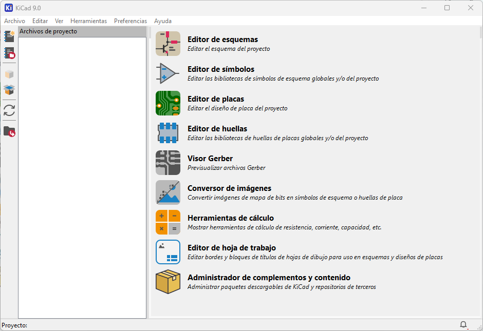
Step 1: Opening KiCad and Starting a New Project
I opened KiCad and selected the option to create a new project. This initializes a workspace where both the schematic and PCB layout can be developed.
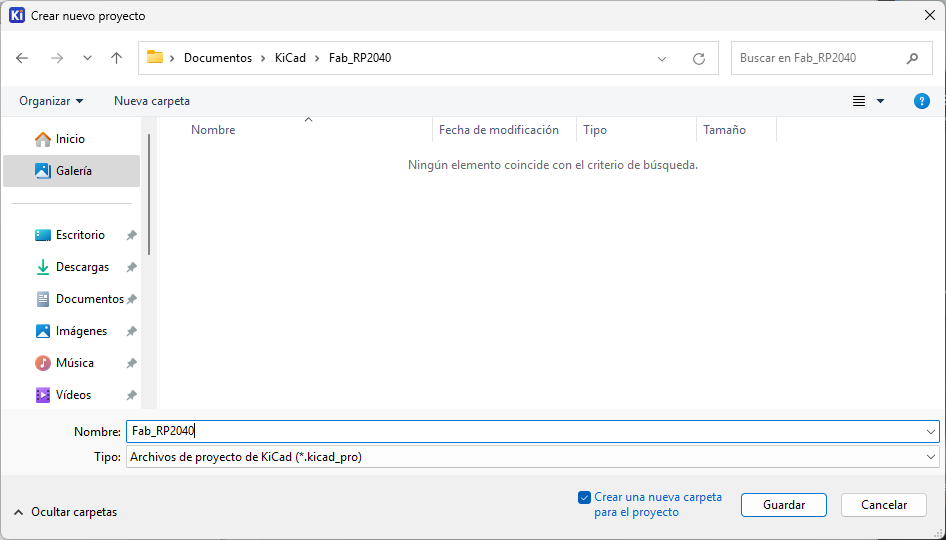
Step 2: Creating a Folder for the Project
I created a folder named Fab_RP2040 inside the default KiCad repository to organize and store all the project files, ensuring a clean and structured workflow.
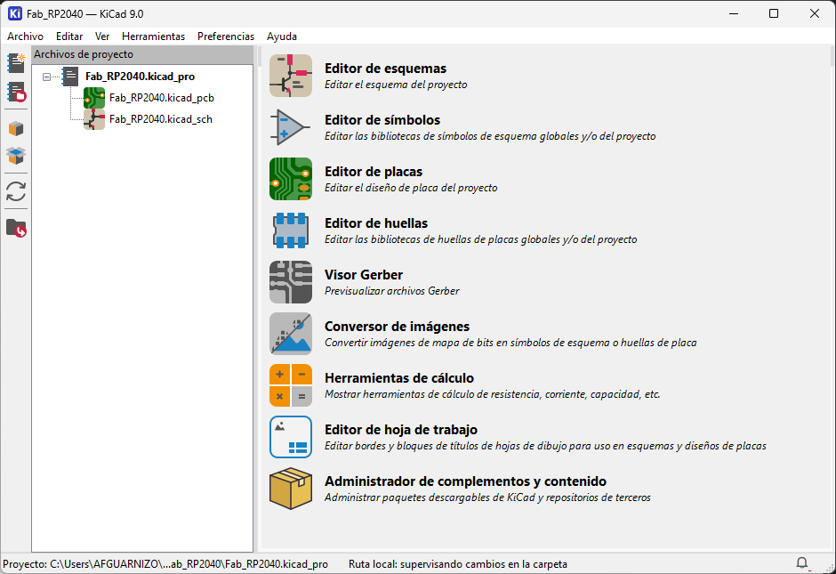
Step 3: Project Files Created
Two files were automatically created by KiCad: one for the schematic design and another for the PCB layout. This structure keeps the workflow organized and allows for a smooth transition between design and routing stages.
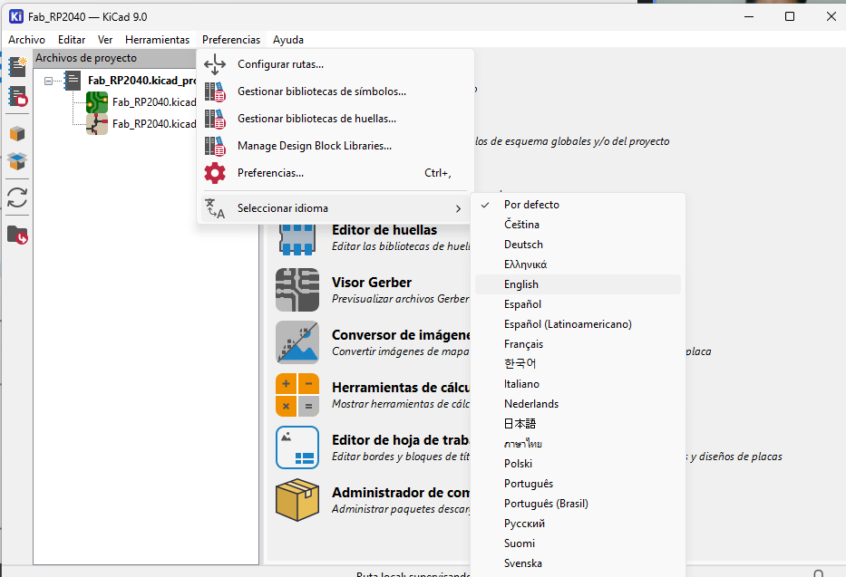
Step 4: Switching the Interface Language
At this point, I realized that the software interface was in Spanish. To maintain consistency with the documentation and tutorials, I switched the language settings to English from the preferences menu.
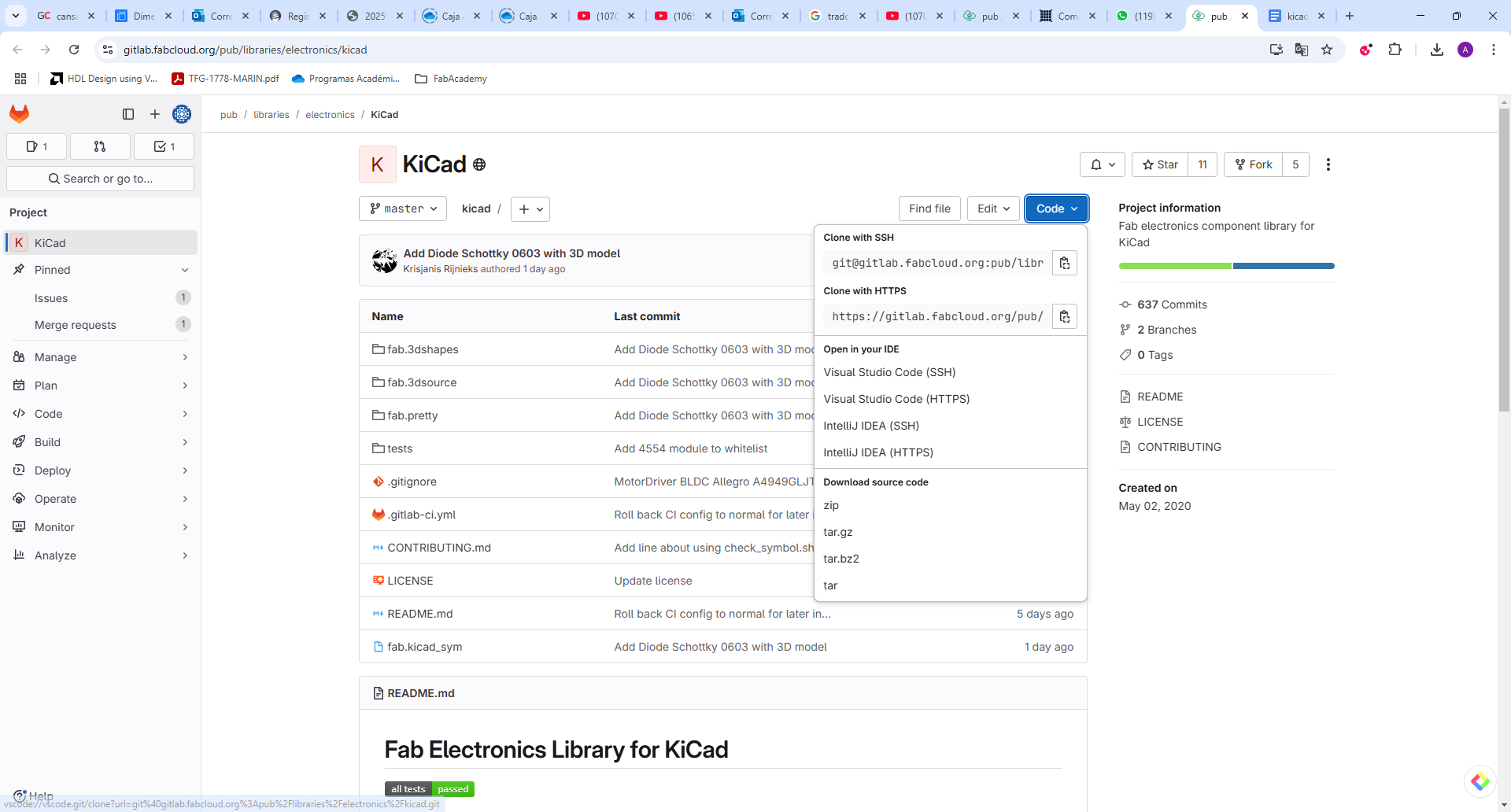
Step 5: Downloading the Fab Library
Following the advice of Professor Ulises, I downloaded a library that includes the most commonly used footprints, 3D models, and symbols in the Fab Academy. This resource will make the design process much easier as it ensures compatibility with our fabrication workflow.
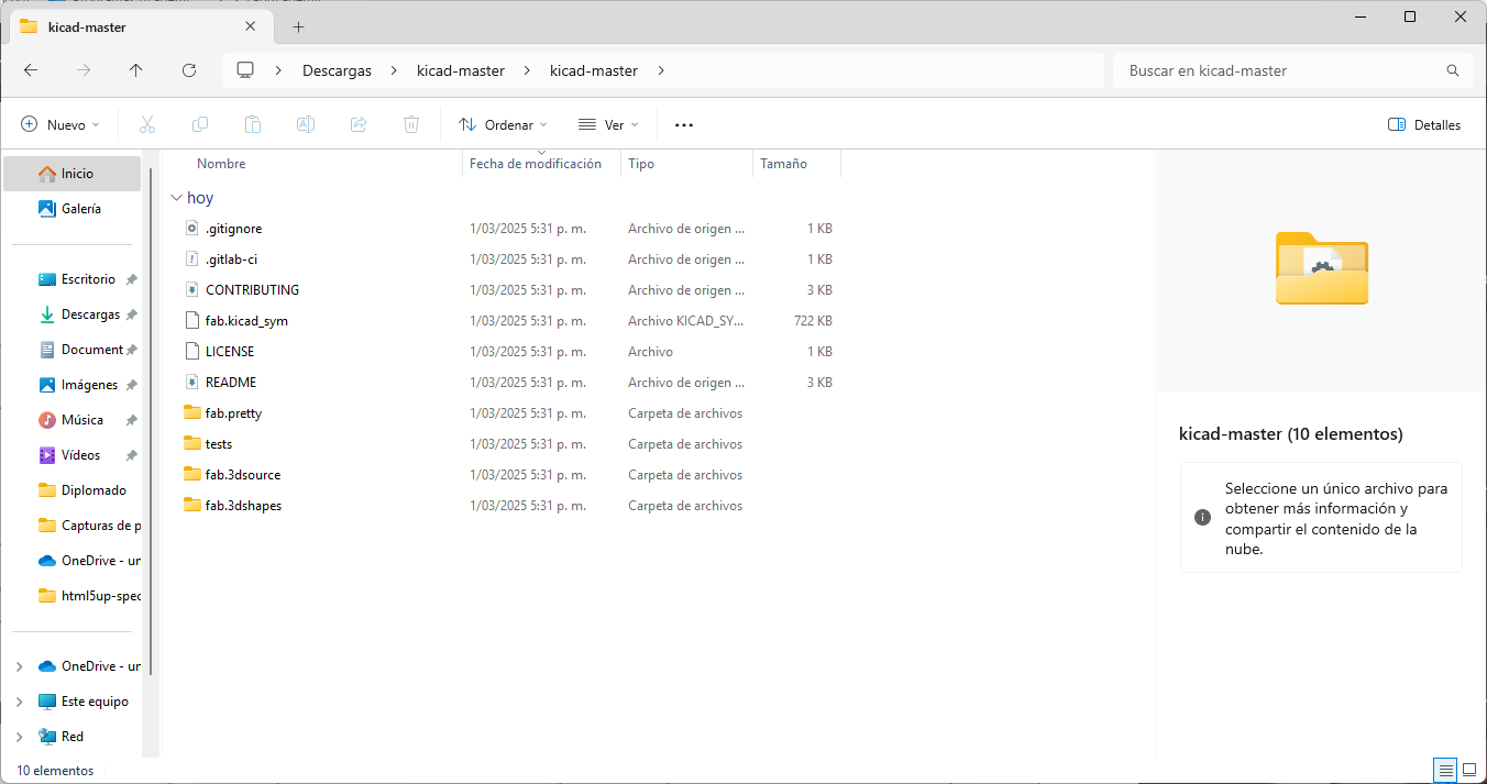
Step 6: Library Contents
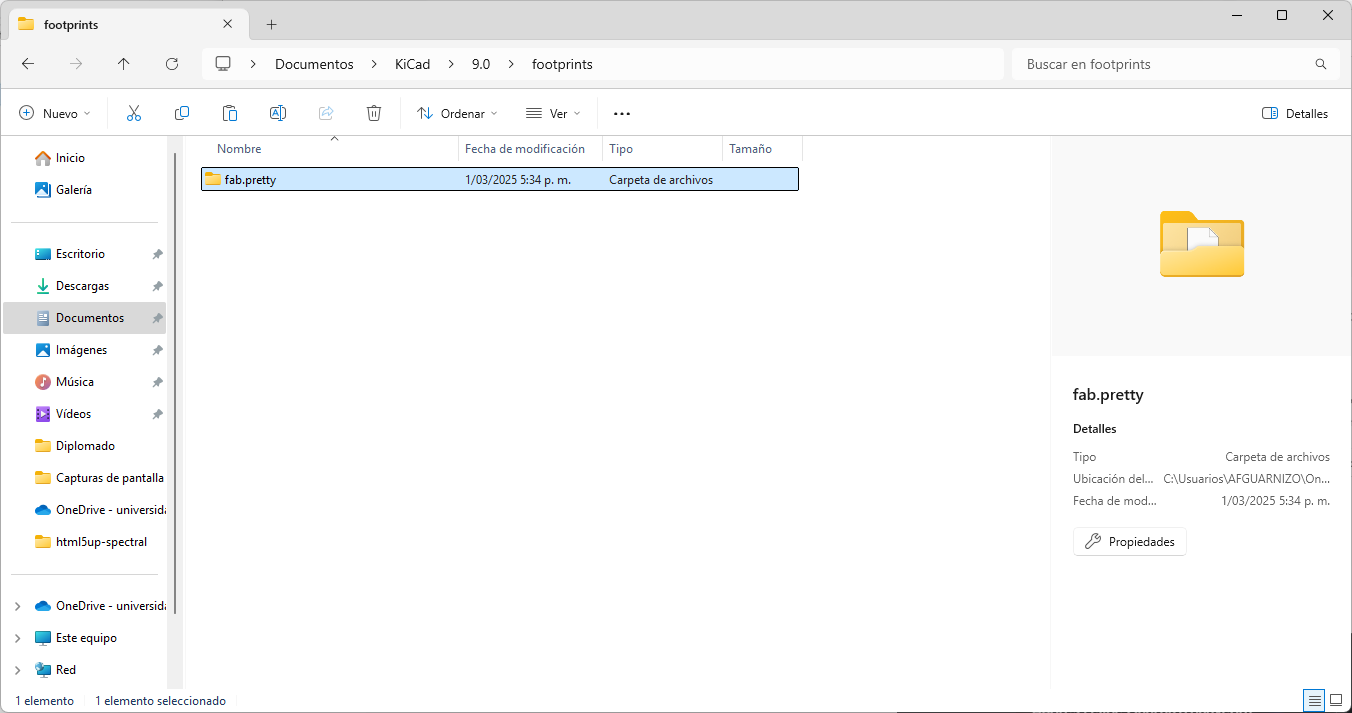
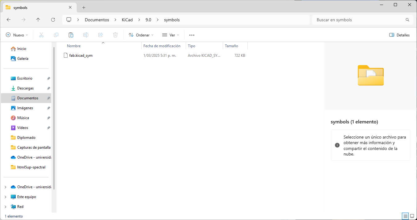
Here you can see the contents of the library after it was downloaded and unzipped in the Downloads folder. It includes multiple folders for symbols, footprints, and 3D models that will be linked in KiCad for proper integration.
Step 7: Setting Library Paths
I placed the corresponding folders in KiCad’s root repository so that the libraries would apply globally to all future projects. This helps streamline the workflow and ensures consistent access to components, footprints, and 3D models.
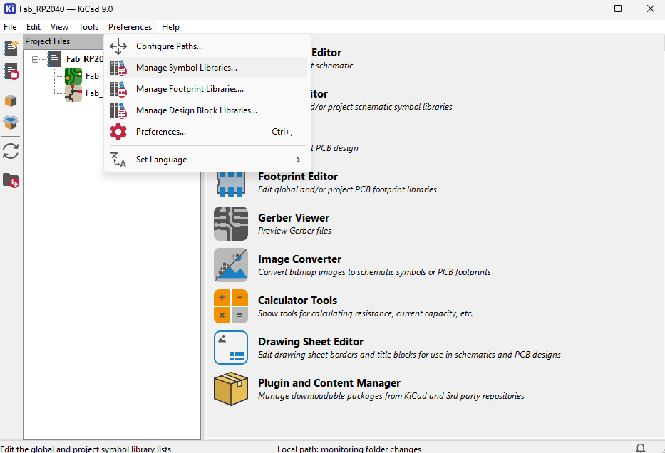
Step 9: Linking the Symbol Library
Now, from the KiCad program, it is necessary to link the symbol library so that it can be used properly within the schematic editor.
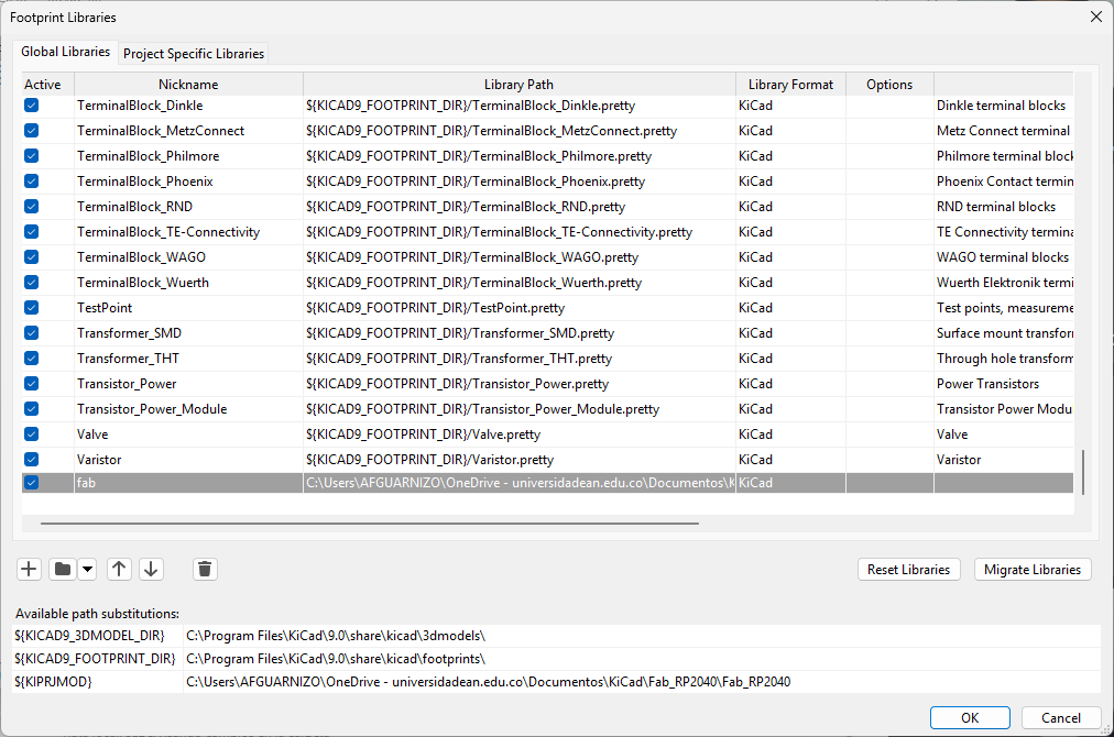
Step 10: Adding All Library and Project Paths
Finally, I added all the necessary paths for the libraries and the project files. This ensures that KiCad can correctly locate and use every component, footprint, and symbol across current and future designs.
3. Schematic Design
Once the project was fully configured and the libraries were correctly linked, KiCad launched the schematic editor. This is the primary workspace where all the electronic components will be placed and connected to start designing the custom board.
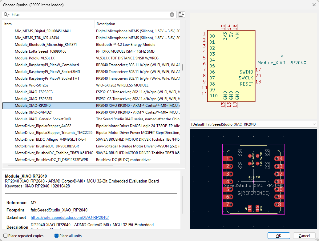
When clicking the button to add a component, I searched for the microcontroller board XIAO-RP2040. Once selected, KiCad displayed both its schematic symbol and associated footprint, which confirms that the previously linked libraries were loaded correctly.
I placed the XIAO-RP2040 board and also added the SMD (Surface-Mount Device) connectors, each with 5 terminals. These components are crucial for establishing external connections with other modules or sensors.
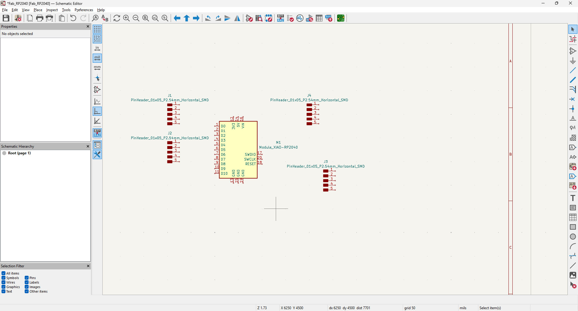
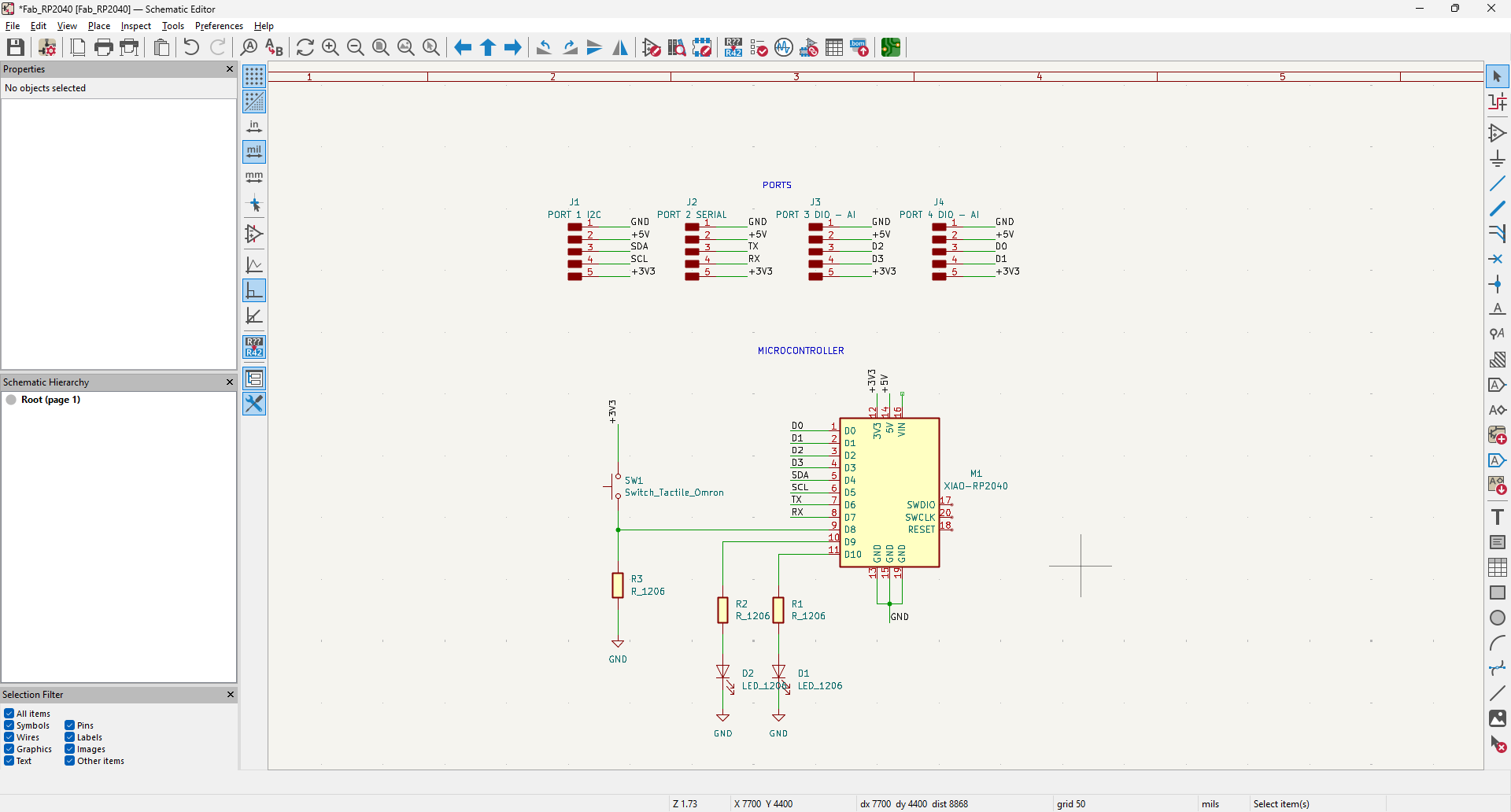
Finally, I placed all the required components in the schematic, including the ports, a push button, and two output LEDs. These will allow basic interaction with the board, simulating real-world input and output behavior.
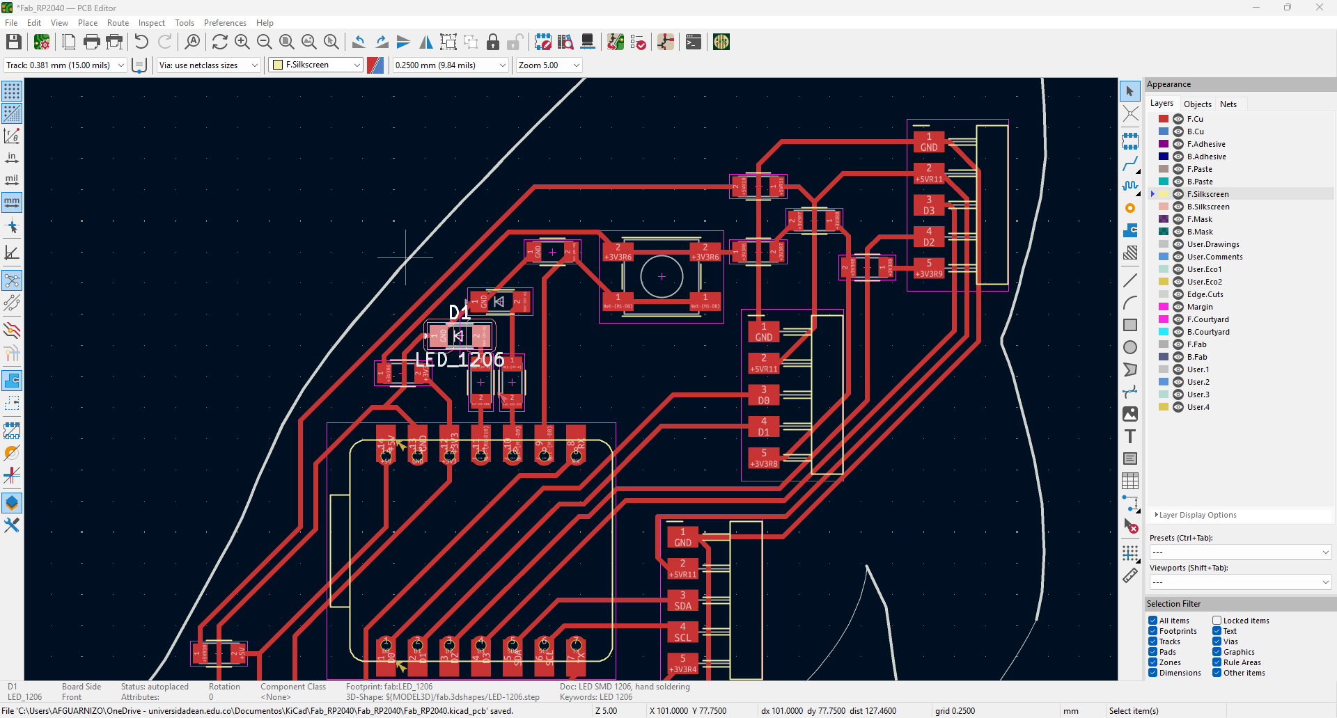
4. PCB Layout
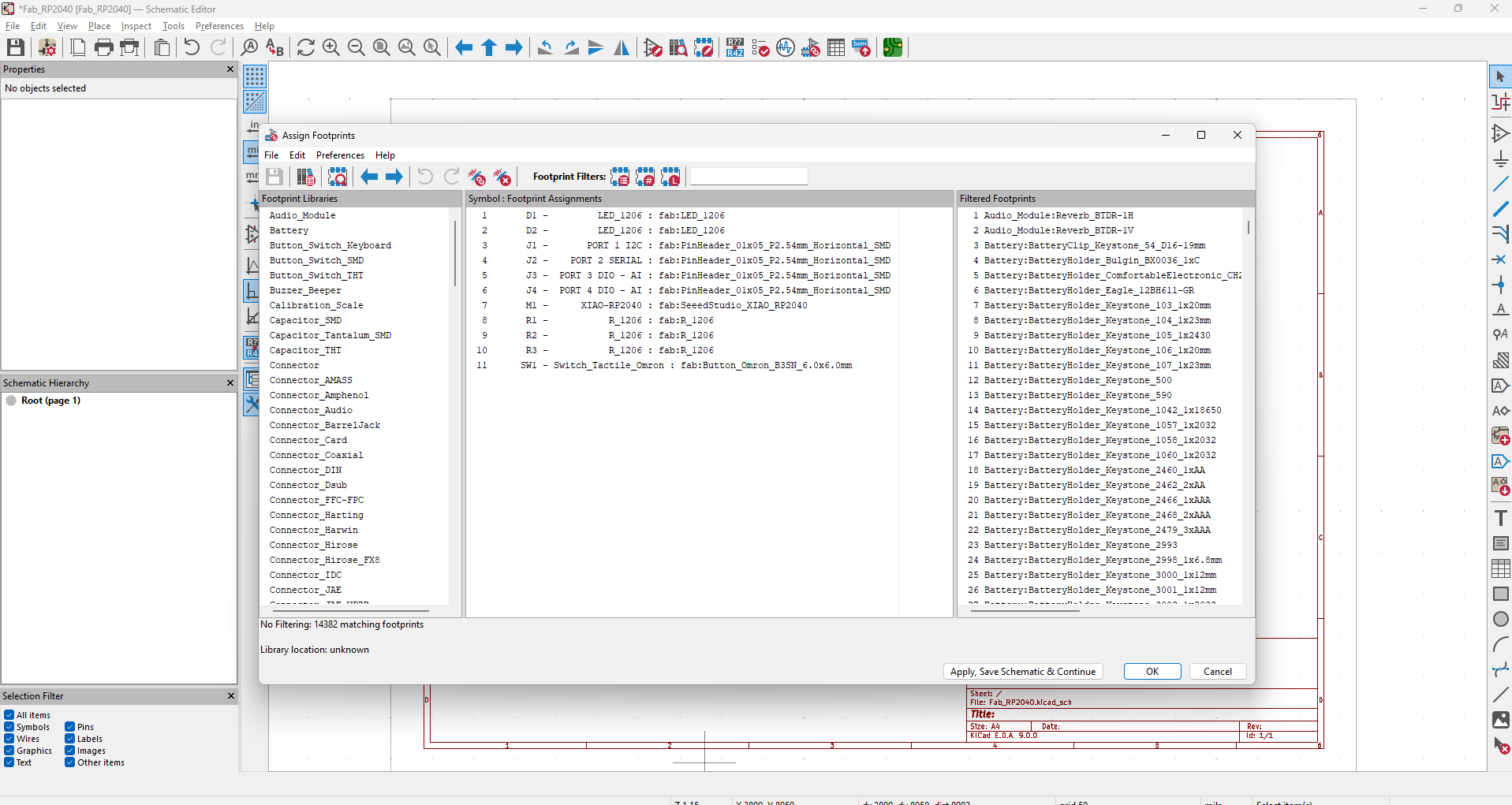
At the moment of selecting the option to create the PCB, the software requested that all component footprints be linked. I proceeded to assign the correct footprint to each component individually, ensuring consistency with the library previously loaded.
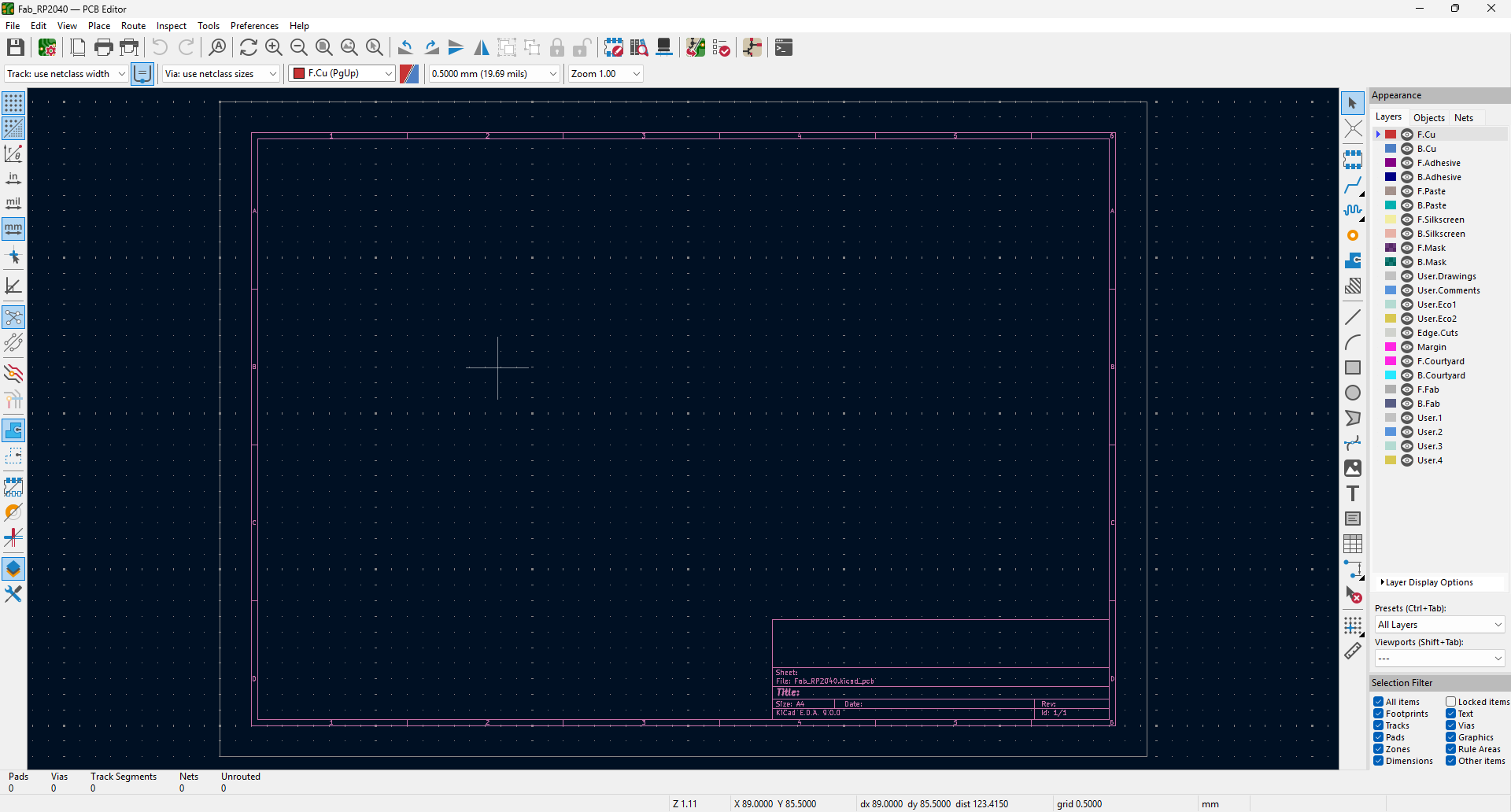
Finally, the PCB editor opens, allowing the placement and routing of all components on the board. This environment provides the tools needed to define traces, set board dimensions, and prepare the final layout for manufacturing.
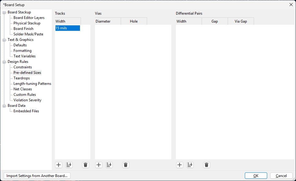
I added routing constraints by defining the track width rules. This ensures that all traces follow minimum width guidelines, which is critical for proper current handling and manufacturability. These constraints are part of the design rules set up before starting the actual routing process.
After many attempts and testing different routing methods, I struggled to generate proper traces. Whenever I tried to move or adjust a segment, the rest of the circuit shifted unexpectedly. This led me to explore new tutorials and techniques to better understand the routing workflow and improve my approach.
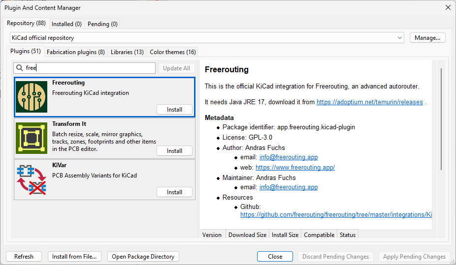
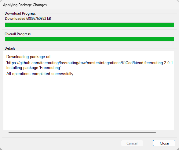
After searching online, I found a plugin for KiCad developed by a third party that enables automatic routing. The following images illustrate the installation process.
Then in KiCad, I added the previously installed Freerouting plugin to begin the automatic routing process within the PCB editor.
A confirmation message appeared indicating that the plugin had been successfully installed and integrated into KiCad.
After running the autoroute plugin, the tool generated a PCB layout with most of the tracks completed. Although the result looked acceptable at first glance, there were still some errors and warnings displayed in the message console that needed to be corrected. These errors and warnings are due to tracks that remain disconnected because the router could not find a feasible path. During the Saturday open time session, I learned that one possible solution is to use 0-ohm resistors as jumpers, which makes it easier to complete the routing and connect isolated traces efficiently.
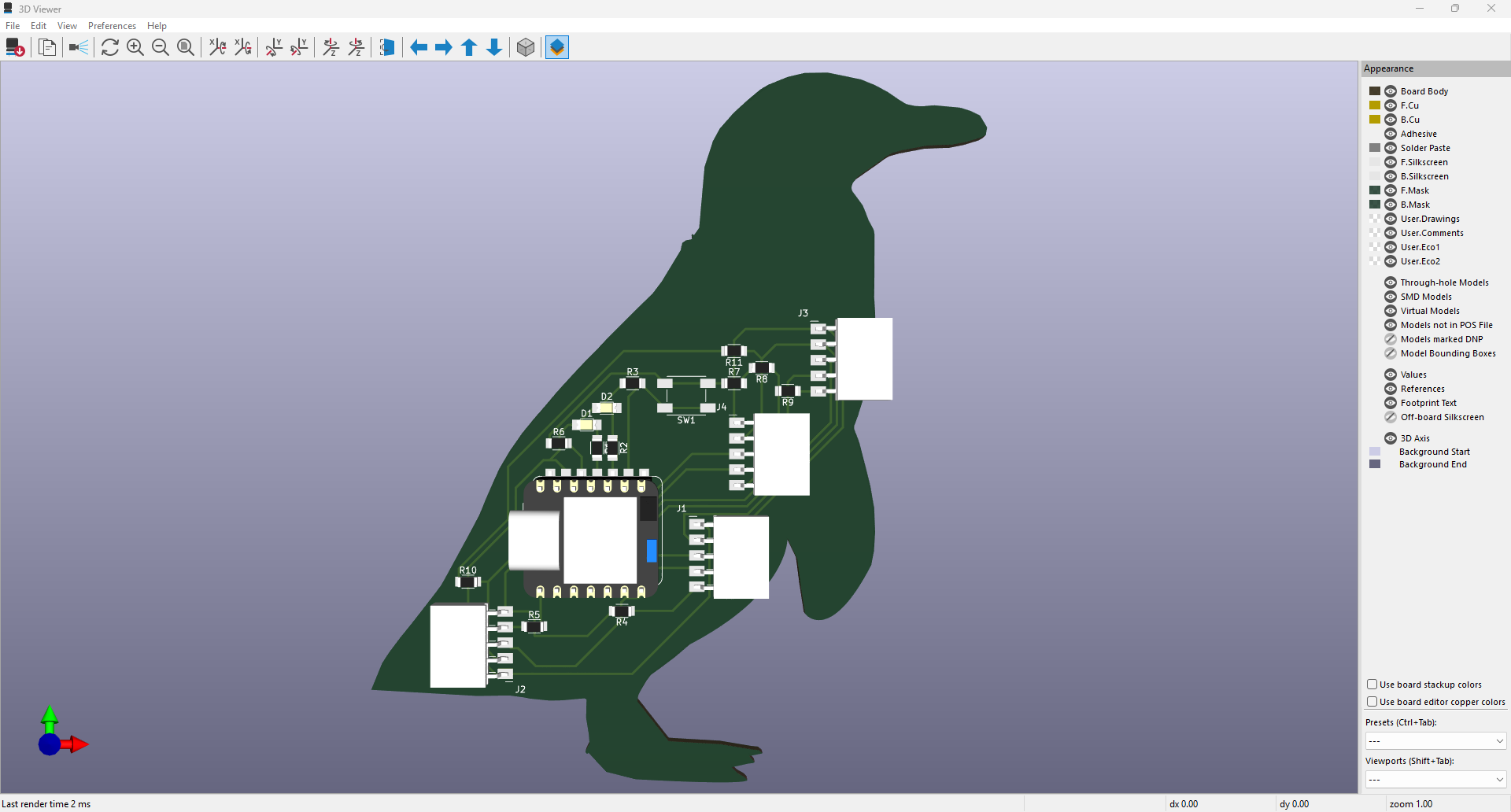
Once I had learned more about manual and semi-automatic routing, I decided to use the shape of a penguin to creatively organize all the components on the PCB layout. This approach not only allowed me to apply what I had learned in an engaging way, but also prepared the design for fabrication.
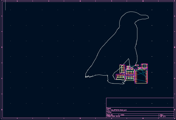
I preliminarily placed the components distributed across the penguin-shaped outline to begin the routing process. Component placement should be done strategically, anticipating potential issues or routing challenges that might arise later. This helps ensure that adjustments can be made more easily during the routing stage.
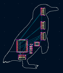
In the image below, the resistors used as jumpers can be clearly seen. These were placed to solve issues with interrupted traces, allowing connections to be completed where routing was not possible using only the top layer.
Finally, after assigning the correct footprints to the components that were missing them, improving the layout on the board, selecting the appropriate trace width, and resolving all previous errors and warnings, the final 3D result of the PCB can be seen below. This version of the design is clean, properly routed, and ready for fabrication without any outstanding issues.
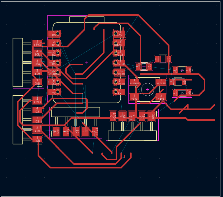
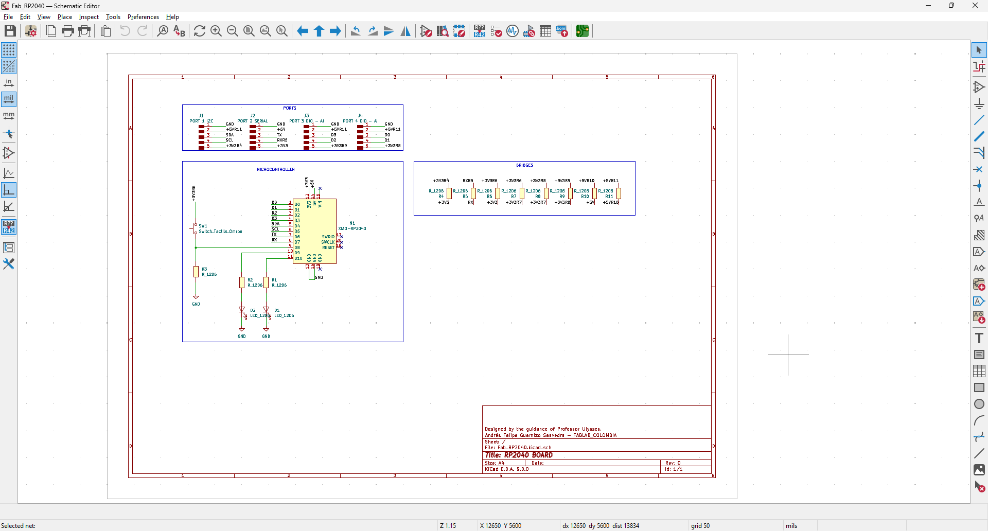
The final schematic, including the 0-ohm jumpers and improved organization of all components and connections, can be seen in the image below. This version reflects the finalized logic and wiring layout after multiple iterations and corrections.
Reflections
Working through the full design process of a custom PCB using KiCad and the RP2040 microcontroller was both challenging and enriching. Beyond simply placing and wiring components, it required understanding real-world constraints such as trace widths, component placement strategy, and how to resolve routing conflicts with 0-ohm jumpers.
Learning to use external libraries, plugins like FreeRouting, and integrating 3D footprints expanded my capabilities within KiCad. This experience also emphasized the importance of preparing clean and readable schematics, ensuring a more efficient transition to the layout phase and fabrication.
Ultimately, solving design rule violations and eliminating errors from the PCB validated my understanding of electronics design and gave me the confidence to move forward with physical board production. Designing around a creative shape like a penguin added an extra layer of fun and complexity to the project.
Extra Credit: Simulate Your Design
Since the RP2040 Zero is not available in Wokwi, the simulation was carried out using the Raspberry Pi Pico, which shares the RP2040 microcontroller. The goal was to simulate a simple digital logic behavior: when the button is pressed, the green LED lights up, and when it is released, the red LED lights up instead. The following video shows both the schematic and the MicroPython code working together in Wokwi.
MicroPython Code Used in Simulation
The following code was used in the Wokwi simulation to control the LEDs based on the button input:
                from machine import Pin
                import time

                button = Pin(15, Pin.IN, Pin.PULL_DOWN)
                led_green = Pin(16, Pin.OUT)
                led_red = Pin(17, Pin.OUT)

                while True:
                    if button.value():
                        led_green.on()
                        led_red.off()
                    else:
                        led_green.off()
                        led_red.on()
                    time.sleep(0.05)
Downloads and Project Files
The following files include the schematic, board layout, and 3D visualization assets for the custom PCB design using the RP2040 microcontroller. These files can be used to review the design, reproduce the fabrication process, or make improvements for future iterations.