Assignments
This week, we got hands-on with essential lab equipment like multimeters and oscilloscopes, learning how to probe and understand the behavior of microcontroller circuits. It was exciting to see those electrical signals come alive on the oscilloscope screen! My journey of mastering KiCad, an open-source EDA tool was more of a hellish experience as Designing my own circuit board for the ATtiny44 was really challenging. Yet it was a rewarding experience, filled with lots of persistence and resillience from my side. I was also able to connect my final project's soil moisture sensor and visualize its readings using the oscilloscope
Table of Contents
- Group Assigment
- Individual Assignment
- Final Project Development
- Unconnected pins: It will flag any component pins that haven't been connected to anything else in the circuit.
- Short circuits: It can detect if two or more pins that shouldn't be connected are directly linked.
- Power conflicts: If you have multiple power sources connected in a way that might cause a problem (e.g., two outputs trying to drive the same line to different voltages), the ERC can warn you.
- Input/Output conflicts: It can check if you're trying to drive an input pin with another input, or passively reading an output pin without a pull-up or pull-down resistor where needed.
- Missing power inputs: It can warn if a component that requires power doesn't seem to be connected to a power supply.
- Label conflicts: If you accidentally use the same label for different nets that are not intended to be connected, the ERC can point this out.
- The type of issue detected.
- The components and pins involved.
- Sometimes, a brief explanation of the potential problem.
- Select the "Edge.Cuts" layer: In the layer manager (usually on the right side of the PCB editor window), make sure the "Edge.Cuts" layer is active.
- Use the drawing tools: KiCad provides various drawing tools (lines, arcs, circles, rectangles, polygons) that you can use to define the shape of your PCB on the "Edge.Cuts" layer.
- Draw the outline: Carefully draw the desired outline of your board. Ensure that all your components and traces are within this boundary with sufficient clearance from the edge.
- Consider manufacturing tolerances: When designing the edge cuts, it's good practice to leave a bit of extra space around your components to account for manufacturing tolerances during the cutting process.
- Clarity and Readability: Instead of drawing long, potentially tangled wires across your schematic, you can simply place a label on a wire segment. Any other wire segment with the same label is automatically considered electrically connected, even if they are visually far apart on the page or on different sheets of a multi-sheet schematic. This makes your schematic much easier to read and understand.
- Organization: Labels help break down a large circuit into logical sections. For example, you might have a "POWER" label for all your power supply connections and separate labels for different signal lines.
- Reduced Clutter: By using labels, you avoid a "spaghetti" of wires crisscrossing your schematic, making it easier to follow the signal flow.
- Net Identification: Once you move to the PCB layout, the labels become the names of the electrical nets. This helps you understand which pads and traces need to be connected.
- Local Labels: These labels create a connection only within the current schematic sheet.
- Global Labels: These labels create a connection across all sheets in a multi-sheet schematic. They are particularly useful for power and ground connections that are used throughout the design.
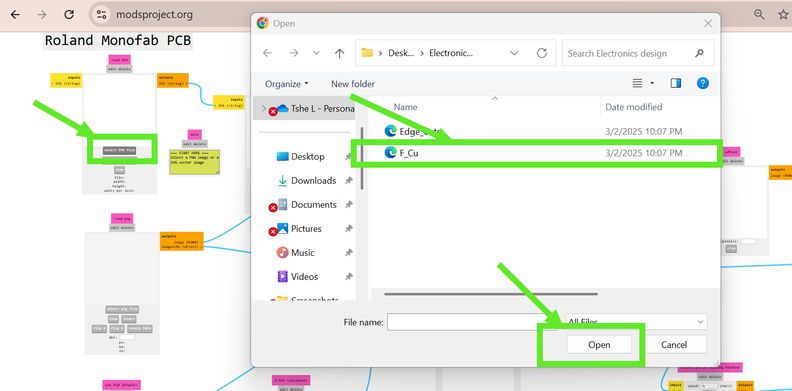
- Insert an SVG or PNG file (we will use an SVG file).
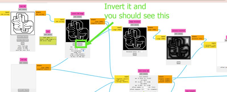
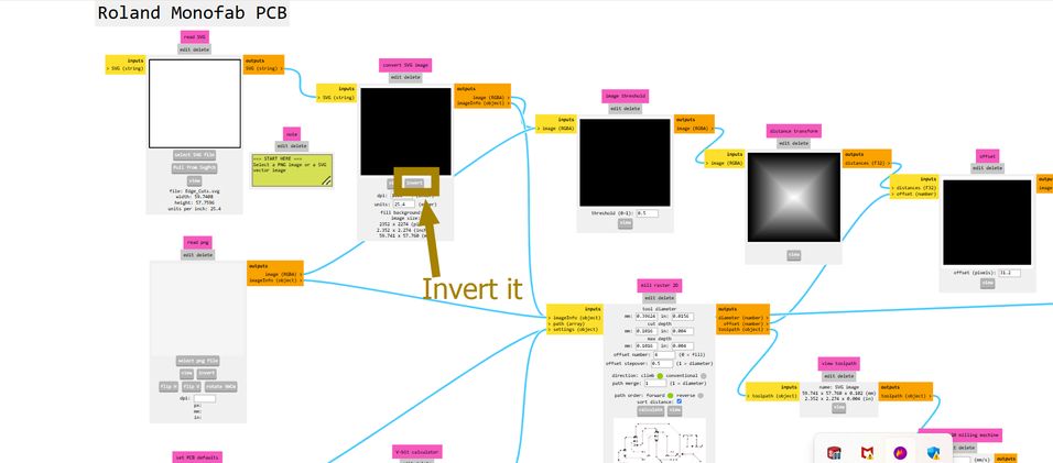
- Invert the image.
- Inversion is necessary because the software interprets black areas as regions to **preserve** and white areas as regions to **mill away**.
- By inverting, the traces remain intact while the surrounding copper is removed.
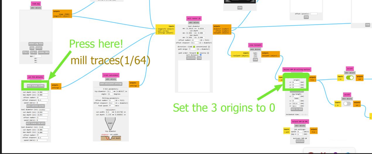
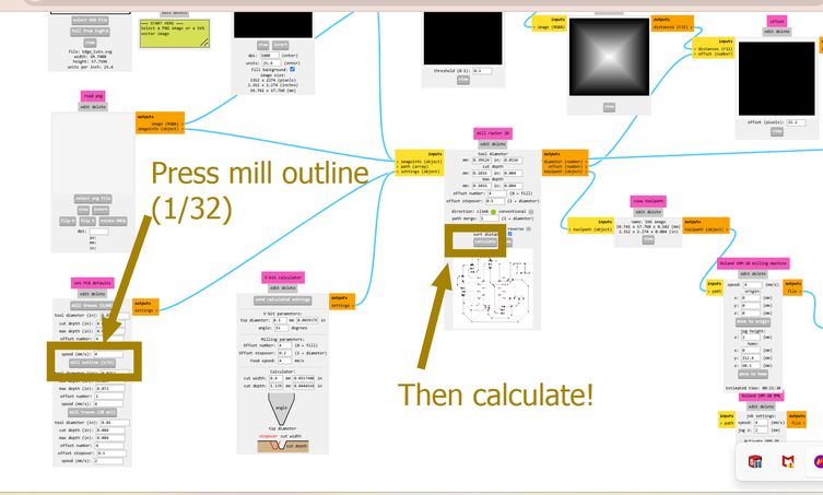
- Select "Mill traces by 1/64 inch" since we are using a 1/64-inch endmill for copper cutting.
The same procedure applies for edge cuts, except in STEP 3, where you must select "Mill with 1/32 endmill" as we will be using that for edge cutting. - Set all axes (X, Y, and Z) to 0.
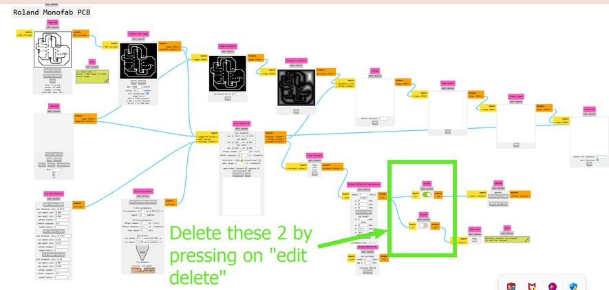
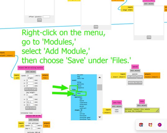
- Delete two unnecessary items (which are on/off elements and you can delete them by clicking on "edit delete"), then right-click and select Add Module.
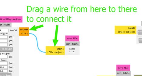
- Go to Files, click Save, and connect it to the Outputs file.
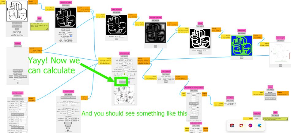
- Press "Calculate", and your RML file is ready to print!
Roadmap
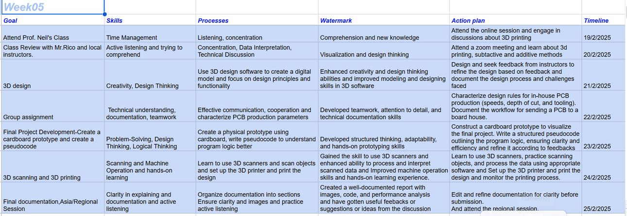
As I have become used to it, i started my week by creating a roadmap planning my activities for the week. This week is electronics design week and I am very excited to design my very own PCB! yay!!! and the we also learned about some really cool machines such as multimeter and oscilloscope in our lab and I had loads of fun!!1
Group Assignment
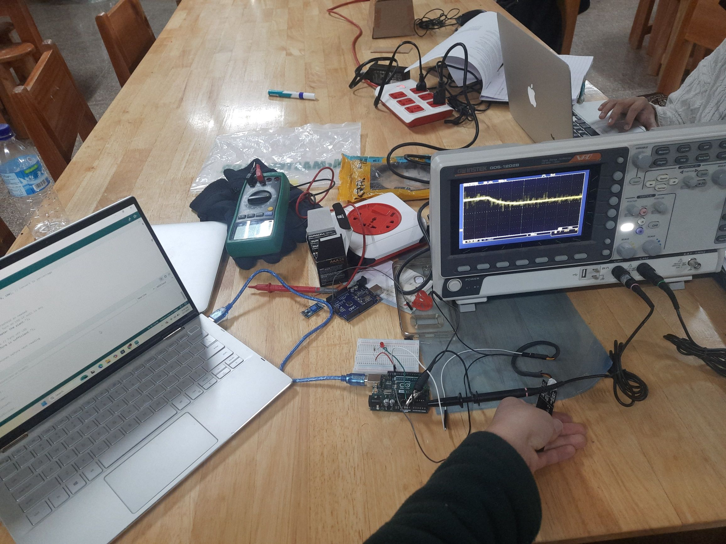
Use the test equipment in your lab to observe the operation of a microcontroller circuit board (in minimum, check operating voltage on the board with multimeter or voltmeter and use oscilloscope to check noise of operating voltage and interpret a data signal) Document your work to the group work page and reflect on your individual page what you learned
This week, we learned about oscilloscopes, which are tools used in electronics to see voltage changes over time. They work by converting electrical signals into visible waveforms on a screen. We explored the functions of a specific oscilloscope model and connected it to a microcontroller board to understand circuit behaviors better.
We also learned about multimeters, which measure voltage, current, resistance, and continuity in circuits. They work by applying known values and using Ohm's Law(V=IR) for calculations. We looked at the buttons and functions of a typical multimeter and learned how to connect it properly to circuits for accurate measurements. You can learn more about the group assignment here
Individual Assignment
During our pre-fab time, we were introduced to the basics of KiCad. Thus I decided to continue to learn and master this software.
KiCad is an open-source tool for designing electronic circuits and Printed Circuit Boards (PCBs). It allows users to create electrical schematics and seamlessly transition them to designing the physical layout of PCBs, ensuring accurate component placement and trace routing.
Libraries in PCB designing, libraries store schematic symbols and footprints, representing electrical components and their physical layout on the board. These collections make sure that your components are consistent and you don’t choose the wrong one by accident across projects.
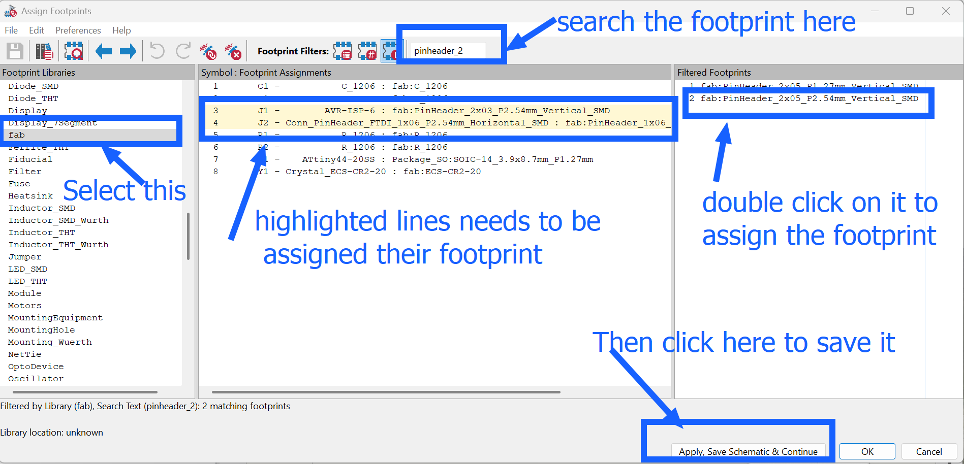
Footprints represent the physical layout of electronic components, defining their actual size, shape, and pad placement for soldering. Accurately matching your footprints to your schematic symbols makes sure that your electrical connections are correct and your physical components are compatible during soldering.
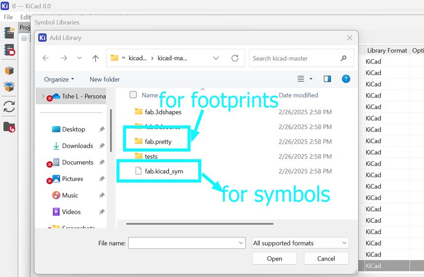
Adding libraries in KiCad. To add libraries in KiCad, first download your desired library. For my board I downloaded the library from this link. You have to press on the "code" and then under the download source code select "zip". Then you download it and extract it in your mac/pc.
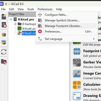
Now open Kicad and in the project window tap on preferences and choose either symbol library for components and footprint library for components' footprint.
After that you have to choose and select the folder icon as desired and add the downloaded library.
Learning Electronics Designing
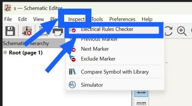
To learn electronics designing, I referred to boards in the fab academy website's and chose atiny44's boardWhile designing my schematic, I found it quite easy. I just had to create a new project and open the schematic editor. Then, I added the ATtiny44 component, connected VCC and GND, and placed a 0.1µF capacitor for power stability. I included 10kΩ pull-up resistors for the reset pin and I2C lines if needed. For the oscillator, I connected a crystal along with two capacitors to GND. Next, I added input/output components like LEDs (with resistors) and buttons, and wired a serial communication interface (FTDI for serial communication). For programming, I included an ISP header. Using the wire tool, I ensured all connections were properly made, then I annotated the components and ran an ERC check to identify any errors. The Electrical Rule Checker (ERC) is a powerful automated tool within KiCad's schematic editor. Think of it as a digital proofreader for your circuit design. Its primary purpose is to identify potential electrical issues and design errors before you move on to the PCB layout phase. This can save you a lot of time and frustration by catching problems early. The output of the ERC is usually a list of warnings and errors. Each entry will typically tell you: Based on this output, you would then go back to your schematic and modify the design to correct the identified issues. For example, if the ERC reported an unconnected pin, you would draw a wire to connect it to the appropriate part of the circuit. If it reported a power conflict, you would need to rethink your power distribution strategy. It's an iterative process – you run the ERC, review the output, make changes, and then run the ERC again until you have cleared all critical errors and understand any remaining warnings.
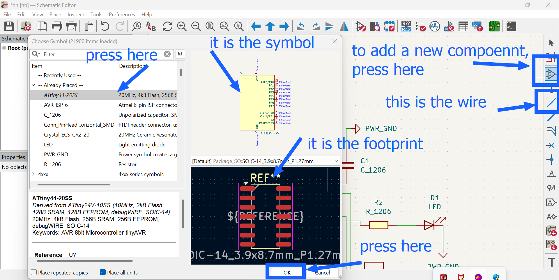
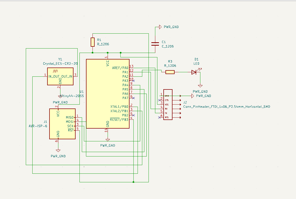
Electrical Rule Checker (ERC)
Common Issues the ERC Checks For:
Output and Modifications:
Then save the schematic and assign footprint.
And proceed to PCB design or export the netlist.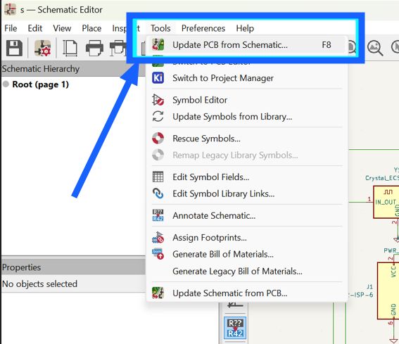
Making the PCB
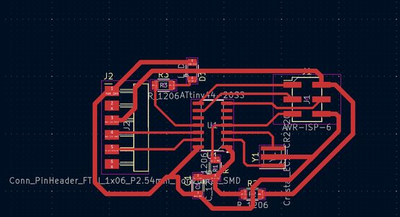
This task was hellish and I faced multiple setbacks. I designed the PCB almost 10 times and I was very frustrated by the time I was done. PRO TIP: keep on doing it until you get used to it. My 1st failure took me about 1 hour and then I designed others in 10 minutes each and failed multiple times.
At first I did not consider the different thickness of wires. It is 0.8 mm for all VCC and GND connections and 0.4 mm for all signal connections.
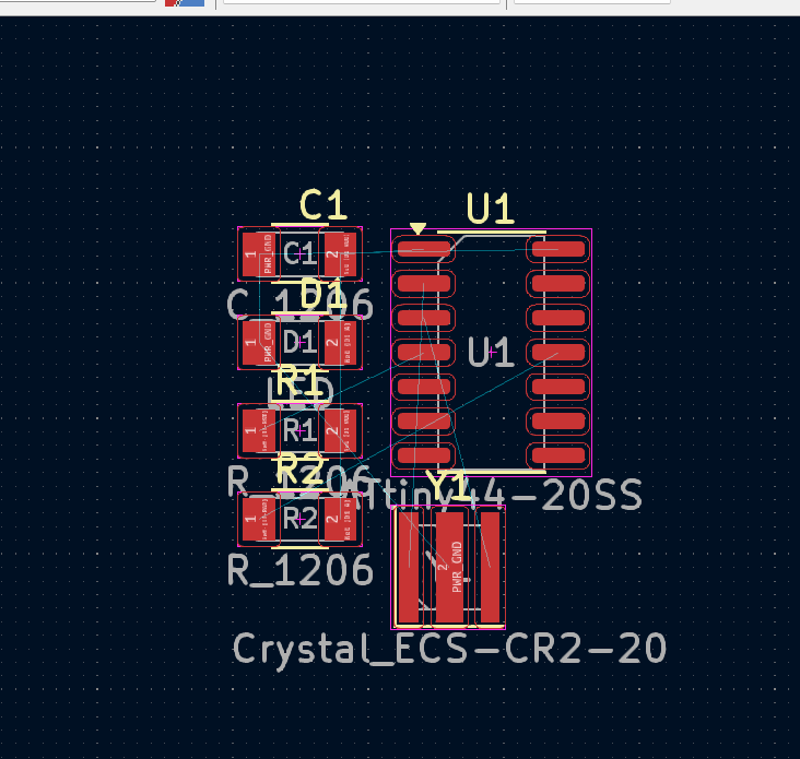
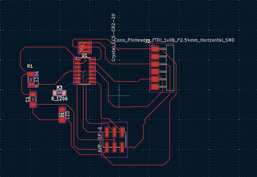
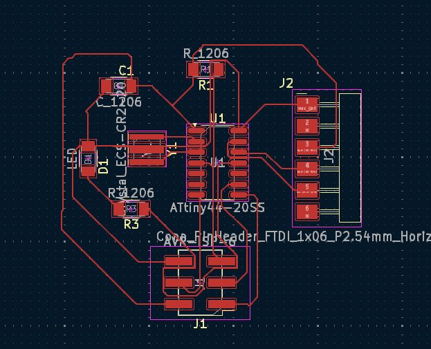
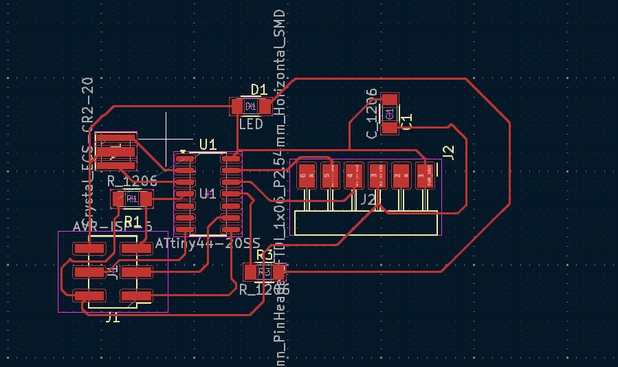
After I learned about the different thickness of the wires:
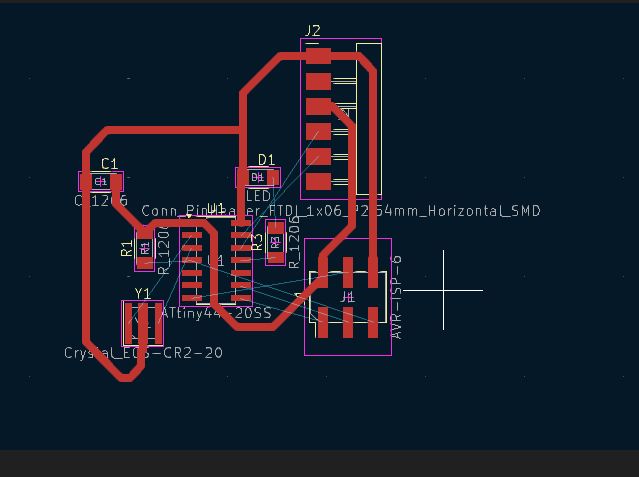
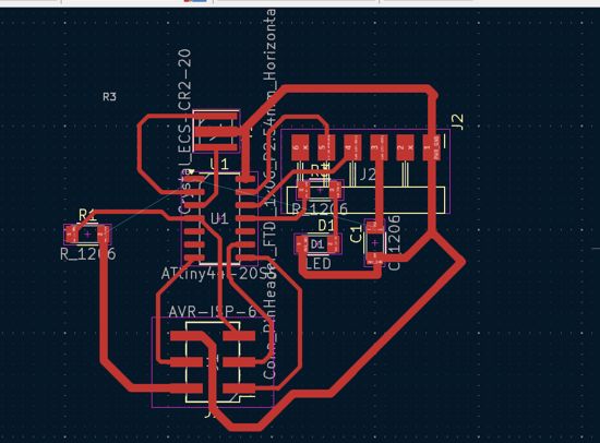
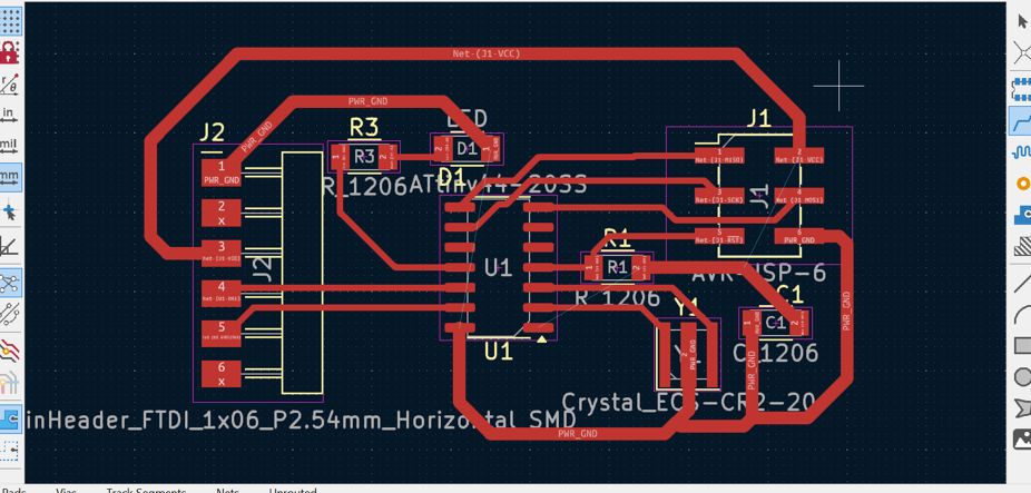
1 eternity later
Creating the Edge Cut
The Edge.Cuts layer in KiCad is specifically used to define the physical outline or border of your printed circuit board. Anything drawn on this layer will be interpreted by the PCB manufacturing process as the line where the board needs to be cut out from the larger material.
Here's how you typically create the edge cut in KiCad's PCB editor:
The shape you draw on the "Edge.Cuts" layer will be used to generate the outline for the milling or routing machine that will cut your physical PCB. I just created rectangle there.
The Actual Assignment
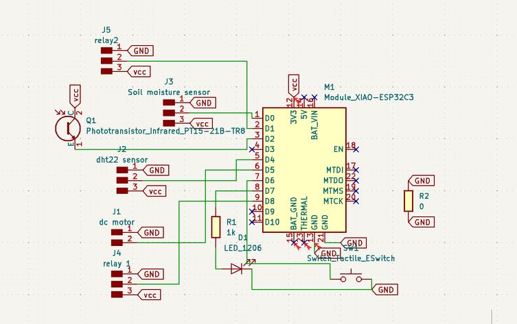
Now that I've learned electronics designing is a very cruel way, I decided to actually do my assignment which was to use an EDA tool to design a development board that uses parts from the inventory to interact and communicate with an embedded microcontroller. For it I wanted to create something related to my final projects board so I tried to create it. I was also imrpoving with my designing and making the schematic and PCB. I learned about labels this time:
Why Labels Are Useful:
Types of Labels in KiCad:
In my design, by using labels (like power and ground), i feel like I made the schematic much cleaner and easier to follow compared to a design with long, direct wire connections.
The schematic
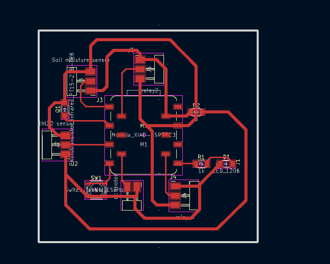
The PCB that I finished in my 2nd try because I got used to Kicad by now and Xiao is very simple too!! I recommend one and all to use it!!
Mods CE
Now that we are done with the schematic and pcb designing we must convert it to rml files. We convert PCB designs to RML (Roland Milling Language) files because RML is the format understood by Roland milling machines, such as our Roland SRM-20. The PCB design software (KiCad in this case) generates files in its own language(Gerber), which defines the circuit board layout, but these files must be translated into machine-specific commands for fabrication.
Firslt export the file as svg!
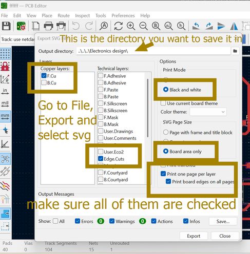
This is a very easy to understand and grasp user interface that I learned so to make it easy for others, I have explained it below.
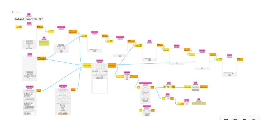
First of all, go to MIT MODS. Then right click -> Programs -> Open Program -> Roland (SRM-20 mill 2D PCB)-> Select svg
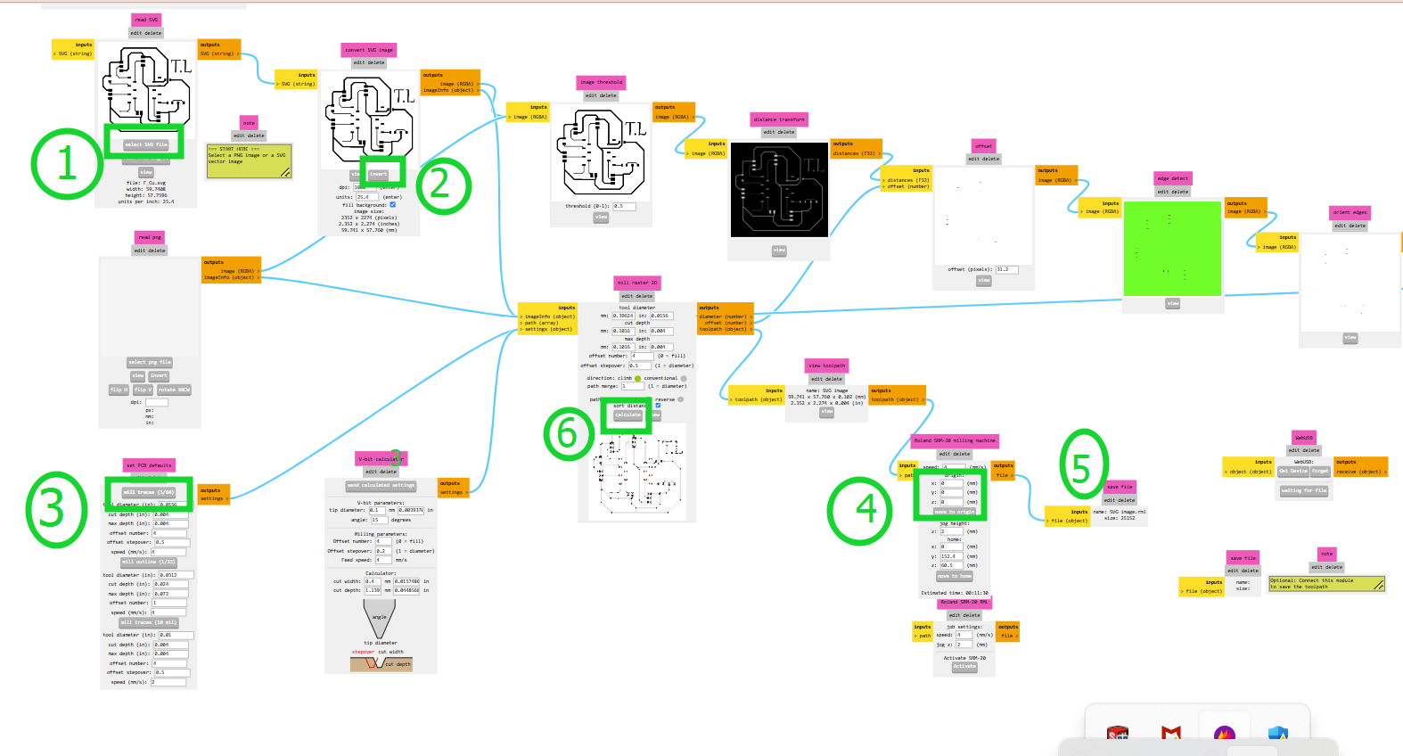
A more detailed explanation is here: follow these instructions
Right-click> programs> open program> mill 2D PCB

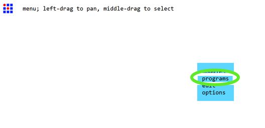
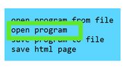
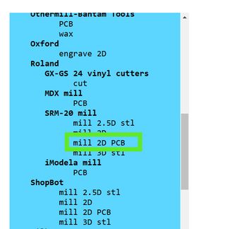
Then this should appear
Import the svg file and then invert it. We have invert it when generating toolpaths for PCB milling because the milling process is subtractive, meaning the machine removes copper rather than adding material.
Then we have to select mill traces 1/64 becasue 1/64 bit is used for copper layer isolation, as its tip is 0.4 mm that allows precise milling of PCB traces without damaging them. The 1/32 mill bit is used for edge cuts because its larger size which is 0.8 mm enables faster and stronger cutting, making it ideal for defining the PCB's outer shape.
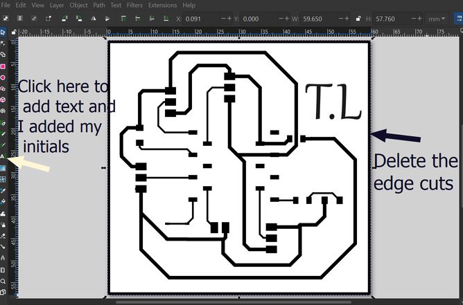
Oooops! Late Realization!! I forgot to add my initials on the board. SO I repeated the entire process again!
Now you must go to Inkscape, import the svg file and edit it. Then you have to save it.
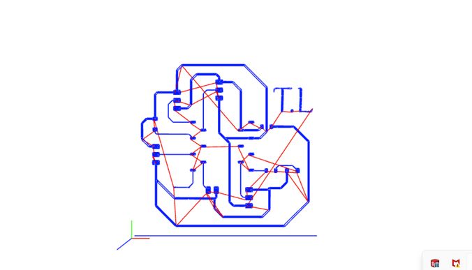
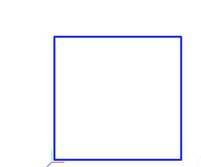
And this was the output!! This image helps visualize where the tool will cut, ensuring proper trace isolation or edge cutting. It also allows users to check for errors before sending the RML file to the milling machine.
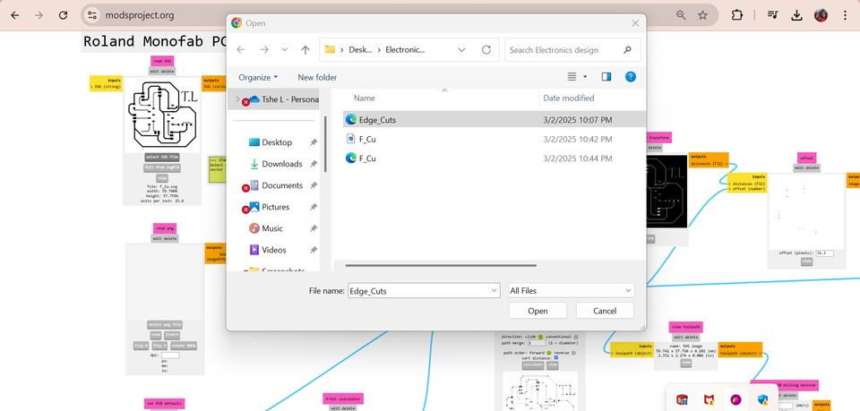
Similar to how we converted the copper layer to RML files, now we have to do it for the edge cuts too
Final Project Development
This week we connected the jumper wires to the breadboard, resistor, led and the arduino board. Then we asked AI-chatgpt to generate a code for arduino uno interacting with a soil moisture sensor and to blink the led if it is below a ceratin threshold. Then we connected it to the signal and GND of oscilloscope and observed it and WOW!!! It helped me visualize it better.
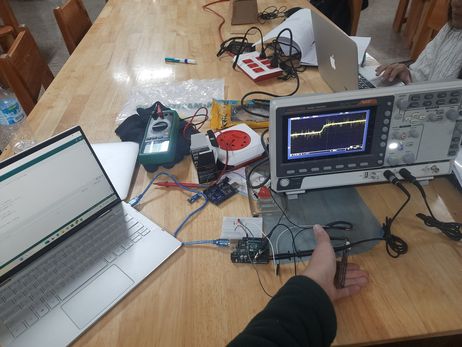
This is a video of it. The surge in the oscilloscope indicates that the soil moisture sensor has detected more moisture. We connected the FTDI with a USB cable to my pc and opened Arduino Ide and then copied and pasted the code there, then we went to sketch > Upload > Arduino Uno and then the code was sent there.
Reflection
This week taught me lots of new cool stuff but most importantly it taught me life skills such as resillience and rigour as I never gave up while designing my PCB for Attiny44 which was very frustrating and time consuming for me. However it was because I was a beginner using this software so it took me some time before getting comfortable and used to it.
I also made some progress regarding my final project which made me extremely happy!! I got to test my soil moisture sensors reading in oscillator which was enjoyable. It was a great experience this week.
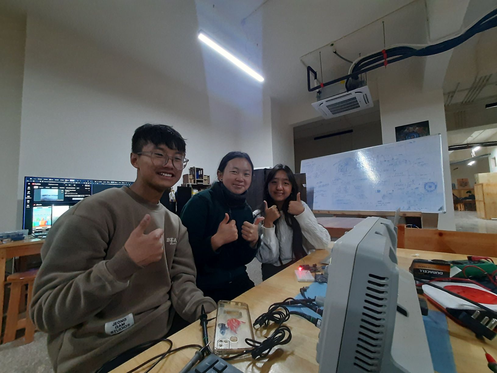
✅ Kudos to our great assistant instructors: Dawa Seldon and Yangtshel Wangyel for all of their help.
Files
You can access the files here
Final Project Board
Attiny44 Board
svg files for final project board
svg files of Attiny44 Board
Kicad files
