This week I was very excited to organize my time to make a piece of furniture that I can use as a help table for soldering and welding.
WEEK GROUP
SDS7202 Oscilloscope
Group assignment
Global
KIcad
Individual assignment
Conclusions
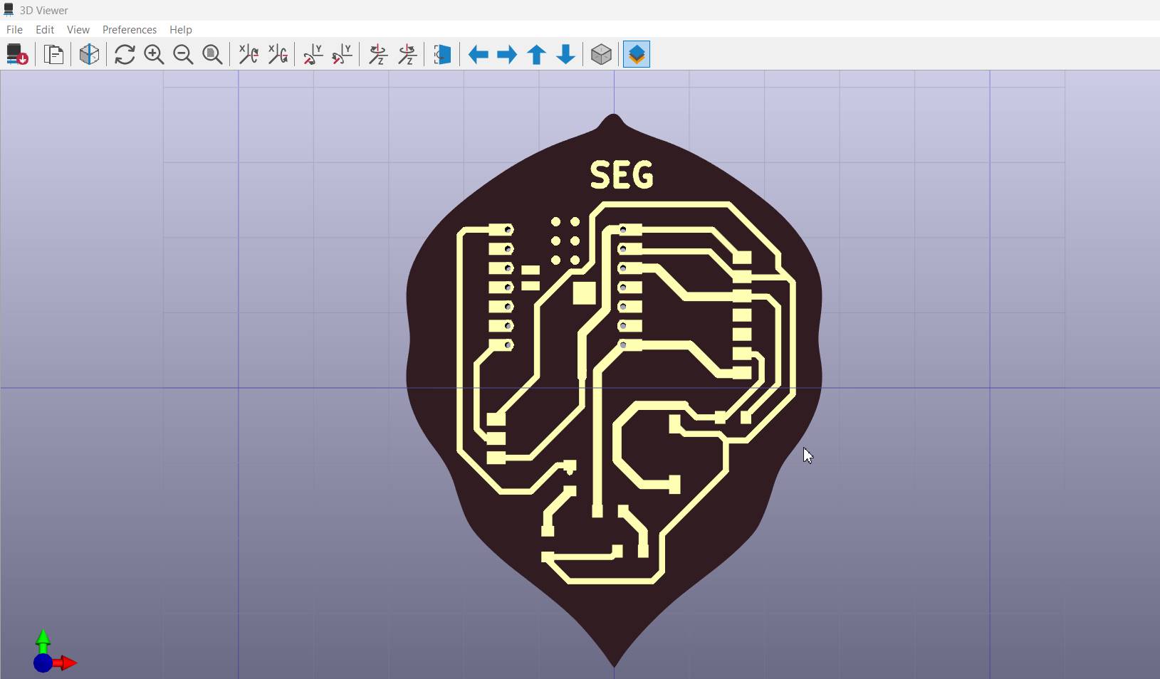
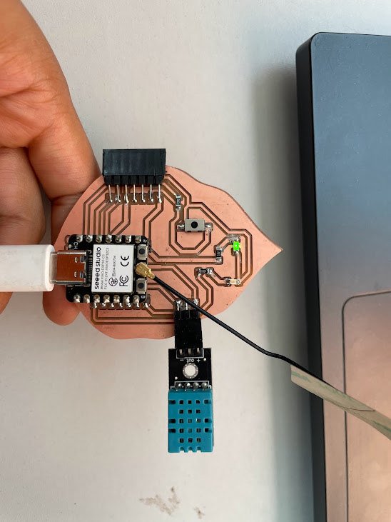
This is the final result
Our tasks for this week are:
Group assignment:
- Use the test equipment in your lab to observe the operation
of a microcontroller circuit board
send a PCB out to a board house
Individual assignment:
-
Use an EDA tool to design a development board to interact
and communicate with an embedded microcontroller,
produce it, and test it
- Extra credit: try another design workflow
- Extra credit: design a case for it
- Extra credit: simulate its operation
SDS7202 Oscilloscope

SDS7202 200MHz, 1GS/s, 2-channel+1-External, 10Mpts/Ch, 8″ Color LCD Display Deep Memory Digital Storage OscilloscopeThe OWON Smart DS Series Deep Memory Digital Storage Oscilloscopes are developed based on 8-bit with 2 channels simultaneously plus 10Mpts capability for each channel, enabling to capture and display signals of up to 300MHz with high 3.2GS/s sample rate. The SDS Series are the ideal and affordable DSOs for precise measurement and help identify and isolate problems for faster troubleshooting.
Characteristics
- Display screen: 8″ Color LCD display
- Bandwidth: 60MHz – 300MHz with dual-channel
- Max 300MHz bandwidth and up to2GS/s sample rate (SDS9302)
- Channel isolation: 50MHz : 100 : 1, 10MHz : 40 : 1
- Smart design and easy portability
- Waveform storage: 15 waveforms
- Available with frequency counter and FFT for all models
- Versatile interfaces: LAN and USBare provided as standard; RS232 and VGA optional
Experimenting with electronic equipment
Group assigments
March 3
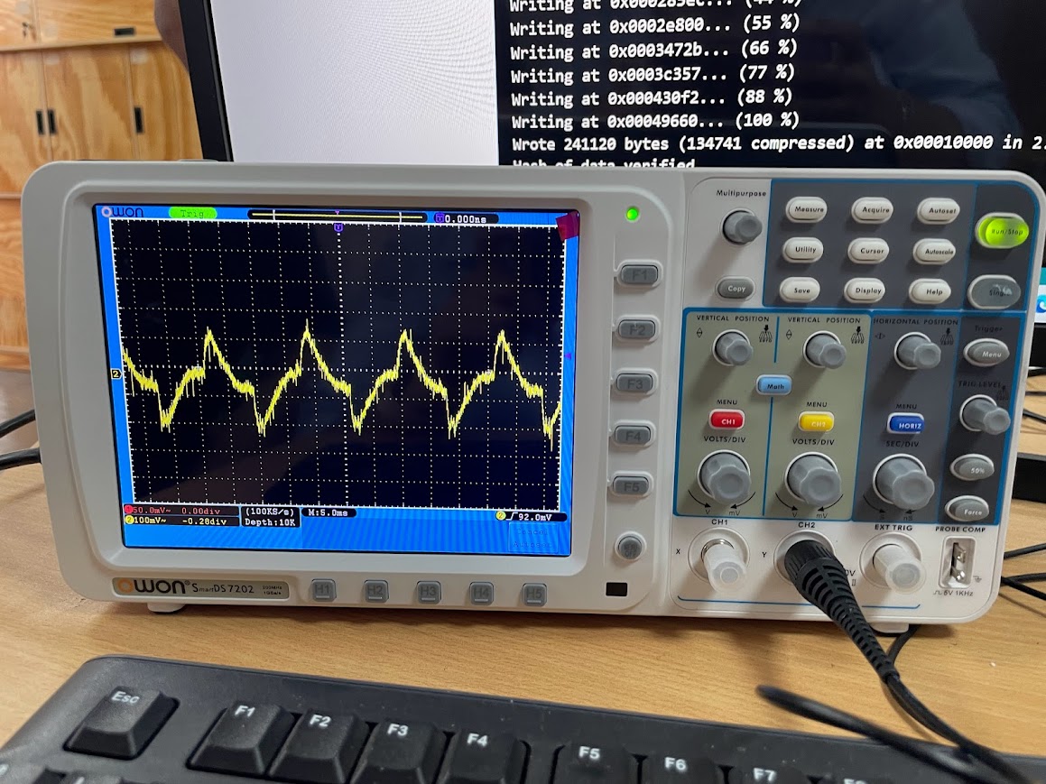
On March 15th, we visited IEST Simon Bolivar in Callao. Although the journey was lengthy,
it proved highly beneficial for our activities in week 8. We were able to utilize oscilloscopes to
test the functionality of our circuit boards. During testing, we discovered that some boards
were not functioning correctly, as indicated by the signals displayed on the oscilloscope.
Through this process, we were able to confirm that the errors were not due to issues with the
oscilloscope itself.
TRAINING
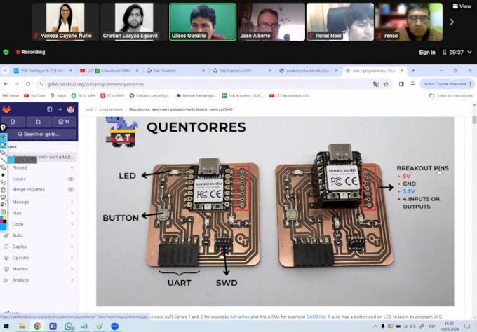
PCB design training by teacher Ulysses
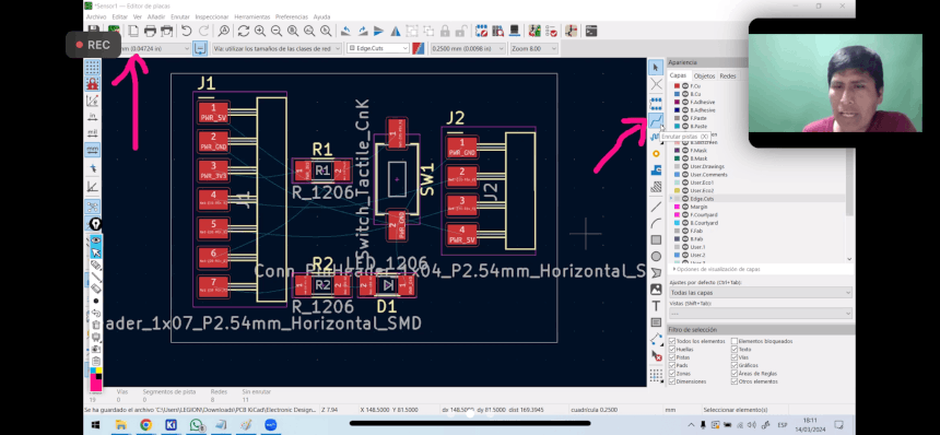
Kicad
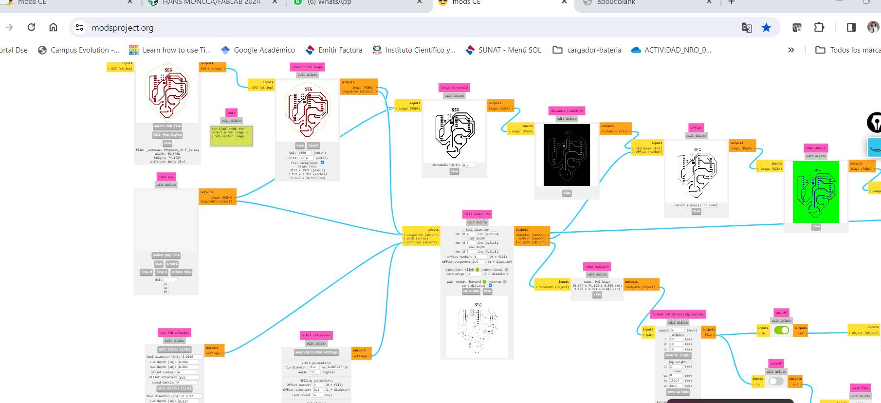
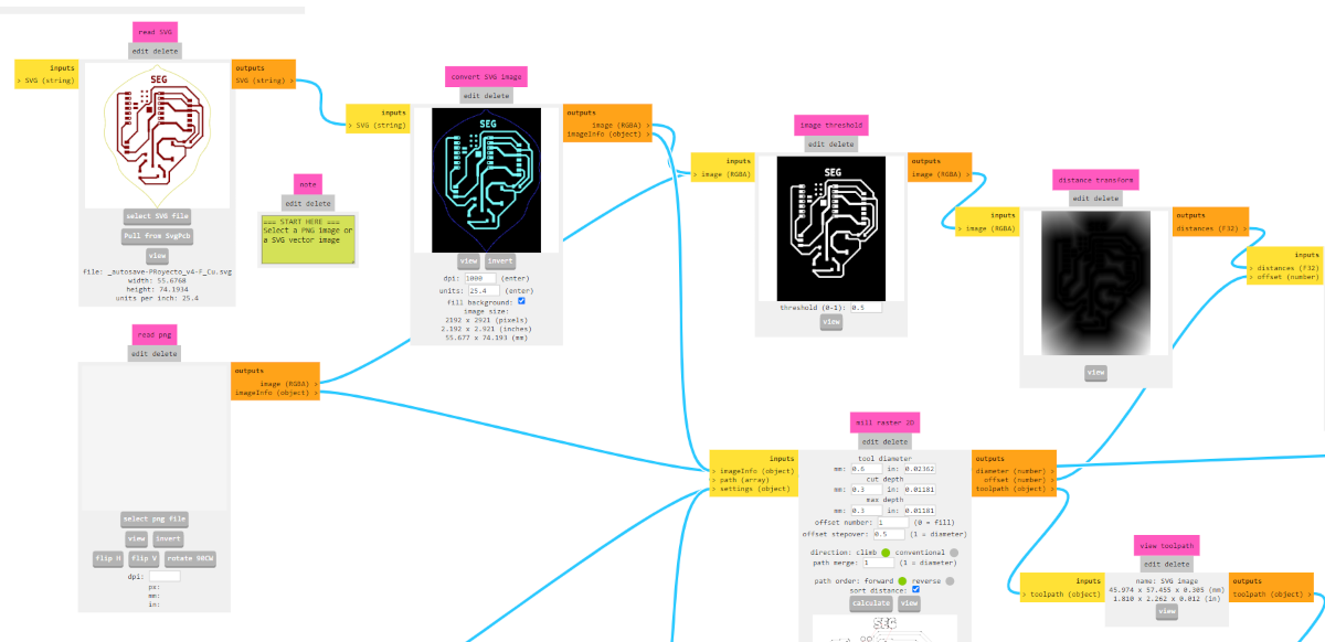
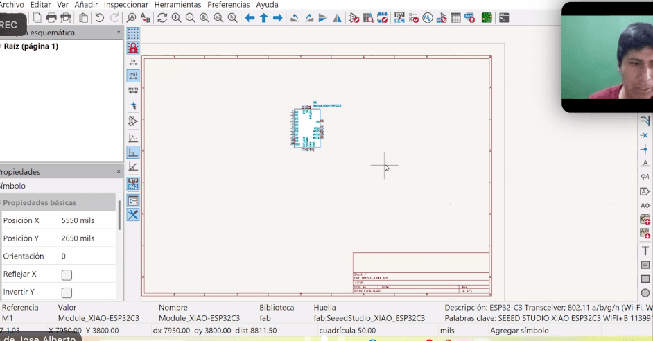
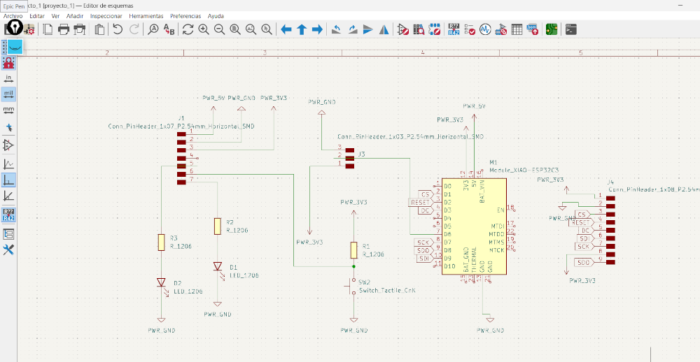
In KiCad, I can create and edit electronic circuit schematics with ease
To add components in KiCad, I first open the schematic editor. Then, I select the option to add a component, find the desired component in the library, select it and place it on the schematic by clicking on the desired locationy personnel so that they can respond effectively in the event of a medical emergency.

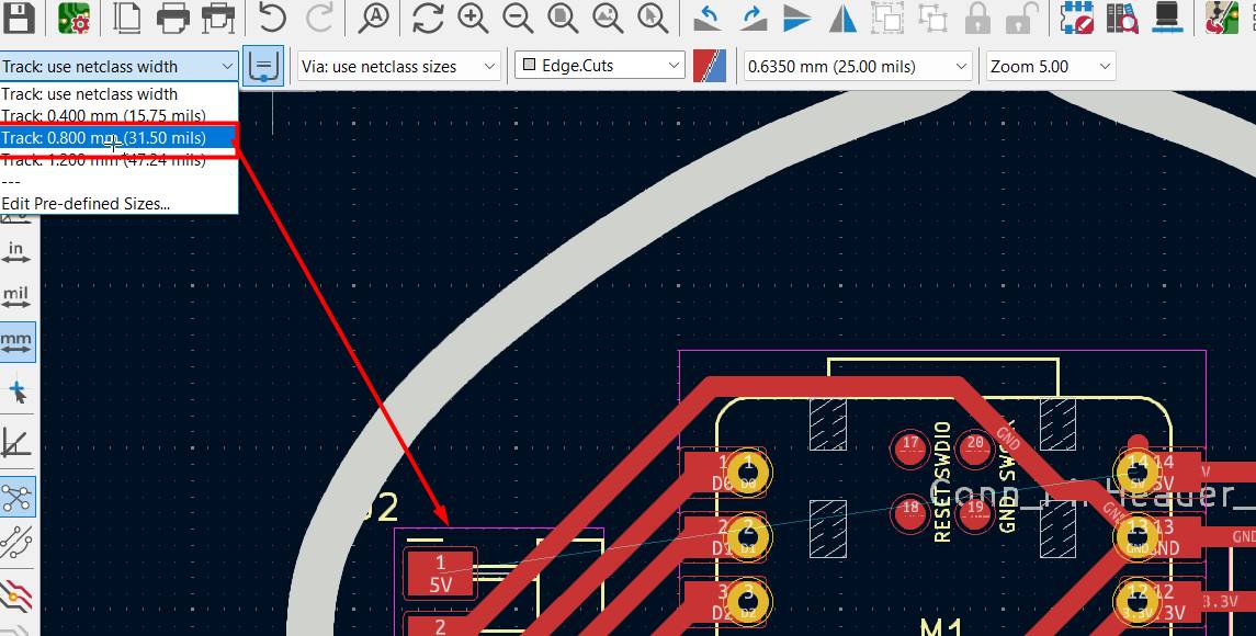
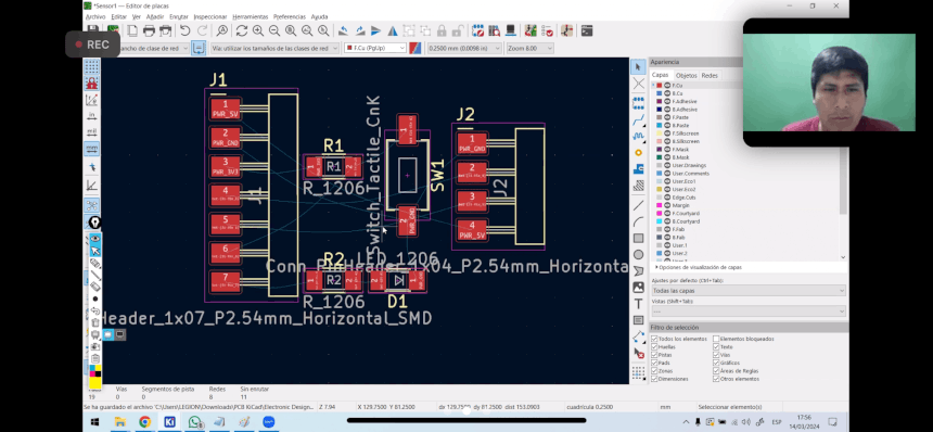
When designing a PCB in KiCad, we can visualize the shape of the tracks that connect the components before even soldering them.
This allows us to plan and design the routing of the tracks efficiently, ensuring that there is no interference or short circuits between the connections.
By seeing the shape of the traces, we can anticipate how current will flow through the circuit and ensure that the connections are strong and reliable once the components are soldered in place.
This is essential to ensure proper functioning of the circuit once the PCB has been manufactured.
I learned several important steps to do it correctly. First, we open a new project and enter the schematic editor.
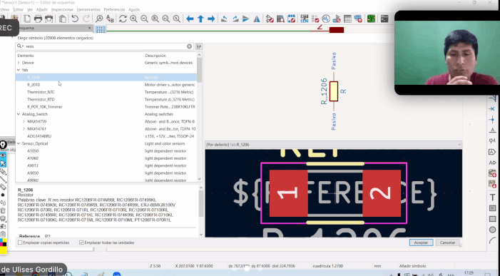
From there, we selected the components we needed from the KiCad library and placed them in the schematic work area.
Then, we connected the components using a specific tool and organized everything logically and neatly, labeling each element so it was easy to identify.
After checking and correcting any errors, we save our work and generate the necessary files.

Here we can see the components you placed on the schematic and how they are connected to each other.
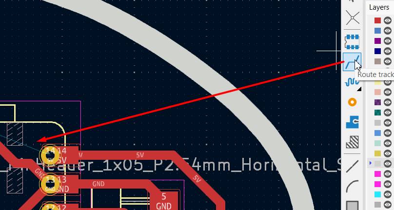
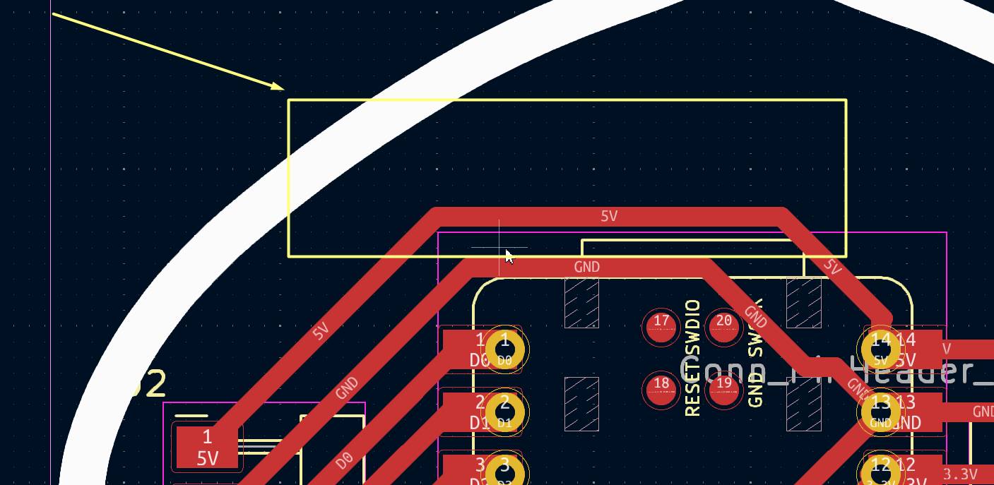
One of the most important things we learned was the importance of placing component connection paths efficiently. The professor explained to us that by carefully organizing the routes, we can minimize electromagnetic interference and ensure optimal circuit performance. He showed us how to use KiCad tools to plot routes in an orderly manner and avoid unnecessary junctions. It was really enlightening to see how routing decisions can affect the functionality and reliability of our design.
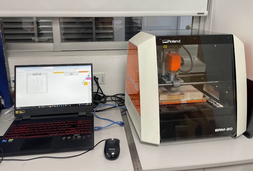
We met at the FAB LAB Universidad Científica del Sur to carry out our group work and also to move forward with our individual work. All with the knowledge of safety, to do a good job.
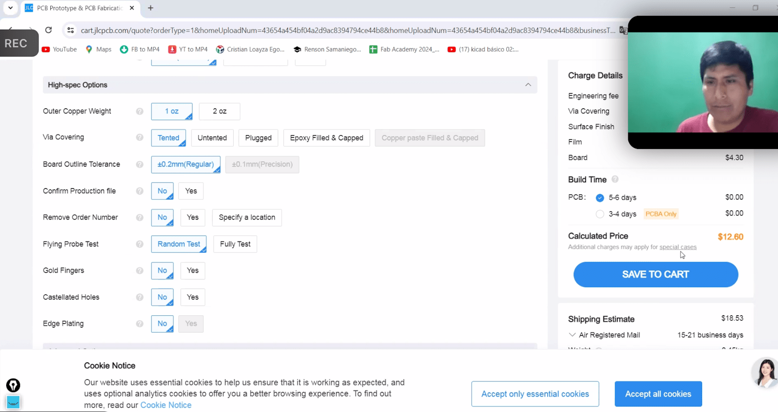
The photo shows the steps to send a PCB design to China for manufacturing. First of all, the importance of
preparing the files in a compatible format, such as the Gerber format, is highlighted,
which includes the information necessary for the manufacture of the PCB, such as the copper layers,
the solder mask and the silkscreen. Additionally, the need to generate a bill of materials (BOM) that
lists all the components necessary for assembly is shown. Another requirement is to specify the desired
quantities and characteristics of the PCB, such as material type, thickness, and surface finish. Finally,
the importance of communicating with the Chinese supplier to coordinate the sending of files and clarify any additional details before proceeding with manufacturing is highlighted.
Global Open Time

Saturday, April 16, we received a series of valuable tips to improve the design and creation process of our circuit boards. We were instructed on proper component selection and the importance of accurate soldering to ensure optimal performance.
Additionally, key aspects to consider during the creation of a PCB were highlighted, emphasizing the importance of efficient arrangement of elements and attention to detail to achieve successful results.
The SDS7202 oscilloscope has a wide variety of applications in various fields of electronics and engineering.
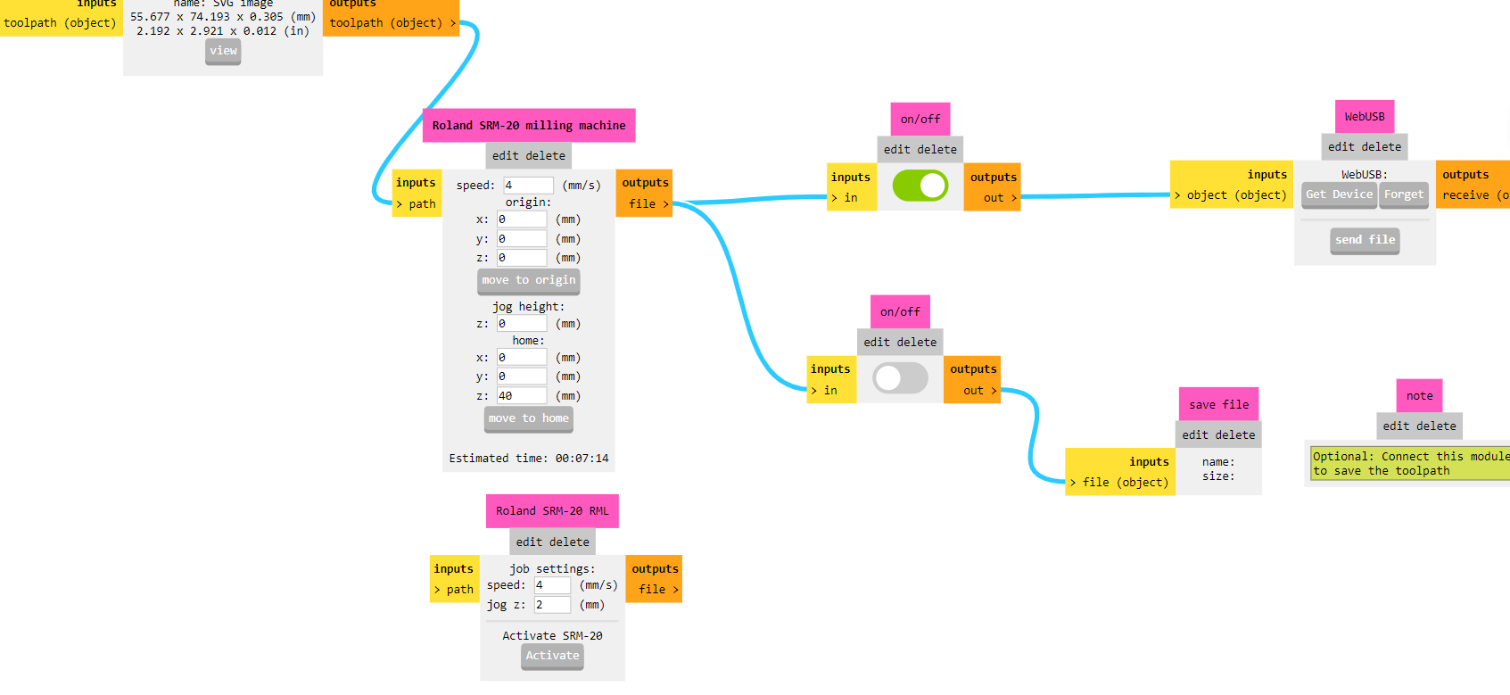
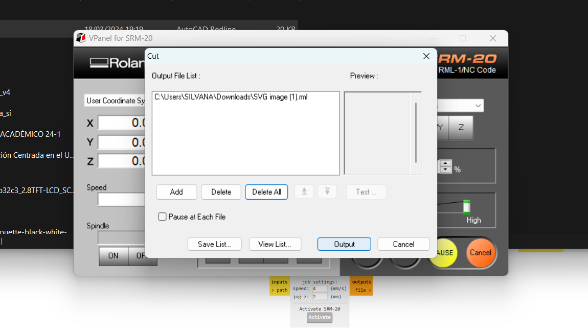
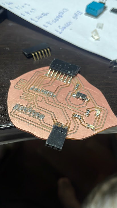
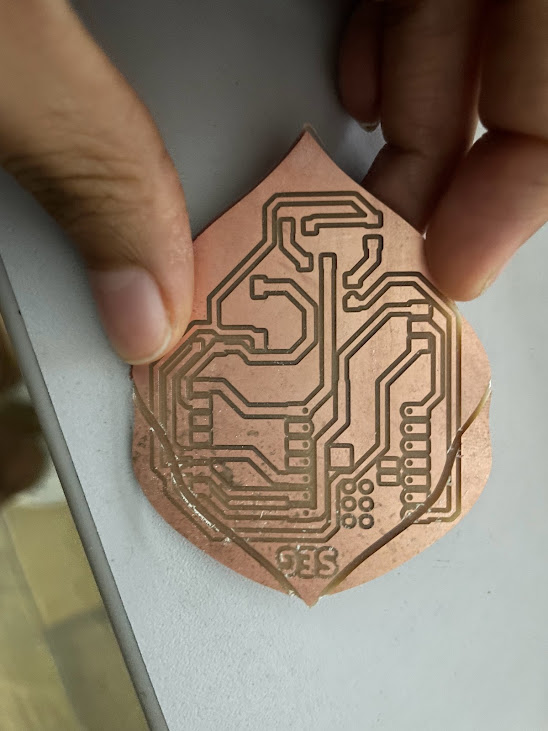
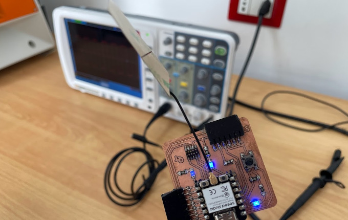
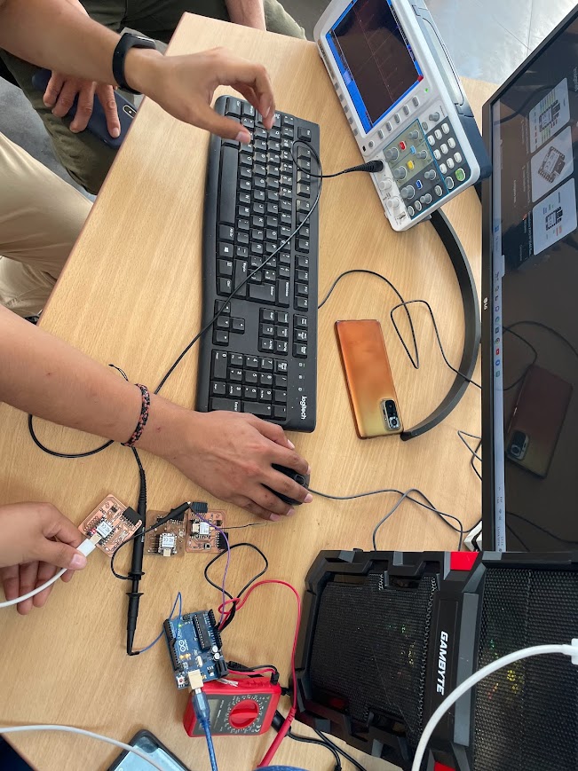
Here we were connecting everything and seeing what board we will use, in this opportunity we will use the one I made, to test if everything is ok in the tracks.
Debugging electronic circuits: The oscilloscope can be used to detect and troubleshoot electronic
circuits by providing a real-time display of electrical signal waveforms. This allows problems
such as distorted signals, electrical noise or connection errors to be identified.
Circuit testing and diagnostics: Useful for performing tests and diagnostics on electronic circuits
to verify proper operation and ensure they meet design specifications. This includes measuring
electrical parameters such as voltage, current, frequency and response time.
Channels CH1 and CH2 (or Channel 1 and Channel 2) are two independent inputs of the oscilloscope
that allow the user to measure two different electrical signals simultaneously. Each channel is usually
associated with a set of buttons and controls that allow their individual characteristics to be adjusted and configured.

Volt/Div" button: This knob allows you to adjust the vertical scale of the signal on the oscilloscope.
By turning this knob, you can change the number of volts per division on the oscilloscope screen.
This controls the vertical sensitivity and determines how much voltage each grid represents on the screen. Adjusting this parameter is crucial to properly display the amplitude of the signal you are measuring.
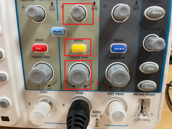
Menu" button: The "Menu" button gives you access to different options and settings of the oscilloscope.
Pressing it will usually open a menu on the oscilloscope screen that allows you to select different functions and settings.
From here, you can change the oscilloscope settings, such as time scale, coupling type, automatic measurements, etc.
Vertical" buttons: These buttons allow you to adjust the vertical parameters of the signal you are measuring on the oscilloscope.
They may include buttons for adjusting the voltage level, AC/DC/GND coupling, and the vertical position of the signal on the screen.
These controls are essential to obtain an accurate display of the signal and to adapt it to your specific measurement needs.

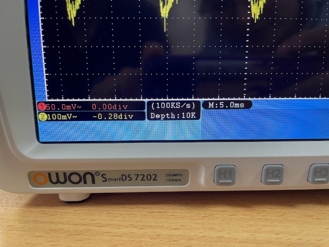
Here we first look at the schematic of the board to be able to know which track to measure, before doing so we
tested with an Arduino and a program called blink was placed in it to be able to know the changes that oscillate on pin 9
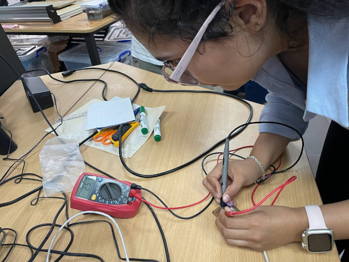
I measure the voltage of the LED to be able to know the amount of voltage, then measure the resistance, and test the continuity in the tracks.
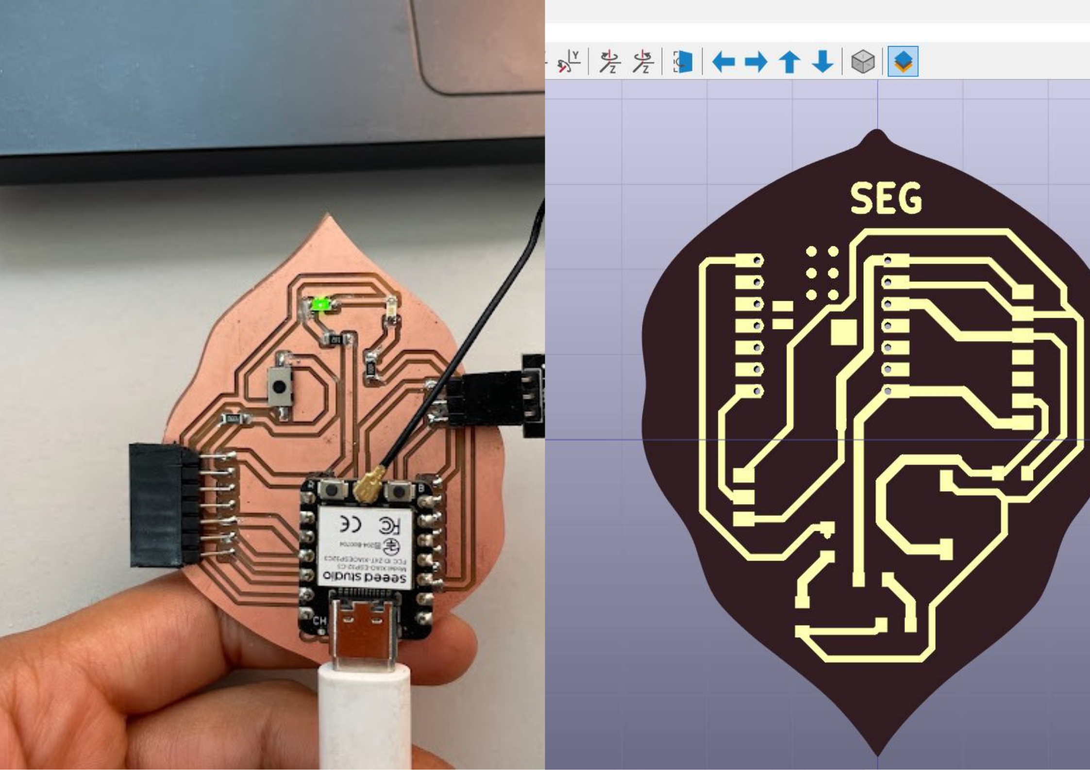
I utilized KiCAD to design . Although it was my first time using KiCAD, I found it relatively easy to learn the basic operations,
largely due to the helpful tutorial. Remarkably, I was able to generate my initial Gerber files within just one day.
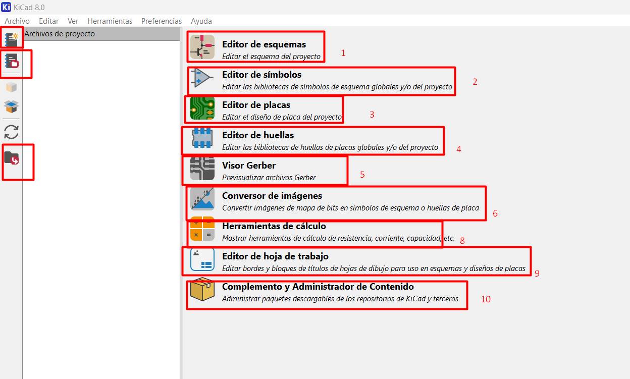
- Schematic Editor: This tool allows you to design and draw the electronic schematics of your circuits. You can add electrical components,
connect them with cables, and define functional relationships between them. It is useful for planning and visualizing how components
interconnect in your electronic design.
- Symbol Editor: The symbol editor allows you to create and edit graphic symbols that represent electrical components in your schematics. You can customize the appearance and properties of symbols to fit your specific design needs.
- Footprint Editor: This tool allows you to create and modify footprints or assembly patterns of components on the printed circuit board (PCB). You can define the dimensions, shape and characteristics of the solder pads, as well as the physical arrangement of the components on the board.
- Gerber Viewer: The Gerber Viewer allows you to view Gerber files, which are the standard files used to describe the layout of the print layers of a PCB. You can use this tool to check the appearance of your PCB design before sending it to manufacturing.
- Image Converter: This tool allows you to convert raster images (such as BMP, PNG, JPEG files, etc.) into vector formats that can be used in your PCB design. This is useful for including logos, graphics or drawings on your printed circuit board.
- Calculation Tool: KiCad includes several calculation tools that help you perform technical analysis and evaluations on your electronic design. These tools may include impedance calculators, component tolerance calculators, circuit analysis, etc.
- Job Editor and Plugin: This tool allows you to customize and adjust KiCad settings based on your specific design preferences and needs. You can add plugins and extensions to expand KiCad's capabilities or integrate it with other design tools.
- Content Manager: The content manager allows you to access and manage a library of electronic components and PCB models available for use in your designs. You can easily search, download, install and update components from a centralized interface.
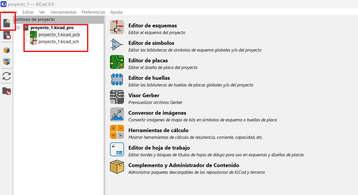
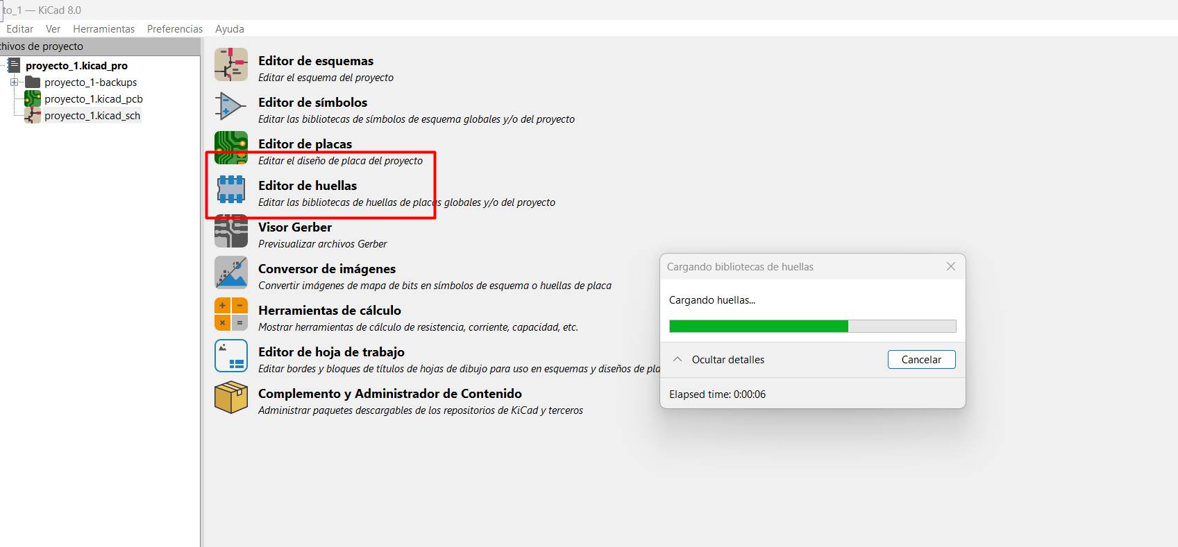
To start a new design, you must first create a new project. When you open KiCad,
the Project window will open. Click File → New Project, navigate to the desired location and assign a name to your project,
such as "starting". Be sure to check the "Create a new folder for the project" box, then click Save. This will create your
project files in a new subfolder with the same name you have chosen for your project.
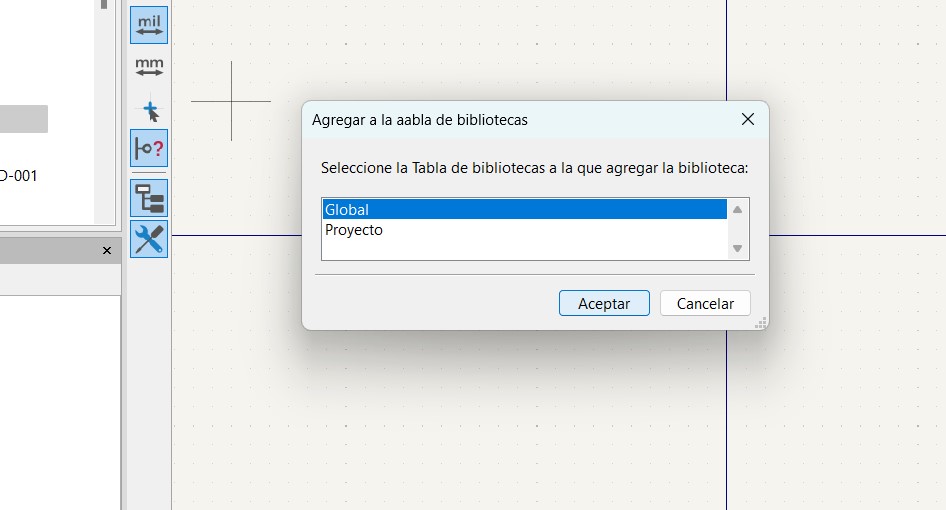
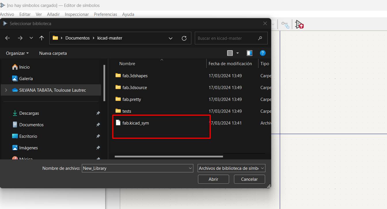
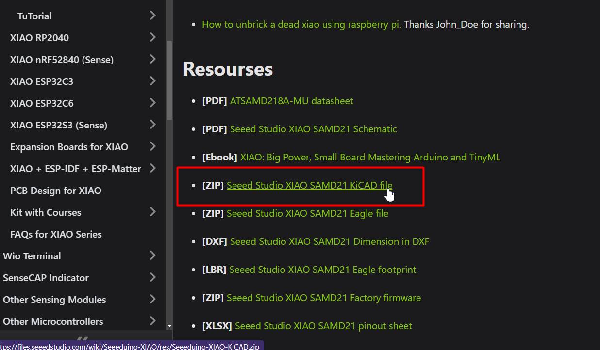
Download and place library
When you download the Fab Lab library to access the component symbols used in Fab Academy, you need to integrate it into KiCad so that you can access those symbols when designing your boards. Here's how to do it:
- Download the Fab Lab library from their github or wherever it is available.
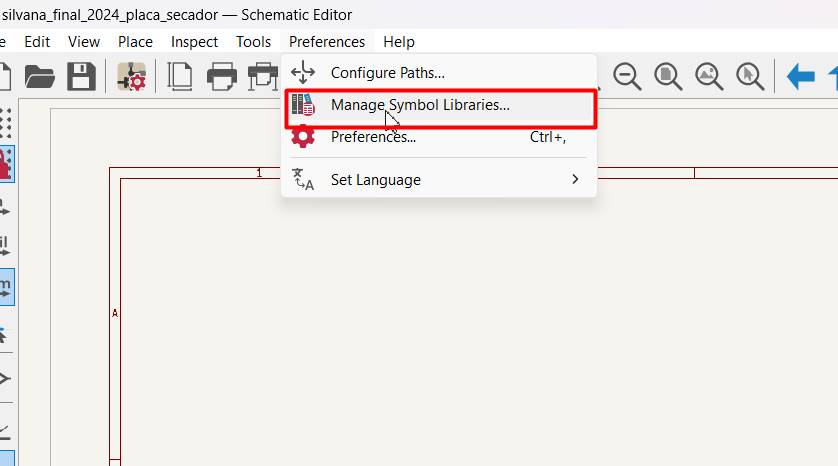
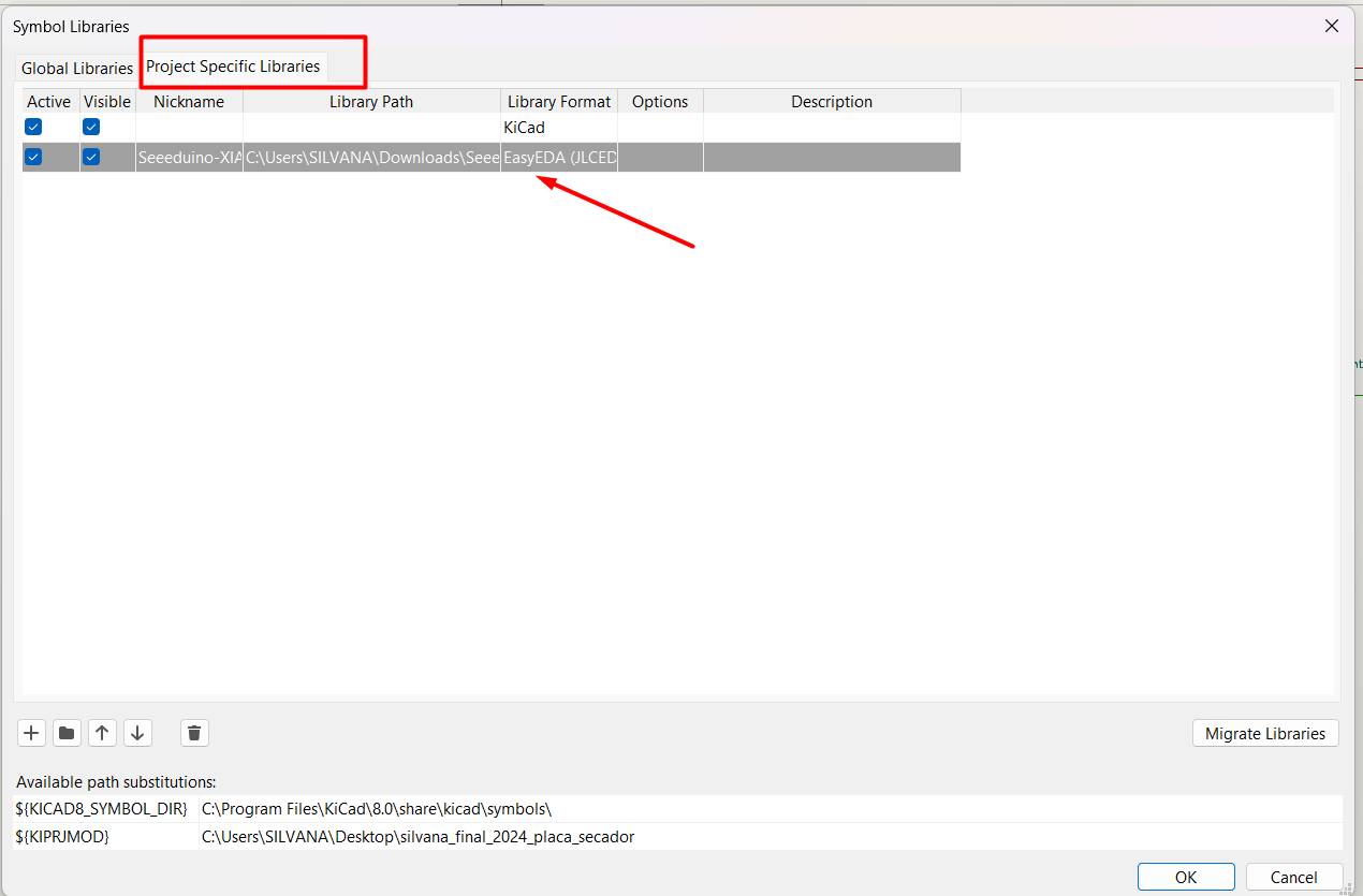
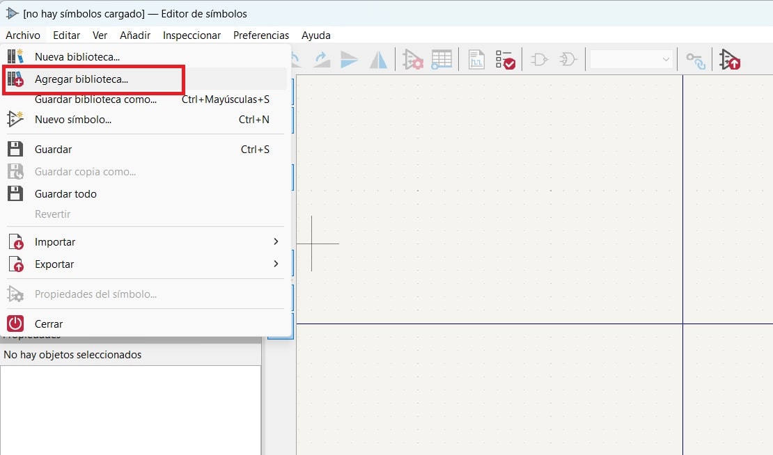
- Open KiCad and go to the symbol settings. You can do this by going to Preferences → Symbol settings.
- In the Symbol settings window, there is an option to add a new symbol library. Click the "Add" or "Browse" button and select the location where you have saved the Fab Lab library you downloaded, it may be zipped so you must unzip it in order to add it.
- After selecting the location of the library, KiCad should locate it and display the component symbols in its internal library.
Placing the components
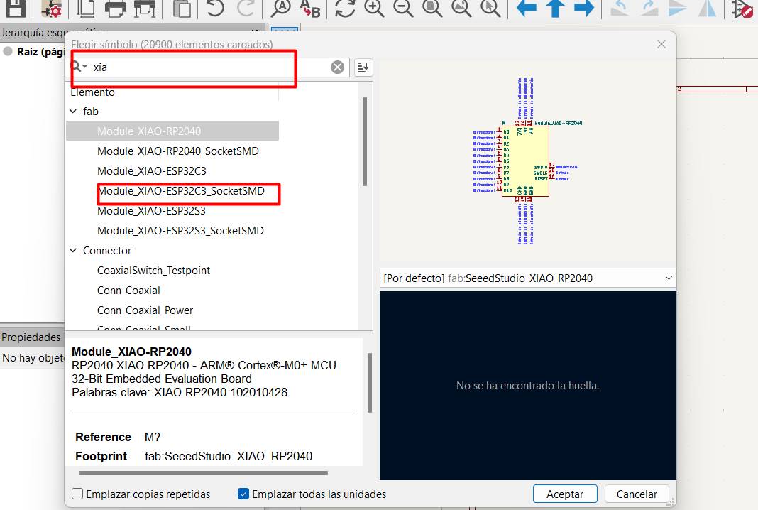
Since we already added the FabLAb library, we are going to look for our components, first the xiao, in my case it is XiaoEsp32C3
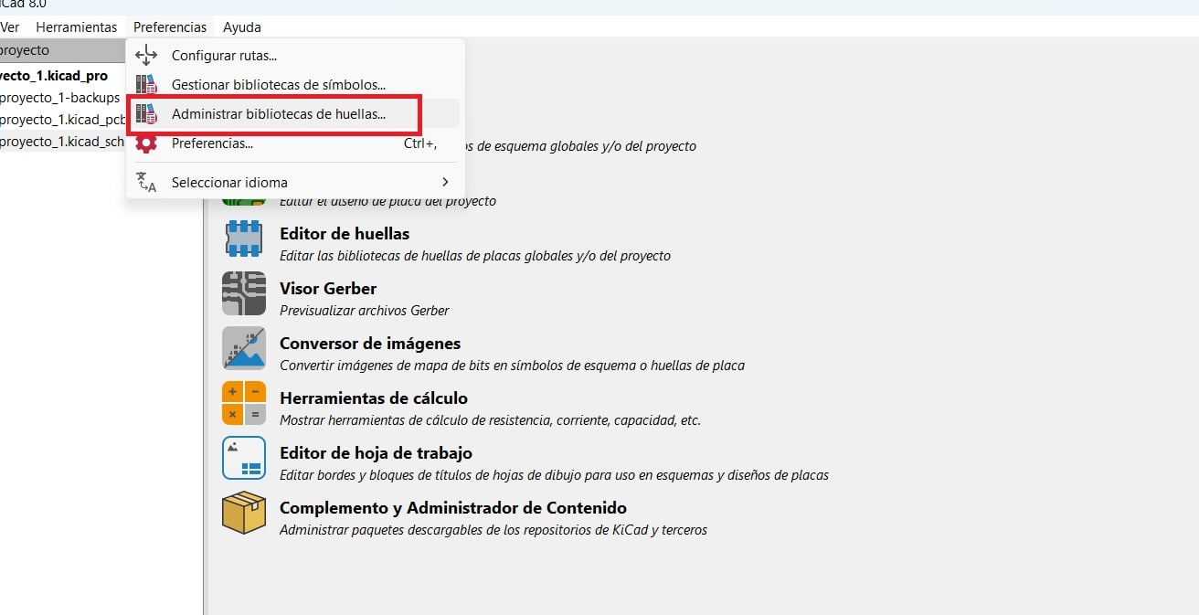
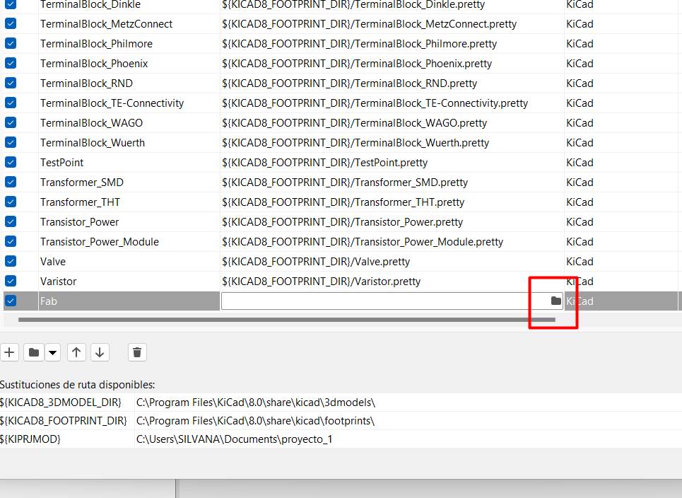
Now we realize that the symbology does not appear, so we are going to add it in manage fingerprint libraries
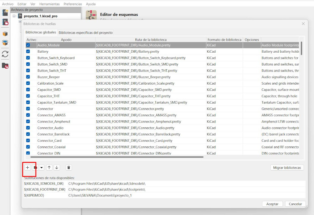
We click on this + symbol to be able to add a new module and be able to place the library, you have to close it so that it can load the tracks.

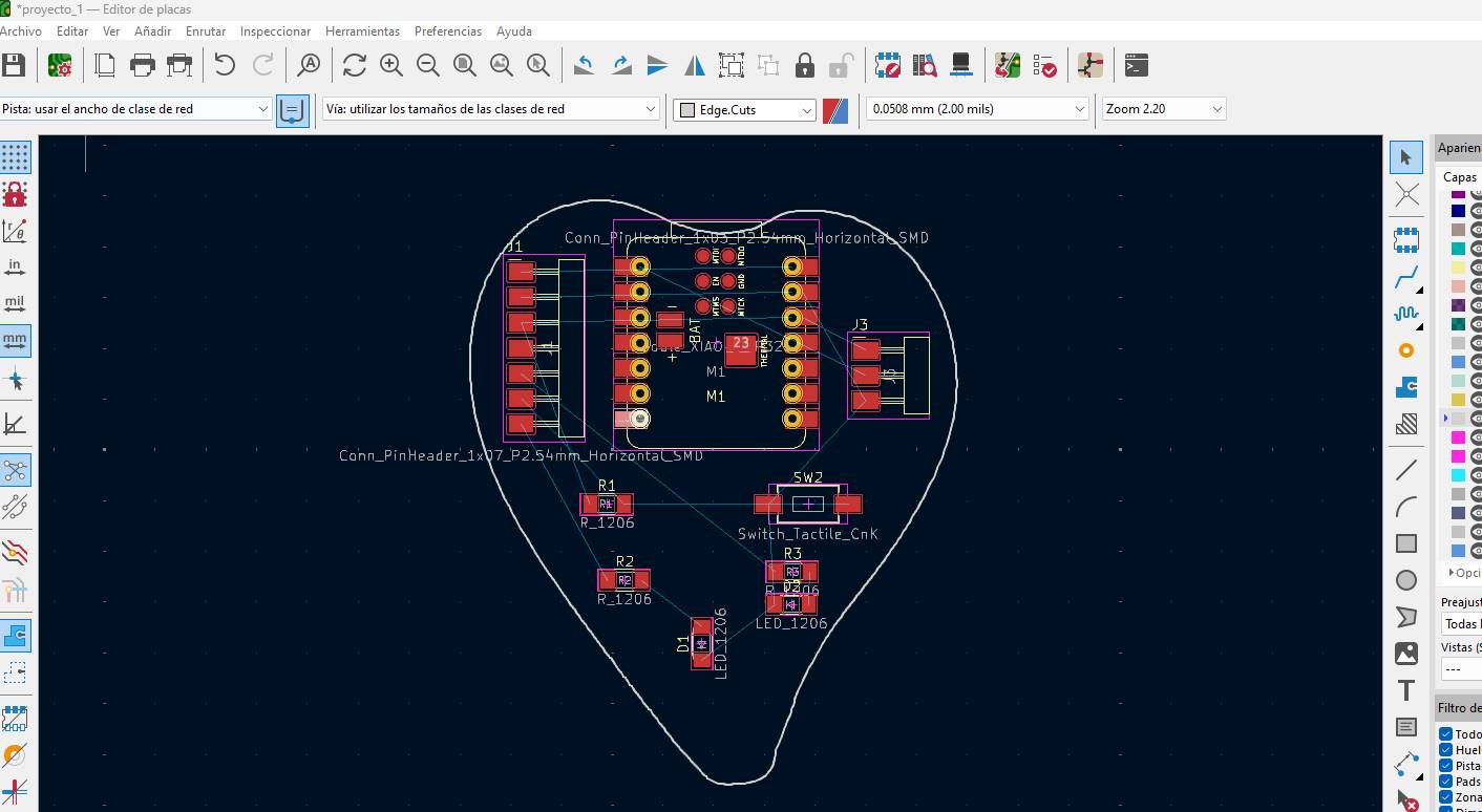
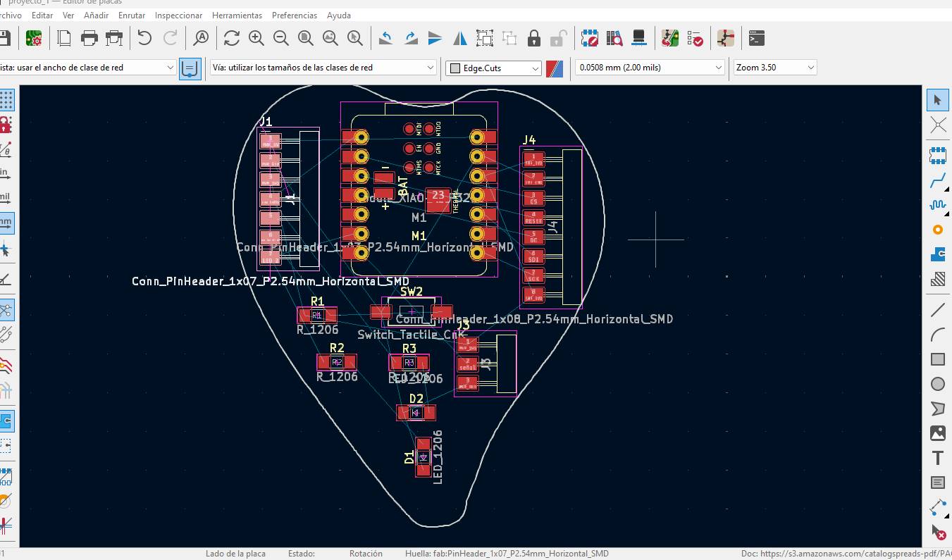
View of the three designs that were tested

Placing my pins, it actually needs 7
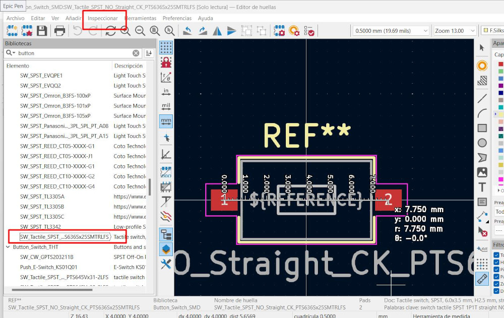
Inspect the measurement of the button
It was already looking better

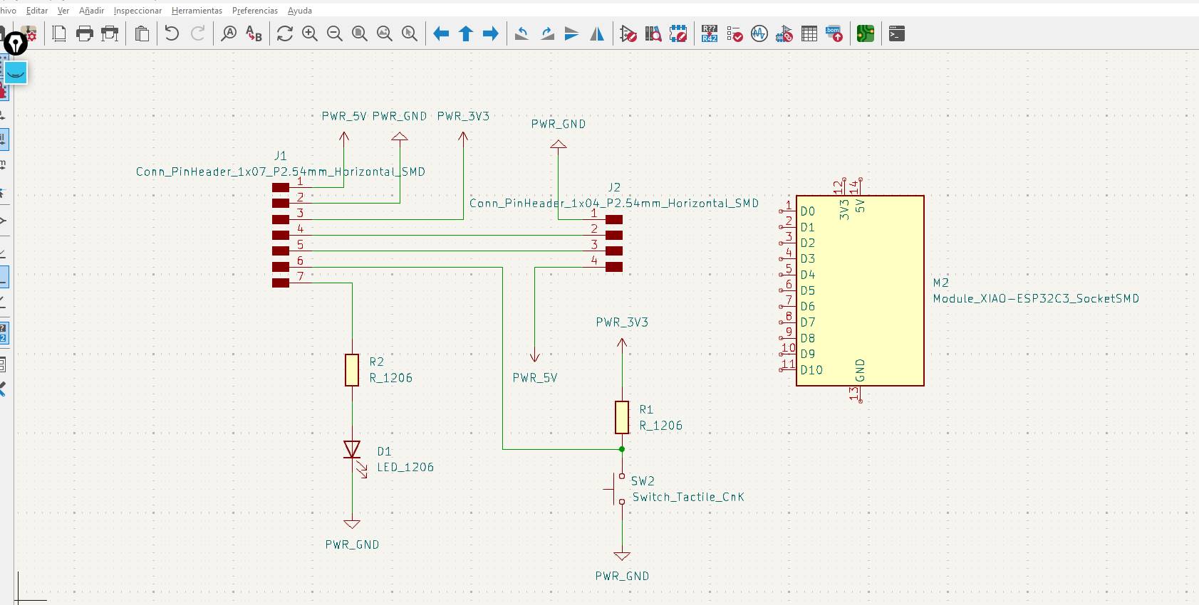
Here updating the schematic
I tell you that here I made a diagram for screen input