Description of the equipment
In our laboratory we have the following implements:
1. Mastek multimeter with test points
+ Info2. A Miniware DS213 oscilloscope.
+ Info3. A Logic Analyzer LA104
+ Info4. GW-INSTEK adjustable DC voltage supply with power cable and test points.
+ Info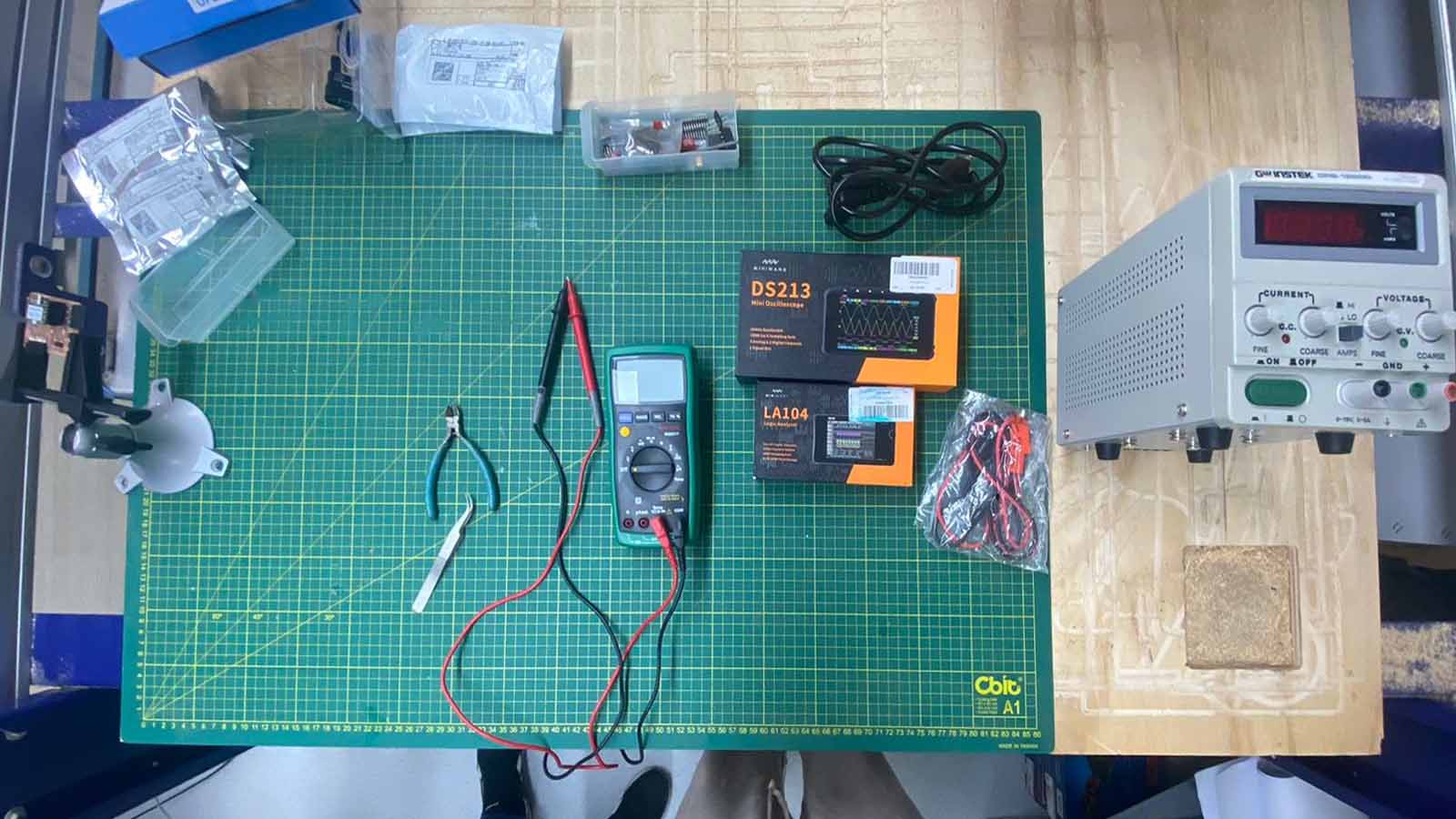
Test
Testing the Multimeter
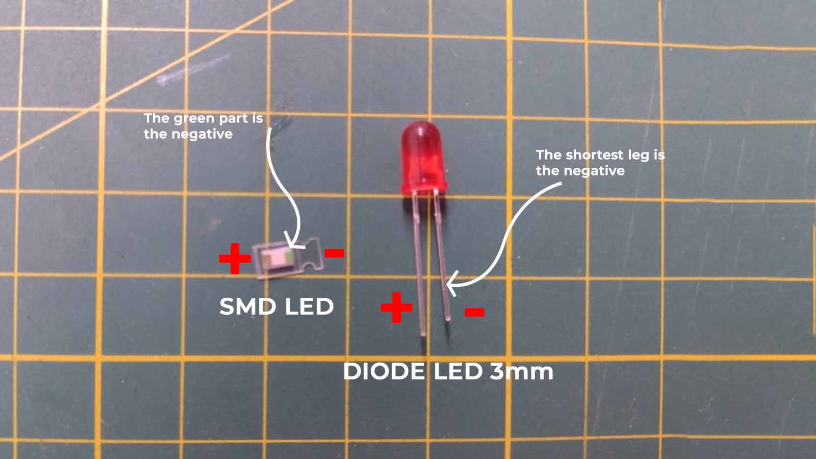
LED'S
For testing with the multimeter, we use as test object two LEDs, the first 3mm DIODE type and the second SMD LED.
Here are some pictures and the procedure with the multimeter to test the operation of the LEDS.
It is necessary to indicate that the negative node goes with the BLACK cable, while in positive with the RED cable, the same ones must be connected to the multimeter, verifying that the black cable is to the RIGHT and the black one to the LEFT side.
The result is that the LED type DIODE lights up without any problem, that is to say that our test 1 with the multimeter is CORRECT.
We tested the other LED ignition test, this time with the SMD, here is the result:
Everything is working properly! Two successful tests.
SMD RESISTORS
We test resistors, 499ohm and 1000ohm, for this case we set the multimeter by positioning the dial upwards pointing to the Ω symbol.
Consider that not always the resistance or its value will be represented on the multimeter, often it is important that it is one or two decimal places less.
Ω = Ohms
kΩ = Kilohms
MΩ = Mega ohms
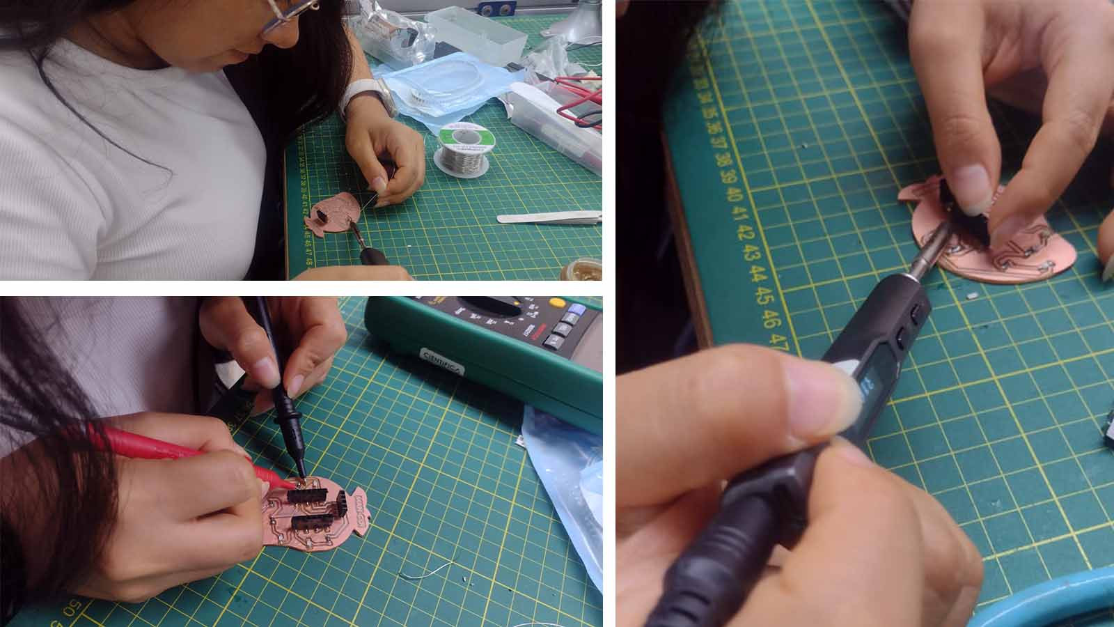
CONTINUITY
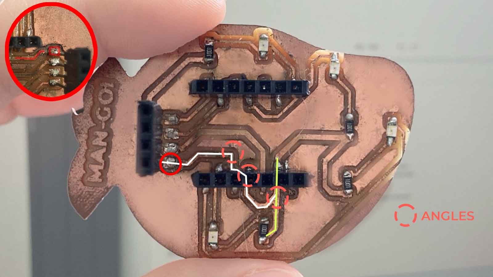
About continuity, from here we test with our Quentorres, fixing a point of the milled copper channel and another on the soldering of one of the pins of our board, the multimeter should make a sound when finding continuity, I leave evidence of the case
All correct with the tracks and their continuity, the plate does not short-circuit.
Testing the Logic Analyzer
A logic analyzer is an instrument to capture, display and measure multiple electronic signals simultaneously in a digital circuit, they are able to show the relationship and timing between many different signals in a digital system, it is the best tool for debugging digital circuits and digital communication systems.
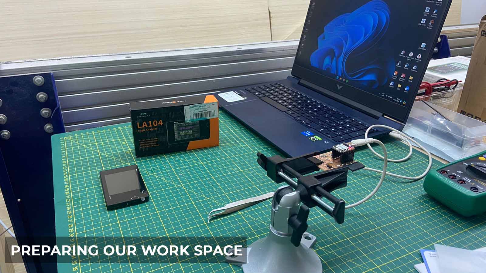
We did not have much experience using a Logic Analyzer, we understood that it is an electronic signal measurement device, I share this tutorial to understand it quickly:
Tutorial!With this information we have more clear what to measure, here are some parts of the Analyzer that is important to show to know the operation system:
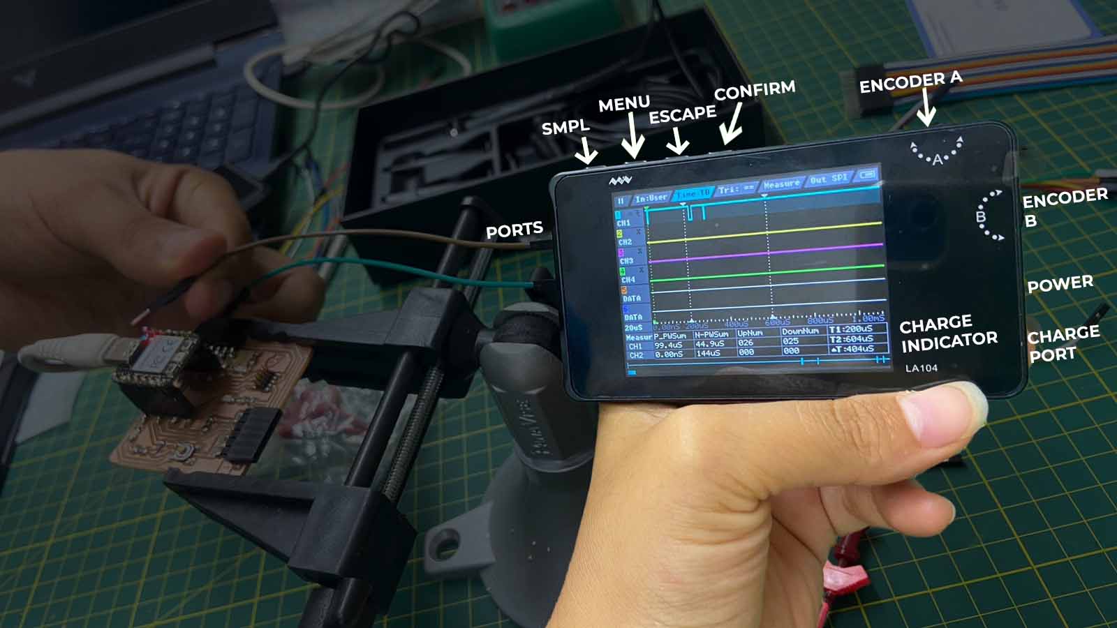
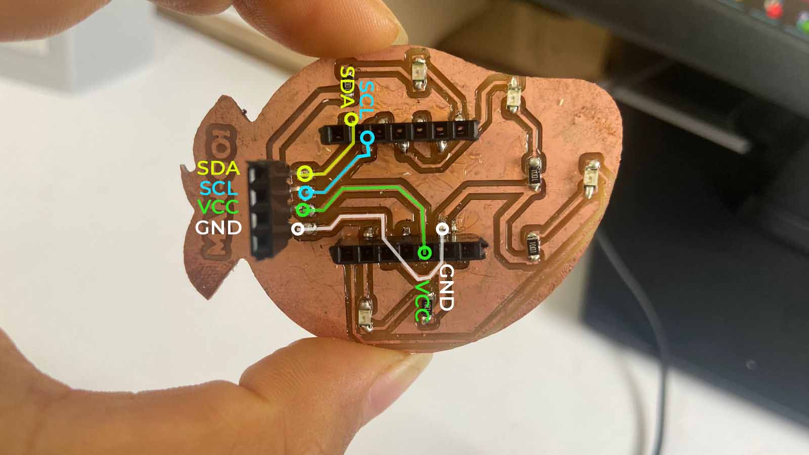
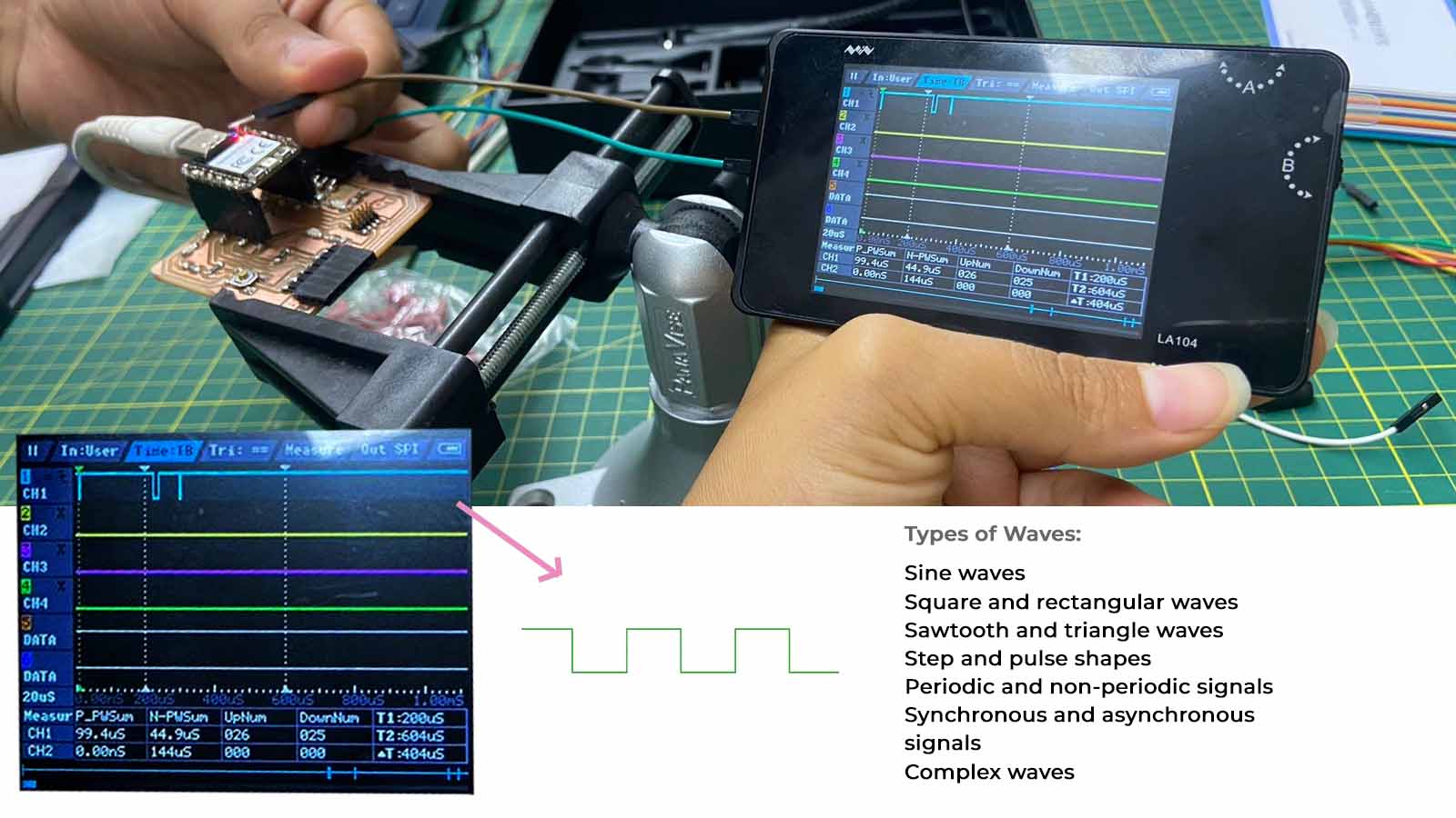
Knowing this, we can start connecting the ports with a jumper cable, we connect the GND (ground) of the Analyzer to the output of the corresponding Quentorres and the cable for CH1 (channel 1) with the free port to touch parts of our board, the intention is to verify the voltage and P_PWSum values with reference to the performance of the Xiao and its connection on the board.
Testing the Oscilloscope
It is an electronic measuring instrument for displaying electrical signals in a given time. These signals are expressed in graphs in which an electron beam passes through a coordinate axis on a phosphor screen.

From here, we decide:
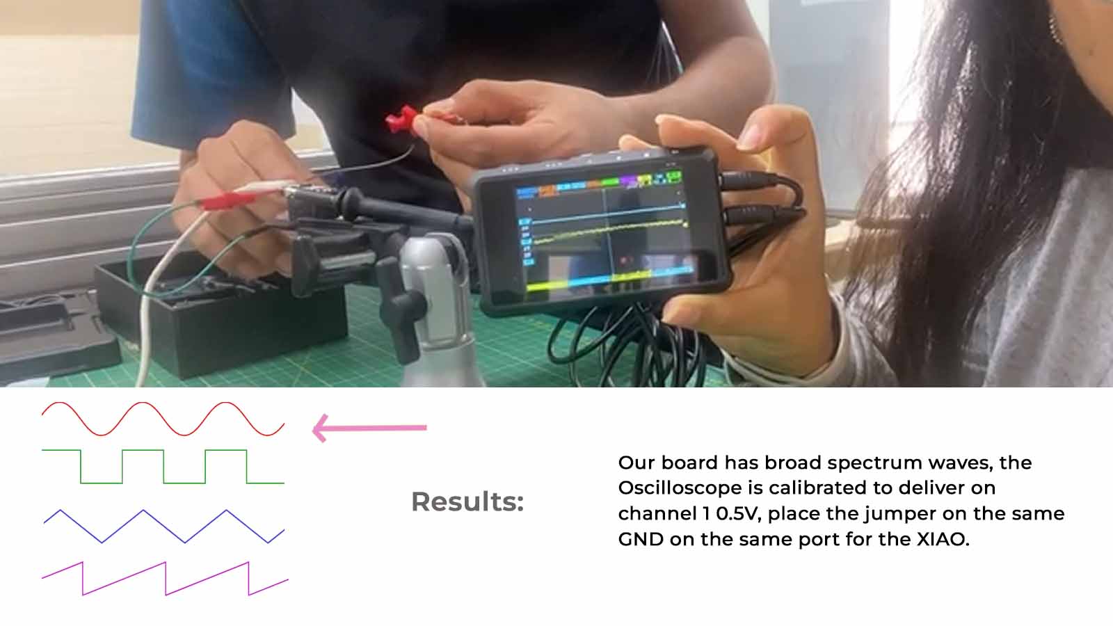
Place the diode to find the voltage of a channel, we set the voltage sending signal to 0.5V for channel 1, so that, using the swords, attached to the jumper applied on the XIAO and connected on channel 1 to the Osilloscope, we discover that there is conunication between these components.
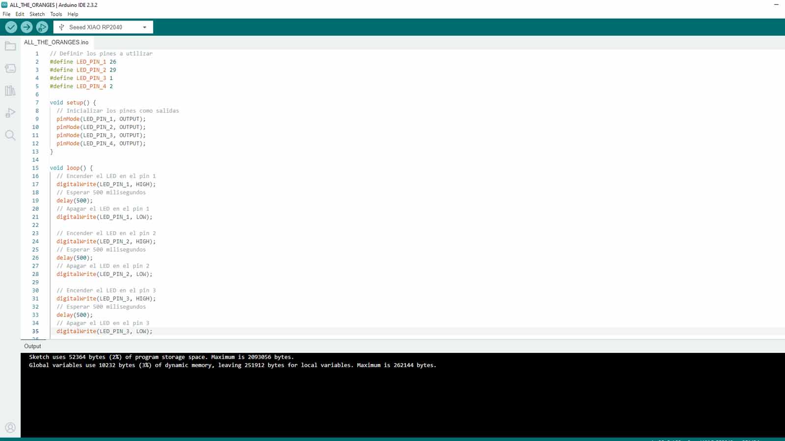
We had the result of a square wave, which means that it is a regular interval voltage, such as signals from TV, radio and other devices that use timing signals, this is due to the use of the LED blink programmed on the board.
Testing the DC Voltage Supply
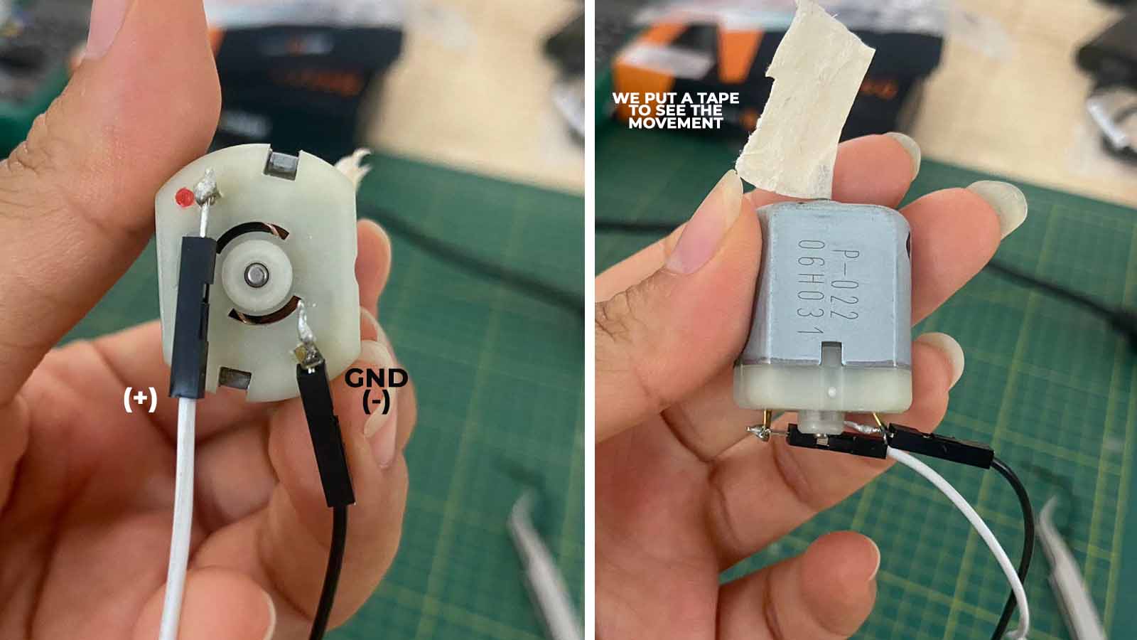
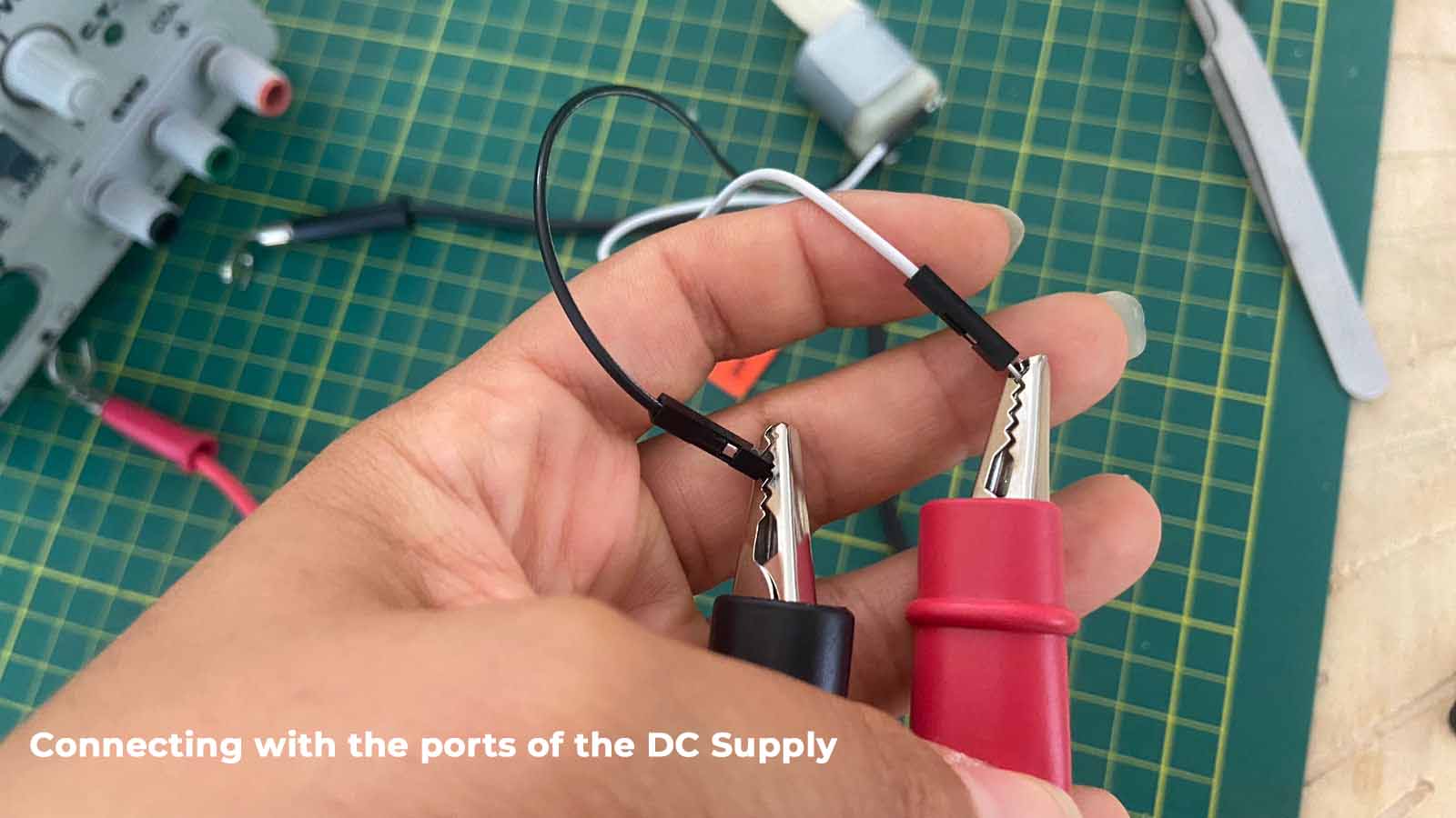
The tests with the DC Voltage Supply, we did them connecting the source with the two hook pins, in the photo is identified which are, so, using a DC motor with the soldering of their sources to two jumper, we connect the hook pins with the corresponding (black wire is ground, red wire is voltage) we started first with the ignition and were manipulating the voltage rise knob little by little.
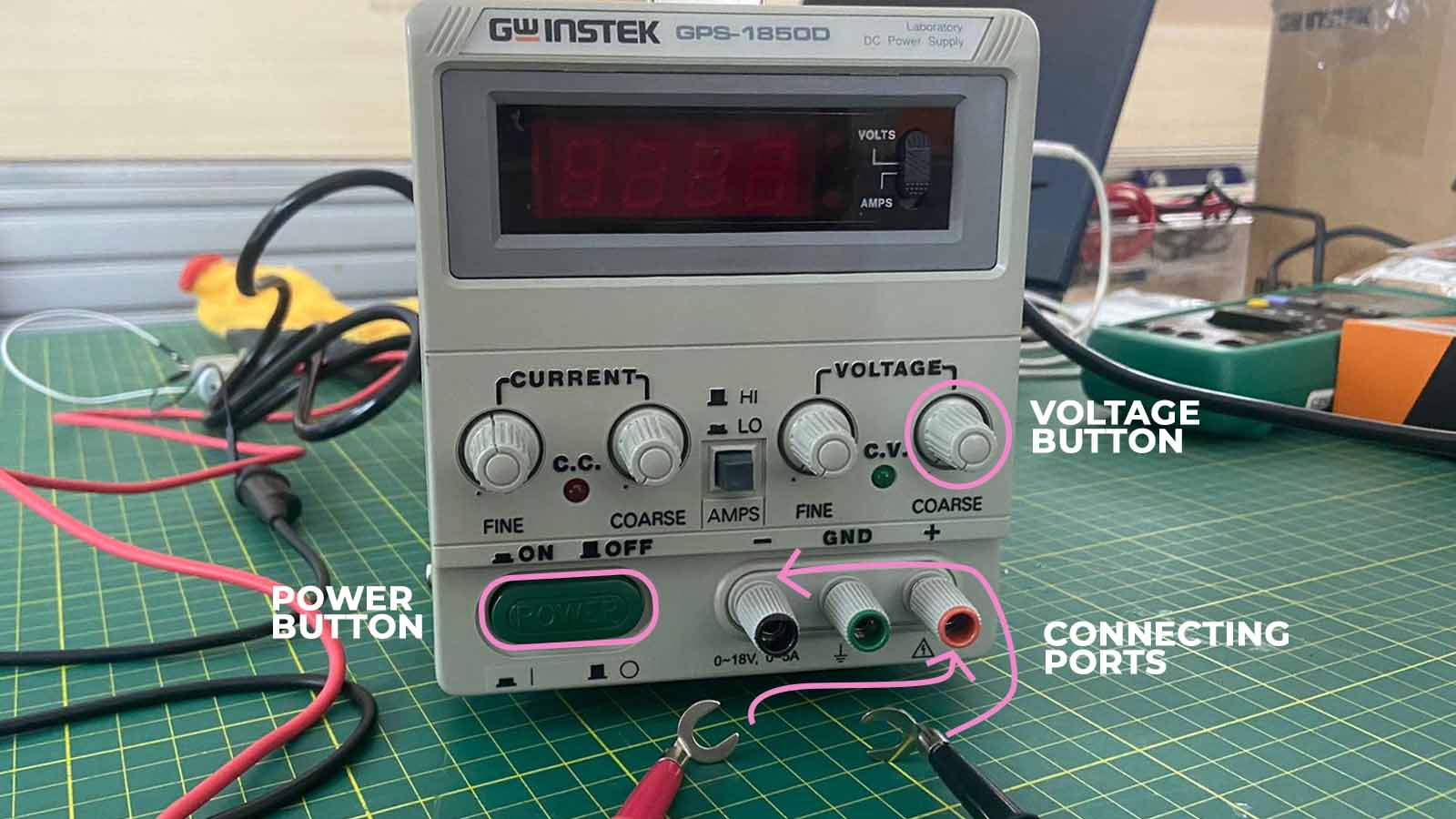
After identifying the basic operating buttons of the power supply, we proceed to the soldering of the DC motor with the male jumper wires.
After the soldering is done, we connect the male side with the source clamp wires.
From here we are ready to see the result.