Fab Academy
Arthur DEFRAIN

Week 4 
​Electronics Production

Goal

​Group assignment:
​​Characterize the design rules for your in-house PCB production process: document feeds, speeds, plunge rate, depth of cut (traces and outline) and tooling.
document your work (in a group or individually)
Document your work to the group work page and reflect on your individual page what you learned

Individual assignments:
​​Make an in-circuit programmer that includes a microcontroller by milling and stuffing the PCB, test it to verify that it works.

​Learning outcomes

​Described the process of milling, stuffing, de-bugging and programming
Demonstrate correct workflows and identify areas for improvement if required

Sample Headline

​Linked to the group assignment page
Documented how you made (mill, stuff, solder) the board
Documented that your board is functional
Explained any problems and how you fixed them
Included a ‘hero shot’ of your board

​ Find the right setting to cut a PCB   

In this part we will try to find the setting to cut propely a PCB with a CNC. I will use Fusion 360 to designe the PCB like in the previous week. Its a challenge i take to use as much as i can Fusion 360 to force myself to learn avery aspect of this software.
For the CNC i will use a Snapmaker 2.0, its a smaller CNC that th CanCam i use during week 7 so it will be more acurate, specialy on small details.

​Créer le fichier

I need first to creat a file in fusion to send to the machine, I will take the sample i just shaw previosly. its a test to find the smallest path you can have for your PCB, and also find the right setting for the cut. 

After i send it to the Manufacturing page, like in week 7, the only difference will be the size of what i cut, and the cutting bits. 

Here we will use PCB V-Bit, its a common and cheap way to machine PCB, the bit avec a very thiny point of 0.1mm.
The bit will plung in the PCB borad and remove a very fine layer of copper to creat the path we design.

We will machine this plate, it's a plate of baquelite with a fine layer of copper on it,
The Gaol is to remove just the copper, to keep the structural property of the plate.

Like in the previous week, we will creat some toolpath for this, but Fusion 360 don't a PCB path, so I will try different one

I will start tu use the 2D contour, it's use to removed the out of object, like the copper path.
Using the V-Bit and not a End-Mill like it should.

The first relust is not good, we don't have any path where we should have, its not the path but the setting of the bit.

The V-Bit Setting

Here is the setting of the bit, the dimension of it.

The part where we can change some setting is the the feedrate and the speed of the bit.
by default it was at 5000 rpm, so i change it to match the max of the snapmaker. and i also reduce the feedrate ( the quantity of material per revolve of the bit) i change from 15 in/min to 9 .
It will be longer but better.

I aloso change the depth of the cut from 0.1 mm to 0.02 mm depth.

The second test is betterbut still not good enought, the cutting look like too deep,

I retry with a better hight adjustement, and the resulte look good, the only concerne i have is in the very thin test part, all the copper is gone so i neet to oversize the path in my design to balance that.

With that result try to make the actual PCB, and im very happy with the first result.

Some part are good some not, specially when the path are stick one to the other, that creat short cut in the circuit.

​Et maintenant, faites le circuit imprimé, ou du moins essayez d'en faire un

With those good result, i redesign and adapte my CAD of the PCB to fit the property of the Snapmaker.
But i keep the same parameter form the test. I let the week end pass and monday we will have a lot of PCB to solder.
It was my mindset maonday morning but, i got the malediction from the PCB God. I cannot make an other good PCB.

So i start to look arrond WHY my Snapmaker decide to give up and dont make an other PCB .
But i dont look only the machine i look every aspect, like in the 5M method tool.

This tool is used to find where come from the problem or the issue, is composed by 5 different groups. This tool is used in the industry. For exemple, you buld a car, and it didn't start when you turn the key, can be cause by the material, the cable is faulty. Can be the Medium ( or environment) you try to start the car under water. Can be the machine, the CNC that buld the engin is no precise. Can be the methode, you try to start but the car run out of gaz ( or battery ). And finaly can be the workforce, they switch two wire. It often not only one cause that conduct to the problem.

​Ce que je trouve

​Le premier problème que je constate est que le matériau est plié et pas seulement un peu.

There is a difference of 1mm betwin the edge and the center, And because i clamp it the center stay to hight compare to the edge. I could take on who was not bend by chance to make the PCB.

The second problem is the accuracy of the Machine

The Bed of the Snapmaker it very wobly, you can move it just with the presure of you finger. so when you want to be very precise, like when we machine PCB with circuit path size comparable to an human air, you should not have this kind of mouvement.
I think is the nomber one factor of the randomness of the result. the calibration can be very difficult.

​Oui, je sais qu'il s'agit du format Smartphone et non du format paysage, désolé.

Solution #1 

Change the CNC

I will try on an other small CNC, a HANDIBOT CNC

Or use a cheapest one like the 1310 CNC Router

But after few test I still have the same problem, one time the PCB came well but just after with the same setting, the PCB came not good.
I pass few week testitng different PCB and property of the PCB design, like size of the circuit, stock to leave etc.
 
But at one moment i look the V-bit when its turning and I saw that.

I find out that the V bit is not all the time center, just a thiny bit, but we work at 0.1 mm here so even the smallest miss alignment can have a big impact on the PCB

But Why ?? 

I use  standard V bit that you can find on amazon or other online market.
but those have a small shaft lenght.
I try to use one with a longer shaft, to have a better fit in the spindle holder.

And it's good, the bit is in the right position.

After that i can make a complex PCB, like this one for the Week 11 for an ESP 32. And its double sided !!

​How to prepare the file

​After designing a circuit as in the week ​8 ​on Fusion 360. We're going to export it to Flat Cam, a software program specially designed for printing circuits. 

​Step #1 Create the files

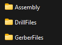
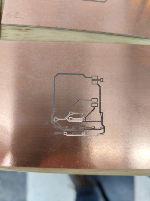
​After exporting and saving this file, we can see several categories:-The assembly file (we won't use it here)-The Drill file, for drilling through connections-the Gerberfiles file, several files with the tracks we need to create

​Step #2 Create the G-Code

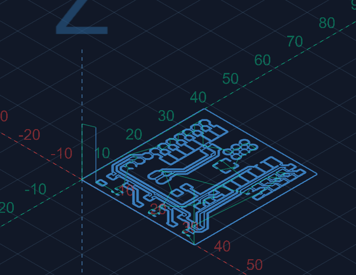
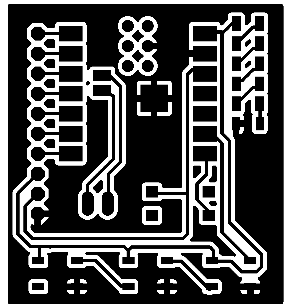
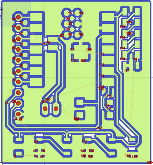
​Once on FlatCam, we can open two files: the first is the tracks we need to create, which can be found in Files > Open > Open Gerber, where we'll use "copper_top.gbr" to find the file created by merging; the second is the percages, which is optional. Files > Open > Open Excellon This time, we're going to search for the file in the drill document, where we can see the track (green) and the percages (red). 

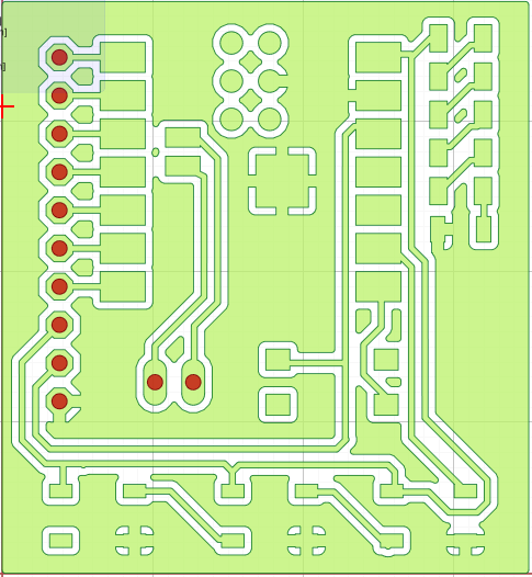
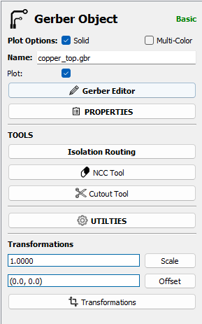
​After selecting the profile, I'll use the isolation tool. This tool will separate the tracks into individual circuits.

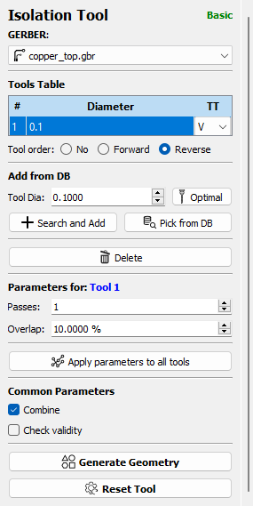
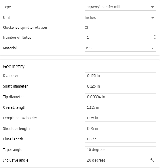
​In this section, we can define cutting parameters such as the tool size, here 0.1mm. the number of passes, i.e. how many perimeters around the tracks the tool will have to make to separate the tracks. and the overlap, i.e. what percentage the pass will pass over the previous pass.

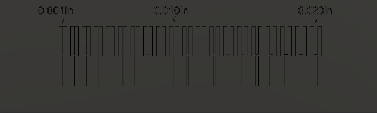
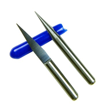
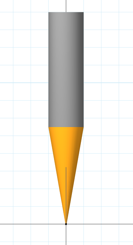
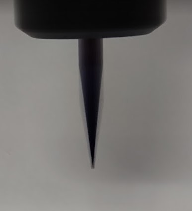
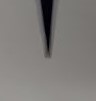
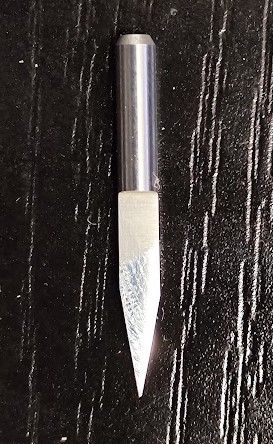
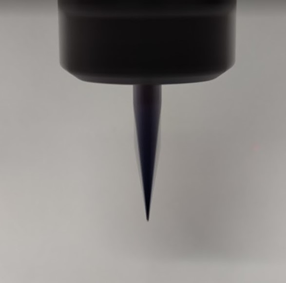
​You can also choose the profile of the tool, if it's a V mill or an end mill with a certain number of flutes (cutting part) C#

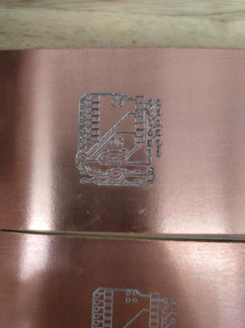
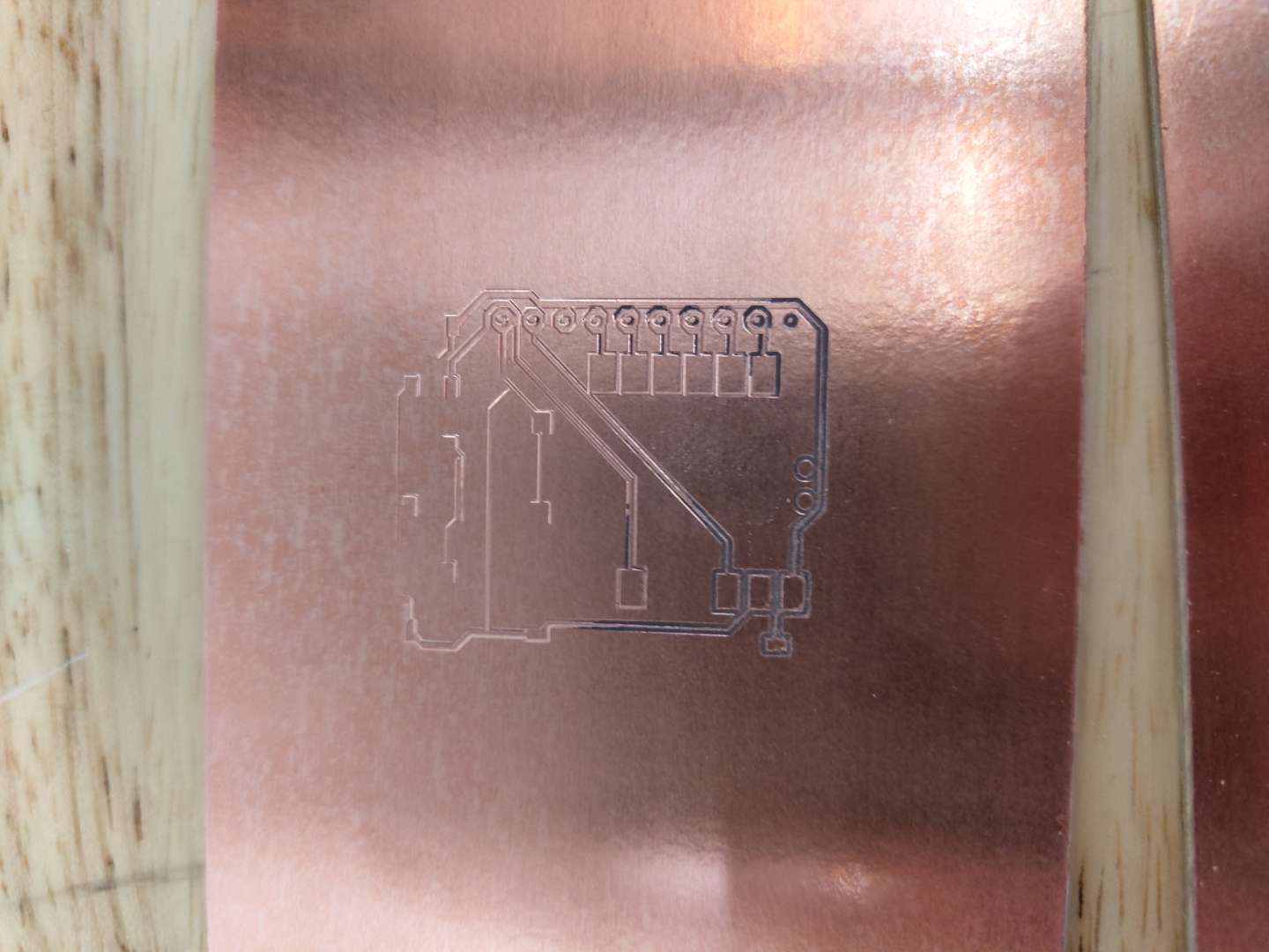
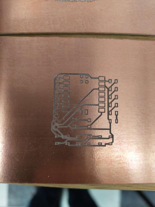
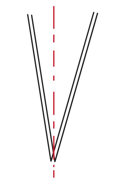
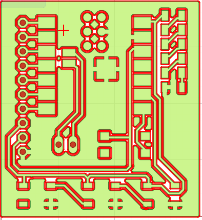
​Once the parameters have been chosen, we can validate and the software calculates the tool path. This is the red track, a flat path from the center of the tool.

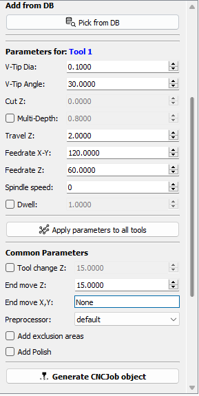
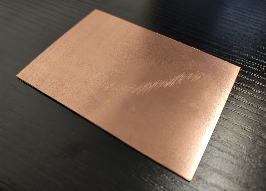
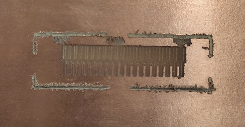
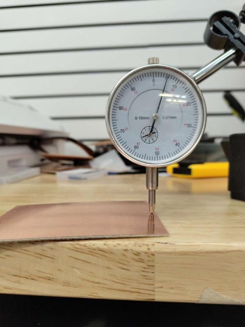
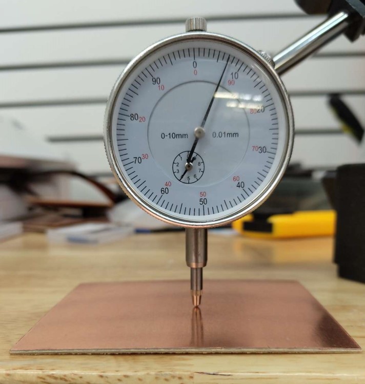
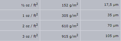
​Once done, we need to finalize and convert to g-code. To do this, we need to give the tool profile a dimension. This depends on the blank PCB. There are several thicknesses of copper layer, expressed in oz/ft2. Thanks to conversion tables, you can find out how much thickness you need to remove to create the track. In my case, I have 2oz/ft2, which gives me 0.07mm of copper to remove. To be sure, I'm going to remove 0.2mm, to counter possible level differences (plate not perfectly flat). CNC

​After this step, the profile turns blue, meaning that the Gcode is ready for export.

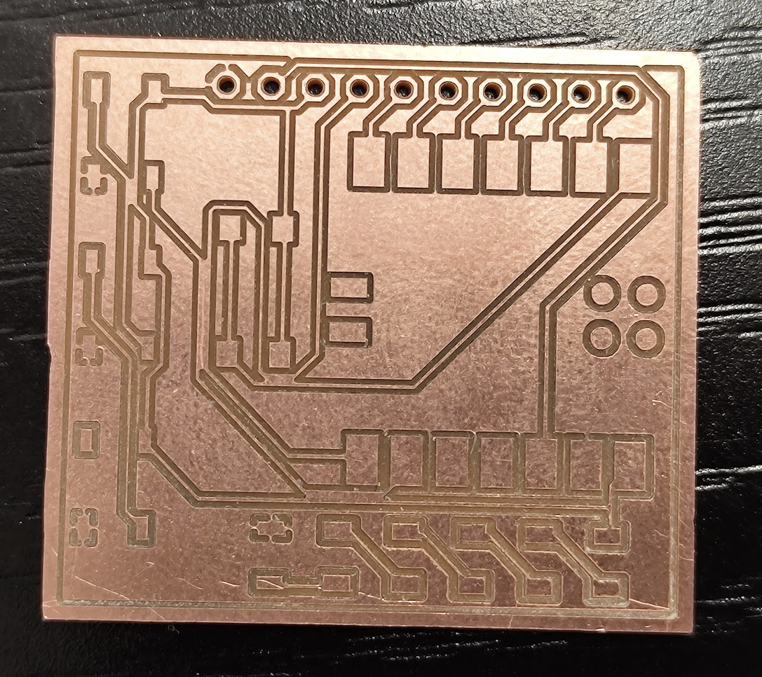
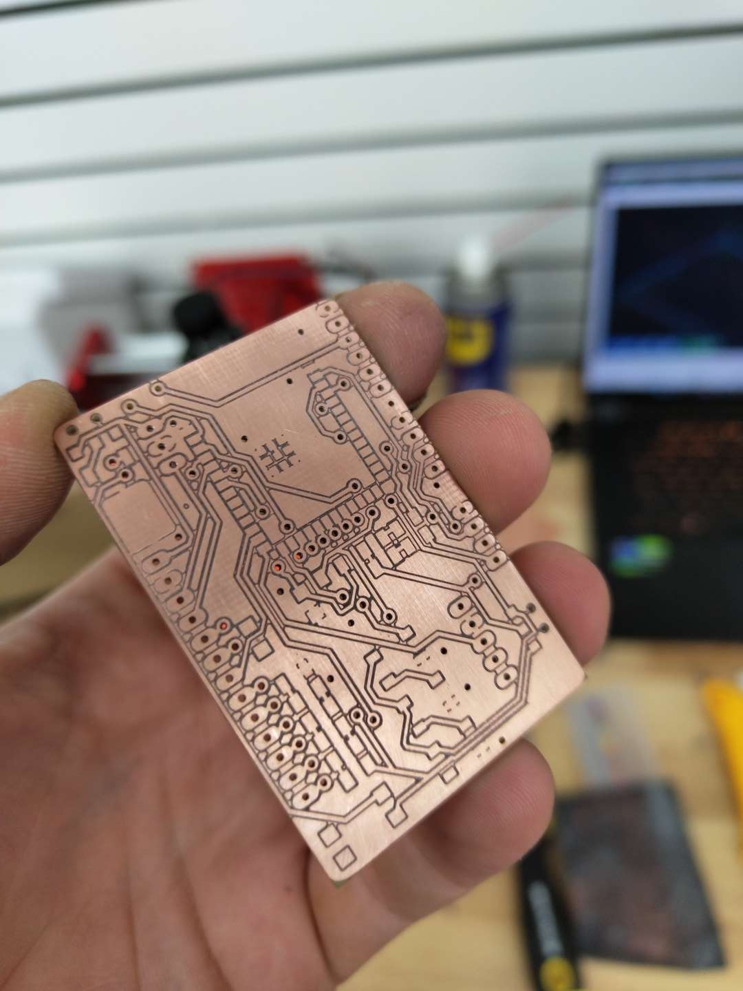
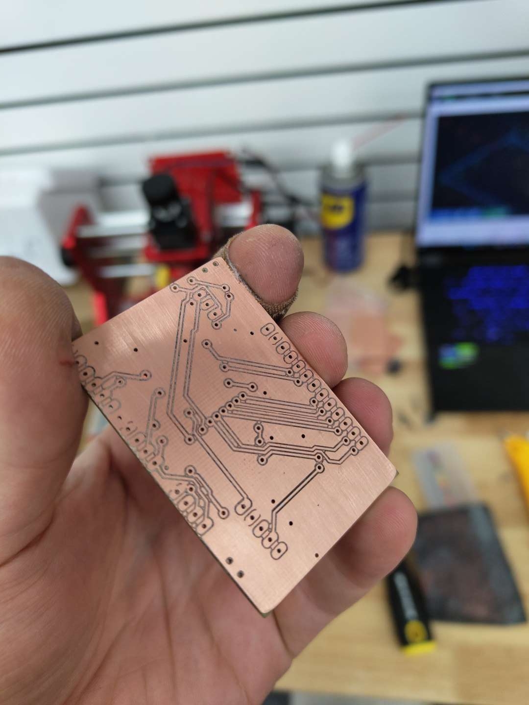
​Step #3 Making the PCB

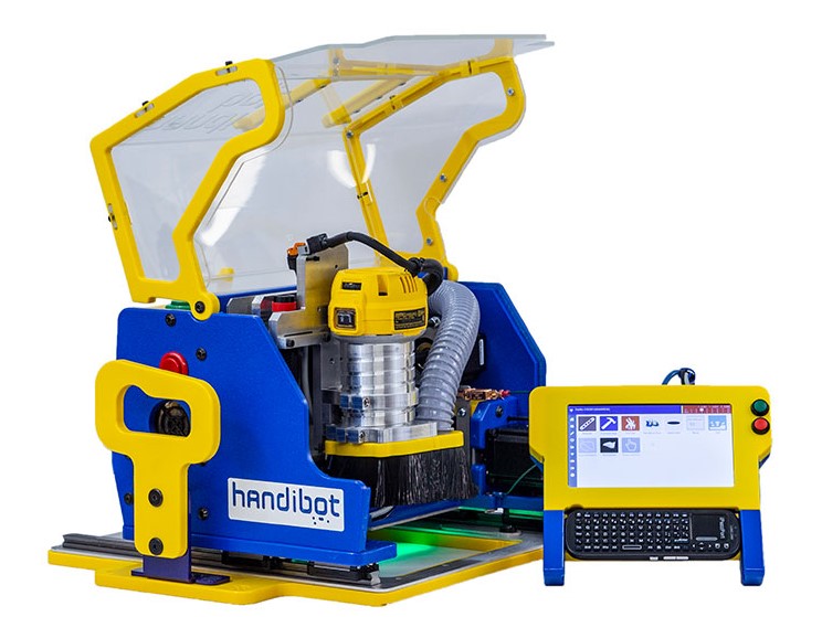
​Once we have the G-code, we can open the Gsender application, a CNC control software. All we have to do is open the Gcode and follow the steps as in Cnc week.