Fab Academy
Arthur DEFRAIN

Week 8 
​​Electronics Design

Goal

​Group assignment:
​Use the test equipment in your lab to observe the operation of a microcontroller circuit board (in minimum, check operating voltage on the board with multimeter or voltmeter and use oscilloscope to check noise of operating voltage and interpret a data signal)
Document your work to the group work page and reflect on your individual page what you learned

Individual assignments:
​​Redraw one of the echo hello-world boards or something equivalent, add (at least) a button and LED (with current-limiting resistor) or equivalent input and output, check the design rules, make it, test it. Optionally, simulate its operation.

​Learning outcomes

Select and use software for circuit board design
Demonstrate workflows used in circuit board design

Sample Headline

​Linked to the group assignment page
Documented what you have learned in electronics design
Explained problems and how you fixed them, if you make a board and it doesn't work; fix the board (with jumper wires etc) until it does work.
Included original design files (Eagle, KiCad, etc.)
Included a ‘hero shot’ of your board
Loaded a program and tested if your board works

​ Individual Assignment   

Here we will pass trought the process to design a PCB (Printed Circuit Board​). We will use Fusion 360, its a CAD software but also a ECAD ( Electronic Computing Aid Design ). It was call Eagle before but its fully inclued in Fusion 360 now

Re design The XIAO-RP2040

Your PCB will use a XIAO-RP2040 as development board, I can import from exixting library, but here for learning purpuse I make it from scratsh.

In the software an electronic composant is an assemble of 3 different files.

The Electronic Symbol: it will be use the make the electronic circuit, connect to other elements.


The Foot print: Its the representation of the connection for the soldering.


The 3D representation or Package: Its optionnal but in Fusion we have the chance to combine the electronic with the CAD design so we will use it.

Step #1 The Electronic Symbol 

The symbol it what we will use to create the connection abd our circuit.
to creat one we need first to creat a new componant. 

In Fusion 360 open the files and select new electronic library.

After we arrived in the library tool, it here that we will creat all the different componant of the XIAO-RP2040. the first step is to creat the symbol.

Here the goal is to represent the XIAO-RP2040, we can use the pinout picture or just look our board tocreat the shape and put the right number of pin.

The line tool is used to make the shape of our board, here its simple we need a square. we can also tune it with deferent line style and corner.

After the shape, the most important the Pins, its where we will make the connections. We need to represent every single connection of the board. In our case we need 14 pins on each side + 2 pins for Vin and GND ​underneath.

At the end we need to give name on our pin, take the pinout from the datesheet and put the same name, this way we dont get lost in the process.

Step #2 The Footprint 

The footprint is a copy of the layout of the physical connection, the golden part of the picture, to have the same on our PCB to have the soldering pad 

We find the same tool as before, like line and name tool, thay have the same purpose as before.

We find 2 new tools, they are use to add and place the soldering pads, select the left one if you use material than you can solder on top of the board (SMD), and le right one if the connector pass trought the board (PTH).

You can mesure or refer to a datasheet to have the proper spacing and dimension for the pads

Step #3 The package 

The package is  optional, we dont need it to make the PCB. But I will do it because I want to add it to my CAD files.

I will not draw everythink , I just download the 3D files and add it to the electronic files.


Here we will open a traditionnal CAD, and here we can add the files we just download and save it .

After all of that the last step is to connect the pin of the Symbole to the footprint.

After that we just need to save and our new element is complet 

View and Download online 

Design our PCB

The Goal here is to creat a PCB with at least 1 LED and 1 switch. We will creat a prototype PCB for the fina project.

Step #1 export the shape of our PCB

This step is optional, if you have place or if you want to have a square shape no need to use this one.
This step show how to export a sketch form a CAD to the PCB to have something that can fit in our design.

Here we just need to draw a sketch in our CAD design, with a little bit of space between the different pieces, this way everything can be assembe.

After finish the scketch, we will not make a extrusion like in the week 2 but we will use the tool "Create a PCB ". this way the shape will be use to creat our PCB. i use this Video to help me. 

Step #2 Creat the electronic schema

For the rest i look this Video to help me to design the PCB 

I start with a new electronic design, from there i can start placing my different element and link them.

From here we can add different element of what we need, resistance, switch etc ...
But we need be careful, the eement we will select impact the rest of the of the PCB design.
For exemple : a simple resistance, its always the same symbol (exept if you live in the NA).
A simple rectangle with two connector, one on each side. But for the footprint every resistance are different, depend of the size, the distance between the two connector, and the methode of fixation ( solder on the board or trought the board) so we need to be sure of wich one we select.

LED : WS2812B, adressable RGB LED.

Resistance : 130 Ω, Size 1206

Switch : Normaly Open (NO) switch

XAIO-RP2040 :the devellopement board we just creat before.

After adding al the defferents elements, i need to connect them like on the left, to do that i use the tools NET to creat wire between the elements to have the power and the data they need. I simply need to select one output and draw the line to the destination, if i need i can creat a branch, it represnt by the small round thing on the line , that mean the 3 or more line on that point are connected. 

When done i can save and push the design to the next step, the PCB document.

Step #3 Creat the PCB Document

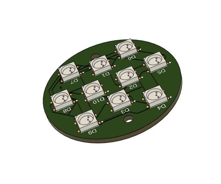
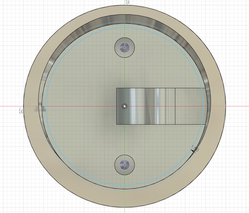
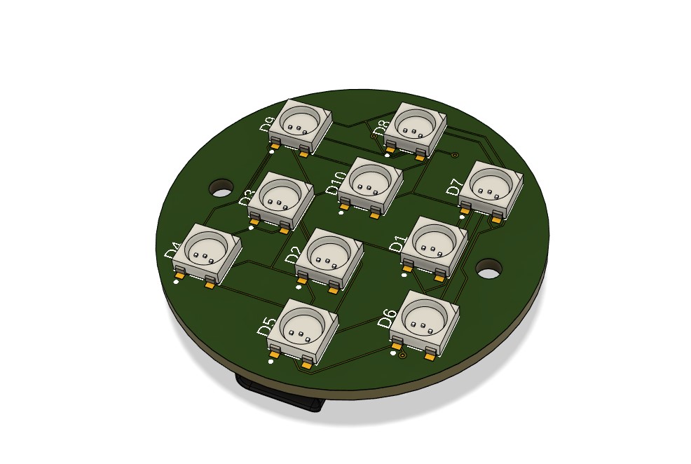
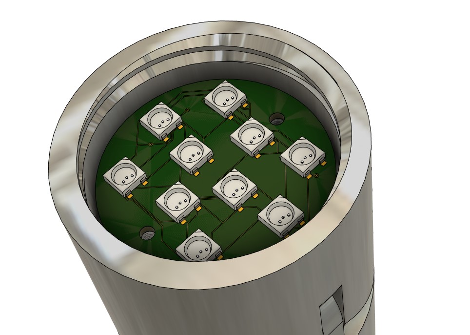
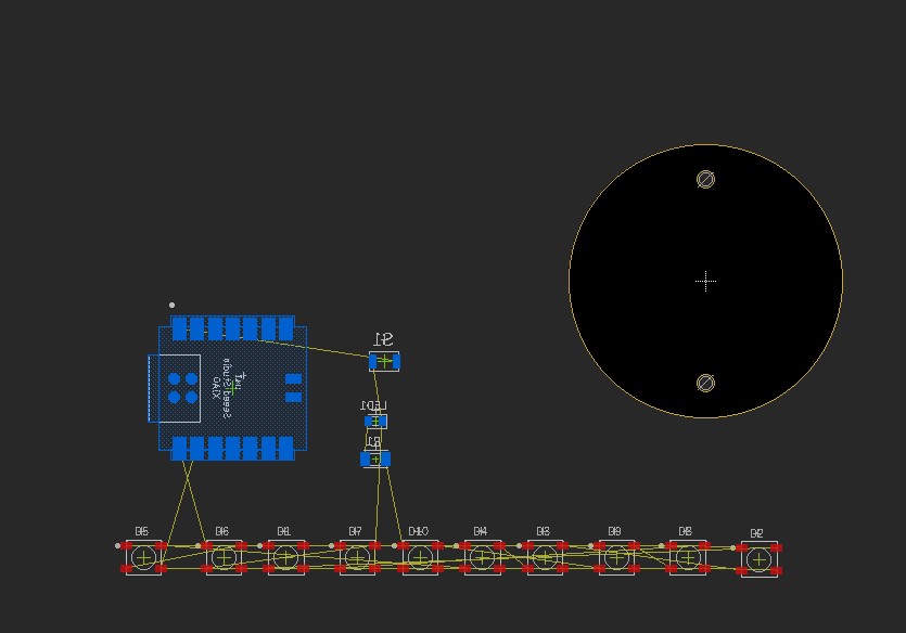
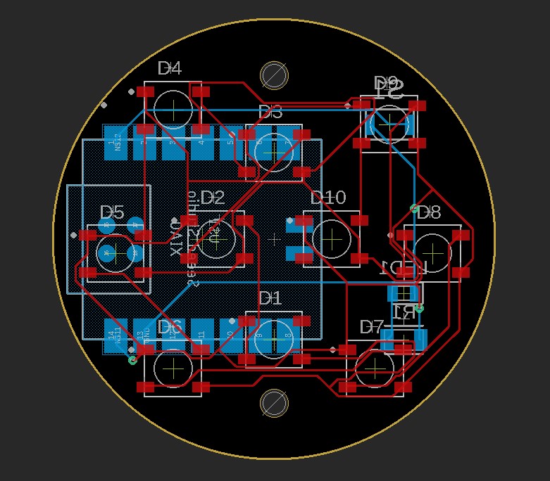
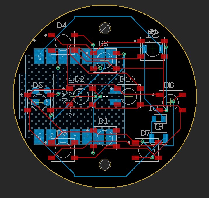
When you open the PCB document, you find this, the physical PCB, represent in black with the yellow line, by default is a square but if you follow the video i use in the step 1 to have a custom shape you should have this round shape.

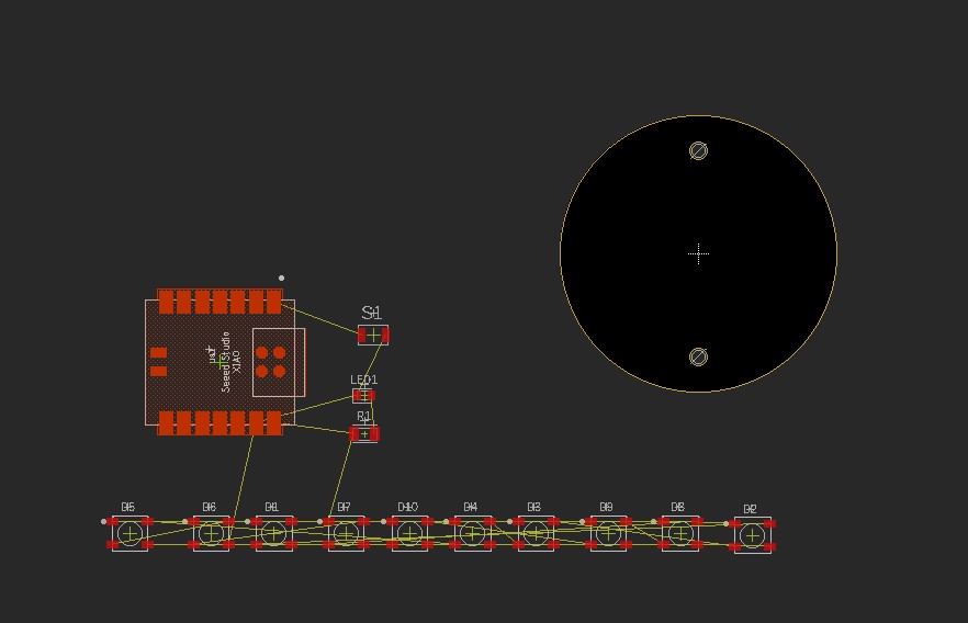
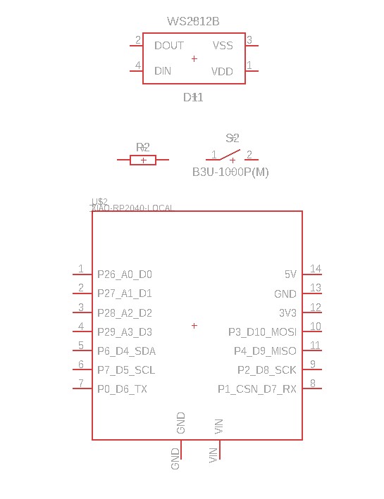
You can also see the different componsent of our circuit all in red and some line between them. 
The red means is on the top layer, can be blue for the bottom or other if you have mutiple layer PCB.
The line represent the connection between the different components, like the connection of the switch with the XIAO, the led with the resistor, etc. the goa here is to put everything in the black circle.

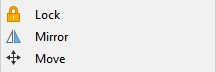
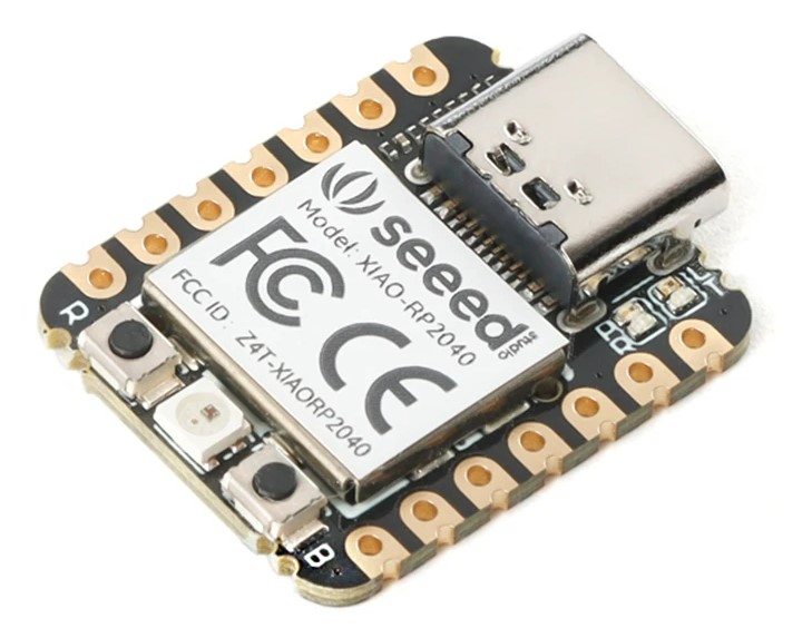
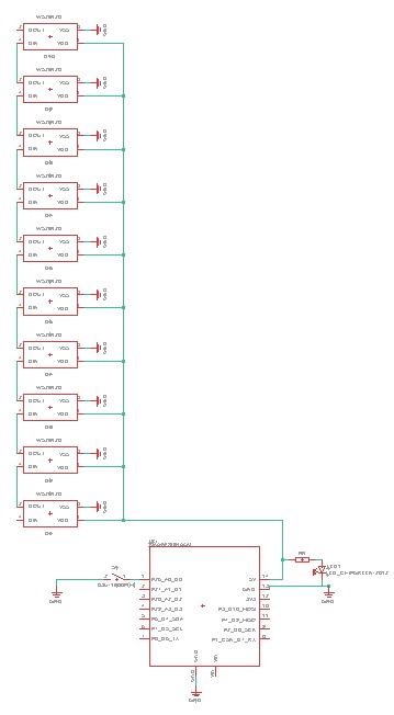
First we can pt our XIAO, the switch and the LED with the resistance on the bottom layer of the PCB, to do that we can use the mirror tool. That will flip the pieces and automaticly change the color in blue, that mean the softwar consider those device under the PCB.

And after we can place them on the board.

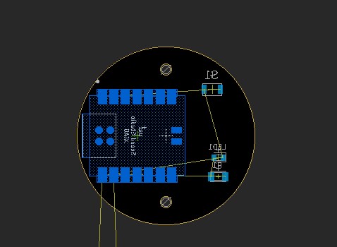
After that we can do the same for the rest of our RGB LED, to be a little bit more clear we can use that tool " Single layer view" to have only the top or the bottom view.

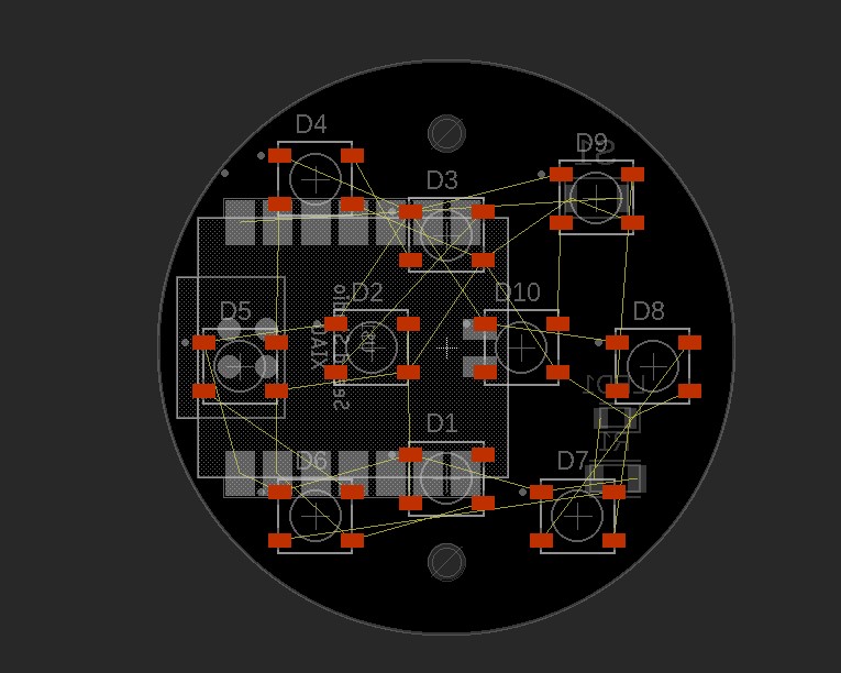
After that we can creat the route between our elements, we can do it manualy or let the software do it for us. It what we will do.

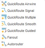
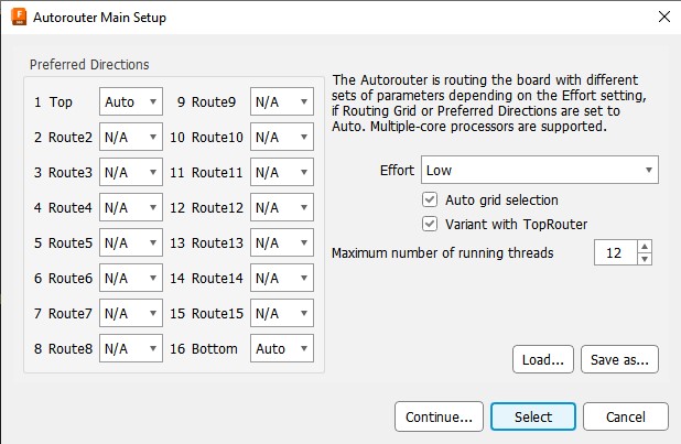
So We will use the Autorouter tool. we need to tell him where we need to creat path, here we let the top and bottom layer, when we will use and really make our PCB we should let only the top layer. after we have the effort setting, it how hard the software will compute to find a path.

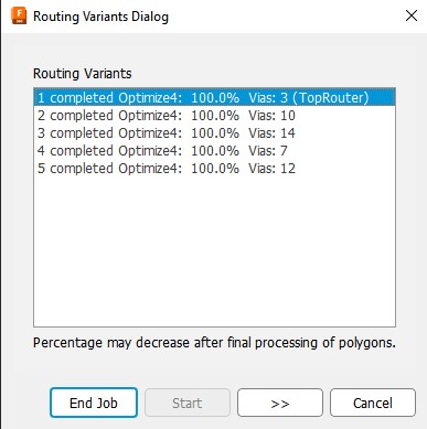
Find a path with 3 via 

​Find a path with 10 via

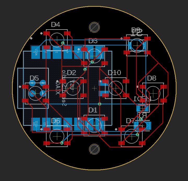
​Find a path with 14 via

​Find a path with 7 via

A Via is a path between the layers to pass from one to the other, less via mean less back and forth. I select the first one cause it have less via. After that i can save it and push to 3D PCB with this tool

Step #4 Creat the 3D PCB 

Here we don't have a lot to do, the software make nearby everthing for us. just with the tool we just used , the 3D files is creat with all the different composent. 

We just can save it like that and add him on different CAD design like other part .

Downlaod Xiao Files Here PCB​

​ Groupe Assignment   

​The Multimeter

​​A multimeter is a versatile electronic measuring instrument used to measure voltage, current and resistance. It can also often perform other types of measurements, such as capacitor capacity, circuit continuity and temperature. Here are the main features of a multimeter:

​In short, the multimeter is an essential tool for technicians, engineers and do-it-yourselfers to diagnose and solve problems in various electrical and electronic devices.

​How do I use it?

​Here's how to use a multimeter in a concise way:

1. Set up the multimeter: Select the type of measurement (voltage, current, resistance) with the rotary selector.
2. Connect leads: Connect the black lead to the COM terminal and the red lead to the appropriate terminal for your measurement.
3. Take the measurement: Apply the probes to the points on the circuit where you want to measure. Read the result on the display.
4. Interpret the results: Check that the values displayed correspond to expectations or safety specifications.