This week I will take the first steps in designing my own PCB board. I am looking forward to this!
to learn / to do
Group assignment:
- Use the test equipment in your lab to observe the operation of a microcontroller circuit board (in minimum, check operating voltage on the board with multimeter or voltmeter and use oscilloscope to check noise of operating voltage and interpret a data signal)
- Document your work to the group work page and reflect on your individual page what you learned
Individual assignment:
- Redraw one of the echo hello-world boards or something equivalent, add (at least) a button and LED (with current-limiting resistor) or equivalent input and output, check the design rules, make it, test it. Optionally, simulate its operation.
looking ahead
what I already know
What I know about electronics is what I learned in the recent weeks.
what I want to learn
I really want to learn what goes where on a board, and especially why. Also, the role of all the components, like resistors, capacitators and generally how these things work. I know that there is current, and volt and watt, and I know they have a relationship with each other, but I do not exactly know how. I really want to understand this.
electronics
The week started with an excellent introduction of electronics by Erwin. He walked us through the basics, which was very enlightening for me. Here are some concepts that I picked up from it.
Electrons
Electrons are what an electric current is made up of. Electrons moving from + to - generate an electric current.
Voltage, V, Volt
The voltage is the potential difference in a circuit. The eagerness by which the electrons want to move from + to -. This is determined by the difference in potential between + and - . The analogy that Erwin used for this is a high waterfall with a big distance between top and bottom. But you can also think of this as a watertank:
 source:https://learn.sparkfun.com/tutorials/voltage-current-resistance-and-ohms-law
The pressure at the end of the hose below the tank, where the arrow is, can represent the Voltage.
Current, I, Ampere
The current is the amount of flowing electrons. Using the watertank analogy, when the water starts actually flowing out of the hose, this flow rate is the current. With a narrow hose, this flow rate or current will be less than with a wider hose. If we want the flow to be the same through both the narrow and the wide hose, we will have to increase the amount of water in the tank with the narrow hose.
 source:https://learn.sparkfun.com/tutorials/voltage-current-resistance-and-ohms-law
Resistance, Ω, Ohm
Which brings us to resistance. In this analogy, the resistance is the width of the hose. A narrow hose gives higher resistance than a wider hose. A circuit with a higher resistance will allow less current to flow through it. With a narrow hose, it takes longer before the tank gets empty. With resistance in the form of a resistor, a battery will discharge slower. When you connect the two poles of a battery without a resistor, it will discharge immediately, resulting in a short circuit. If you add a resistor in the circuit, you slow down the discharge.
Ohm’s Law
The relationship between Voltage, Current and Resistance is represented by Ohm’s Law:
V = I * R
If you take a look at the image below, and state that
- the narrow hose has a resistance of 2Ω
- the wide hose has a resistance of 1Ω
- the tank has a pressure (voltage) of 1V
Then you can determine the current for the narrow hose as follows:
1V = I * 2Ω
I = 1V / 2Ω
I = 0.5A
And for the wide hose as follows:
1V = I * 1Ω
I = 1V / 1Ω
I = 1A
 source:https://learn.sparkfun.com/tutorials/voltage-current-resistance-and-ohms-law
Power, P, Watts
Power is the rate at which energy is transferred. It is described with the relation between Voltage and Current, see this formula:
P = V * I
Using the watertank analogy, say you add a waterwheel under the end of the hose and let the water flow on to it. The wheel under the wider hose will be able to generate more power:
P = 1V * 1A
P = 1W
The wheel under the narrow hose will generate less power:
P = 1V * 0.5A
P = 0.5W
Resistor, R, Ω
A resistor is a (passive) component that functions as a barrier for electrons, it limits the current. They have no polarity, meaning that their orientation tp PWR and GND does not matter. They come in different values expressed in Ω (ohm) like 10Ω, 100Ω, 680Ω, 1000Ω (1KΩ) etc. There is also a 0Ω resistor, that you just use as a bridge. There are also resistors with variable values, for example a potentiometer.
Capacitor, C, farad
A capacitor is a (passive) component that functions as a storage tank for electrons. It fills it up when the current flows and at the other side emits a steady flow of electrons. You can use it to remove noise or spikes from the current. Take for example a speaker. When you turn a speaker on you will typically hear a little pop, unless you add a capacitor in the circuit. Capacitors also have different values, expressed in F (farad). One farad is a lot of capacitance, the capacitors we work with are more in the range of uF (microfarad) or nF (nanoFarad)
LED/Diode
A diode lets electrons through in only one direction. A special kind of diode is the LED, a light emitting diode. Diodes have polarity, they have a positive (anode) and negative (cathode) side. A diode needs a little bit of “pressure” to “open”. This is called the forward voltage or Vf. The Vf of a LED is listed in its datasheet.
For example, on my Hello World board, I want to use a blue LED. The Vf of a blue LED is 3.2V, which means the LED will need at least 3.2V to work.
Let’s assume that my board will be powered by 5V. This is too much for the LED to work with, so I will add a resistor that will drop the voltage to 3.2V. That means that this resistor has to drop 5-3.2 = 1.8V . The LED also requires 20mA to operate. With these two values I can now calculate the value of the resistor I need: 1.8V / 0.02A = 90Ω .
I select 100Ω , because that is the nearest higher value that we have.
Transistor, Q
With a transistor, a small current can amplify a bigger current: use a small current, or a small voltage, to open a large current. This bigger current can be from the same source, but also a different source.
An example is the nametag board that Erwin designed. It has something like 25 LED’s, and these are too much for the microcontroller to handle. So what the controller does is controlling the transistors, and these transistors will open a bigger current that is directly drawn from the battery.
Microcontroller
The microcontroller is the brain of the PCB. It is an integrated circuit, a circuit in itself, much like the circuits that we are building with the PCB’s. But much,much smaller. It is different than a microprocessor , which is more or less a calculator with some memory. A microprocessor is more versatile, and has also digital and analog inputs and outputs and digital interfaces for communication.
Group assignment
Use the test equipment in your lab to observe the operation of a microcontroller circuit board (in minimum, check operating voltage on the board with multimeter or voltmeter and use oscilloscope to check noise of operating voltage and interpret a data signal)
Below are some photo’s of the group assignment. We worked with the multimeter, measuring voltage and trying to predict the voltage that will be measured.
 Paola measures the voltage between the voltage regulator that Erwin made and battery. This is 8.7V, close to the 9V of the battery.
 Here Paola measures the voltage between the voltage regulator and the nametag board. Now it is close to 5V, meaning the voltage regulator drops the voltage with 4V. I forgot the correct name of this converter, but I believe it is a voltage regulator to fix the faulty capacitors that were on the board.
 Playing around with LED, trying to make the LED light up. In this photo the wiring is correct (red on the anode, black on the cathode) but the light is not on. Maybe because the LED is too big for the multimeter.
 Lighting up a tiny SMD LED
Individual assignment
Redraw one of the echo hello-world boards or something equivalent, add (at least) a button and LED (with current-limiting resistor) or equivalent input and output, check the design rules, make it, test it. Optionally, simulate its operation.
KiCad
The program that we use to design the PCB boards is KiCad. It consists of different tools, but I only used the Schematic Editor and the PCB Editor.

Schematics Editor
With the Schematic Editor I define what components go on the board, and how they are connected. The components that I select are partly from the DigiKey library, but mostly from the Fab component library. I already downloaded and installed these libraries during bootcamp week.
Henk gave us a list of the components that we were supposed to use for this assignment:

Making a design in the Schematics Editor consists of the following steps.
- Adding the symbols for the components
- Generate symbol reference designators
- Add values for the symbols that need them (for example resistors and capacitators)
- Add footprints for the symbols that do not have one yet
- Connect the symbols
After the first step, the order does not really matter
You add a component by pressing A in the Schematics Editor. This will bring up a dialog window with a list of all the components that are known to KiCad. In the search bar you can type in a word to filter the list. I used the word “fab” for example to get a list of the that are in the FabAcademy inventory. When you click a component in the list, its symbol will be added to the sheet.
When I have all the components on my sheet, it is time to give them all their reference designator. This is just a letter in combination with a number. The letter tells me something about the component type: resistors get a R, capacitators get a C, headers get a J. microcontrollers get a U etc. The number is just a counter, so the first resistor becomes R1, the second becomes R2 etc. You can let Kicad generate these designators by selecting “Anotate Schematic…” in the Tools menu.
After this I can make the connections between the symbols. There are two ways of making connections in KiCad: by drawing lines between the symbols or by using labels. Which one you choose seems to be a matter of preference. I went a few times back and forth between the two. Below I show both versions. I settled for the one that uses mainly labels, and use lines only in smaller sections.

schematic design with lines

schematic design with labels
When all symbols are connected, I need to add values for the resistors and capacitator. I can do this by pressing E when the symbol is selected. This calls up the Properties Dialog of said symbol. Here I can change the value. I can also select the Footprint for this symbol.

The Footprint is a description of the physical component: sizes, shape etc. This Footprint will be used in the PCB editor, where I will layout the actual board.
You can see which footprints are still missing by selecting “Assign Footprints…” in the Tools menu. This brings up a dialog with all the components on the sheet and their selected footprints.
With all symbols connected, annotated, footprinted and valued, it is time to perform a “Electrical Rules Check”. You can do this by clicking on the little button in the top bar that looks like a checklist with a red checkmark.
Below is an example of the result of this error check. It shows errors in the dialog, and points with arrows on the sheet to show you where these errors are. In this case, I am missing a label UPDI and there is also a problem at pin 6 of the controller, which is not connected. That is no surprise, as I just deleted the UPDI label from the controller to show what this Error Dialog looks like.

After correcting the errors and a last visual check, I can switch to the PCB Editor to design he board itself.
A --> Add symbol
R --> Rotates the selected component
X --> flips the selected component
E --> symbol/label properties dialog
PCB Editor
The PCB Editor is where the physical board gets designed. That is why it is important to have the footprints for all the components, as these footprints specify things like size, shape and clearance for these components. The PCB editor is also where the traces will be routed that connect all the components. These traces are going to be milled by the tool, in my case the Modela CNC router that we have in the lab. It is important that KiCad knows about the limits of this tool. We determined these limits in the group assignment during Electronics Production week.
So the first step in the PCB Editor is to tell KiCad the limits (design rules) of the tool that I will be using to mill the board. The most important rule is defined by the diameter of the endmill-bit. This is 0.39mm, which means that the individual track on my board need to be at least 0.39mm apart. This is called Clearance. I define these parameters in the Board Setup Dialog (File –> Board Setup…)
In the images below, I changed the values for Minimum Track Width and Track Width and Clearance


Then I select “Update PCB from Schematic” in the Tools menu. This retrieves all the components and their connections from the Schematic that I designed earlier and places their footprints on the sheet without any structure at all. This is what they call a “Rats Nest” and it is up to me to convert this into a well layed out PCB design.

The idea is that you eliminate all the thin straight lines between the components, by adding tracks with the line editor. These tracks will end up on the physical PCB board to connect the components.
I struggled a while with this. In the beginning it was hard to understand what I actually was doing, and also what the graphical representations actually meant. I peeked a lot in other peoples documentation: Nadieh, Erwin from last year, and also my fellow student Ben . What really helped was using the 3D view of the board:

What also helped was when I started to trust the line editor. I was trying to control and guide it around the components to the best of my abilities, but found that when I just dragged in a straight line it would try to find its own way. Much easier!
I had not much trouble with the simple connections between for example the LED and the microcontroller. But creating GND and PWR lines was harder. It felt weird to have all the GND pads connected to each other, I somehow wanted to point them all individually to the central GND pad. Same for PWR. But by looking at examples from others I found that that was indeed not neccessary.
After some good hours of struggling I got the hang of it and ended up with a design that I felt was good enough for milling.

Erwin later pointed me two to minor errors in this design: I have used perpendicular corners (at the far right, and also at the far left). This is not really a problem now, because of the low voltage in these boards. But would be a problem with higher voltages, as it would mean that the electrons have difficulty rounding these straight corners which results in all kinds of weird errors. So it is better to change these to 30/60degree corners.
I exported the two layers I used for this design (F.Cu pgUp for the traces and Edge.Cuts for the board outline) to .png as well as .svg and was ready for the next step: milling.
Milling
First I loaded the .svg traces into Mods. It looked all weird and small, until Henk pointed out that my resolution was wrong: 100 dpi instead of 1000dpi. After correcting that the design looked much better. As KiCad exported the traces in black with a white background and Mods wants to keep white and mill away black, I had to use the Invert tool in Mods.
Milling of the traces went without problems after that.
For the outlines, I had some adjusting to do. KiCad cut the file a bit too close to the edges of the board, and Mods did not detect the side of the board because of it. I just loaded InkScape on the computer that runs Mods in the Lab, made the workspace a bit bigger and moved the design by hand to the center of it. I loaded it again in Mods and proceeded to mill the outlines.
In hindsight, this was very tricky, because by making the workspace bigger I essentially made the outline smaller. Still, I lucked out. Somehow the remaining outline was both big enough and in the right location. Although it somehow generated a double mill path, as you can see in the image below.

But it still held all the traces, nothing was cut. Although you can see that the trace at the top just barely survived.

Soldering
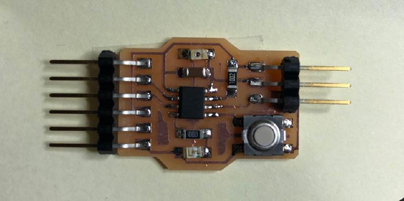
Soldering went without too much trouble. Only thing was, I got the orientation of both the LED and the sensor wrong. I noticed they both had a blue/green marking at one side. Even though inituitively, I felt that that would be the GND side, I went against my better judgement and decided that the unmarked side would be GND. Wrong decision, so I had to desolder these. That was easier that I thought, I just held the PCB board with a pincet by the component that I wanted to remove and pointed the hot gun at it. When the solder melted, the PCB fell off.
After correcting my mistake, I now had my first self designed, self milled and self stuffed Hello World board.

Testing
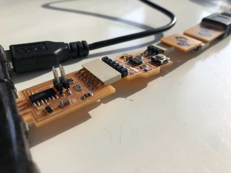
To test the board, I connected it via the FTDI connection to see if it would show up as a USB port, which it did. Then I connected the UPDI connector, to see if I could program the board. That also worked.
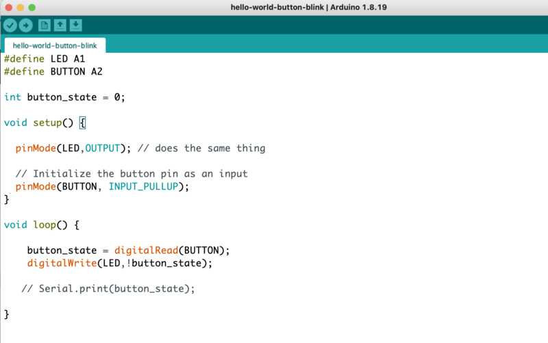
I wrote a very simple program to blink the LED and uploaded it. That didn’t work. To see what was going on I checked if the LED was working with the multimeter, which it did. Then I checked with the multimeter wether the LED got a signal from the controller. It didn’t. As it turned out, the problem was in my code: I used the wrong designator for the pin. After correcting that, the LED worked fine.
looking back
lessons learned
KiCad
A --> Add symbol
R --> Rotates the selected component
X --> flips the selected component
E --> symbol/label properties dialog
Option+3 --> 3D View in the PCB editor
Mods
sources
here are the files for this week