Electronics Production. This week we are going to solder and to mill our own boards. Mindblowing, to be able to create these small worlds with tiny copper roads and small condensator houses. I am looking forward to this, ever since the bootcamp week when we did Erwin’s solder intro.
to learn / to do
Group assignment:
- Characterize the design rules for your in-house PCB production process: document feeds, speeds, plunge rate, depth of cut (traces and outline) and tooling.
- document your work (in a group or individually)
- Document your work to the group work page and reflect on your individual page what you learned
Individual assignment:
- Make an in-circuit programmer that includes a microcontroller by milling and stuffing the PCB, test it to verify that it works.
looking ahead
what I already know
I don’t know too much about electronics. I know about boards, resistors and condensators. I understand there is a microcontroller involved. And I understand that the traces on a PCB board connect all the elements. But there it stops. Why what connects to what, why there are so many resistors and how you know which one you need, this I don’t know.
I have some soldering experience, but that was using a torch and silver solder (long ago when I was studying to be a goldsmith). But I do understand the mechanics of it, and I also played a lot with soldering irons as a kid.
what I want to learn
Ultimately I want to be able to design my own boards, but that is not for this week. I can not imagine that I will ever really be able to design a board, because it all looks like magic to me. But we’ll see. This week, I want to learn to solder the components on the board, nicely and neat. And I want to get to know the cnc mill.
the process
PCBs
The week started as usual, with a lecture by Neil. And some more in depth explanation the next day by Henk. He showed a couple of PCBs (Printed Circuit Boards) and explained their use. It was confusing, with a lot of abbreviations. FTDI, UPDI, SAMD. It took me a while to get a rough idea of what we were supposed to do, and how it all connected. But I got it down to this:
FTDI
We are going to make a FTDI board. FTDI is a company, and they create hardware that converts between serial communication and USB. This FTDI board will enable us to have serial communications with hardware and other PCB’s, via the USB port of the computer.
Serial to UPDI
Then there is a small connector board. This connects to the FTDI with a 6 pin header. And had a 3 pin header at the oher side. This board is a bridge between the serial output of the FTDI to UPDI.
UPDI
Unified Program and Debug Interface (UPDI). This is an interface to program ATtiny microprocessors. I guess I can create a board with a ATtiny microprocessor in the future, and use the FTDI and its converter to program it.
SWD
A programmer interface for SAMD11C microprocessor.
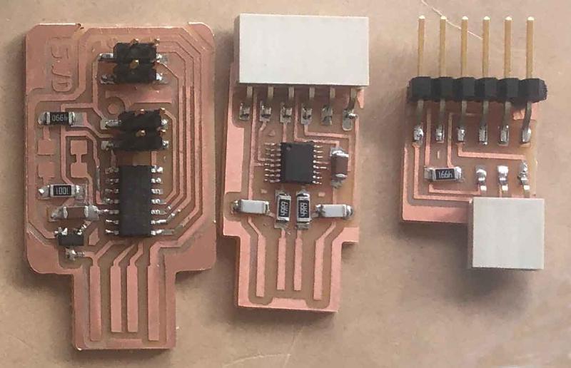
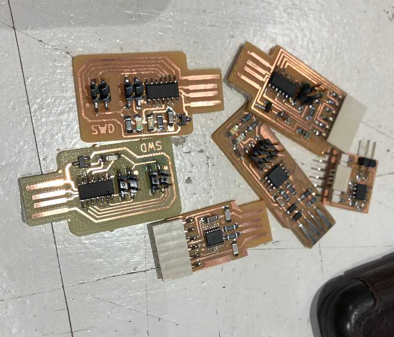
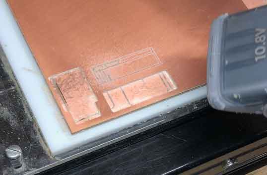
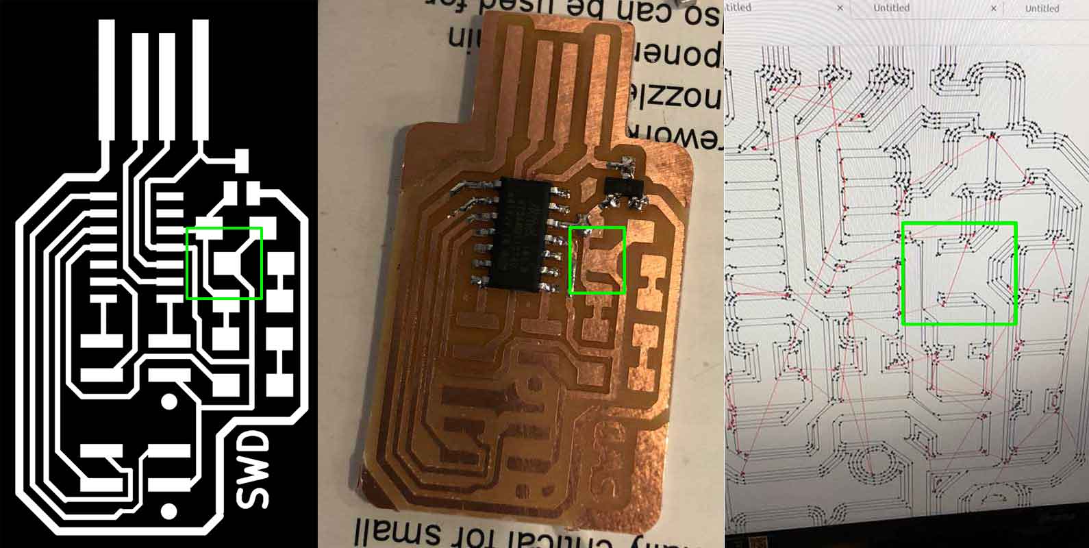
Below is an image of the boards we could make this week. I made the ones in the green outlines. To the left there are two FTDI boards, then the connector, and to the right is the SWD programmer.
PCB milling
Then an explanation of the CNC mill.
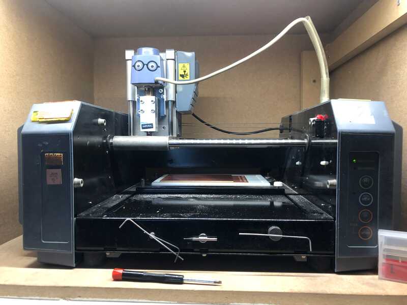
At Waag we use a Roland Modela MDX-20 . It can mill in 2d, but also in 3d. For PCB milling we will use its 2.5d milling capacities.
The mill consists of the following elements:
a milling head
The head contains a spindle and the spindle holds the milling bit. The head is supported by one axis, that moves the head on the Y axis to get the head into position. The head itself moves along the Z-axis, for the cut depth. The X axis movement is handled by moving the milling bed.
a milling bed
This is where the material to be milled goes. This bed consists of several layers. From bottom to top they are:
- Acrylic base
- Acrylic plate on top of the base. This plate is milled level by this mill, so that it is precisely flat and level with the head
- Sacrifical copper plate. This plate serves as an underlayer of the plate that will be milled. Its function is to protect the acrylic plate below it from milling into it.
- Plate to be milled. We will use FR1 for milling. This is a board material that consists of resin and cardboard, with a veeeeery thin layer of copper on top.
Preparing the sacrificial layer
When the plate for milling is done for, it needs to be replaced by a new plate. This process goes as follows:
- unscrew and get the white acrylic bottomlayer out of the mill bed
- get the old plate off (with a sharp putty knife)
- clean the sacrifical layer with sticker remover, make sure it is clean and flat
- get a fresh plate and tape 6 doublesided pieces of tape to its bottomside
- push the plate on to the sacrifical plate
- push it reaaaalllly reaaally tight
- put the white acrylic bottomlayer back in the mill and screw it (but not too tight)
About drilling bits
There are 2 thicknesses of bits we use. There is the 0.8mm bit to mill the board outline. This bit will go through the material. And there is a 0.39mm bit that is used to mill the traces. This bit only mills through the copper layer of the board. The 0.39mm bit comes with one or two flutes. A flute is the cutting edge of the bit. More flutes means more precise milling.

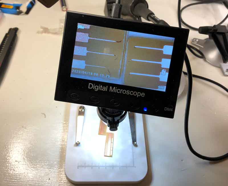
Mods and gcode
The control the milling process, we use Mods (again). It is starting to make sense, as all machines we are using have kind of the same double (sometimes triple) axes operation. Fellow student Bas explained to me that Mods in fact generates a simple sort of instruction set/program, in gcode. Fellow student Saco recognized this gcode immediately as a tried and tested cnc programming language.
You can export and save the gcode that Mods generates. But it can also be sent via a socket-server to the machine, this is the setup that we use for both the cnc mill as the vinyl cutter.
Group assignment
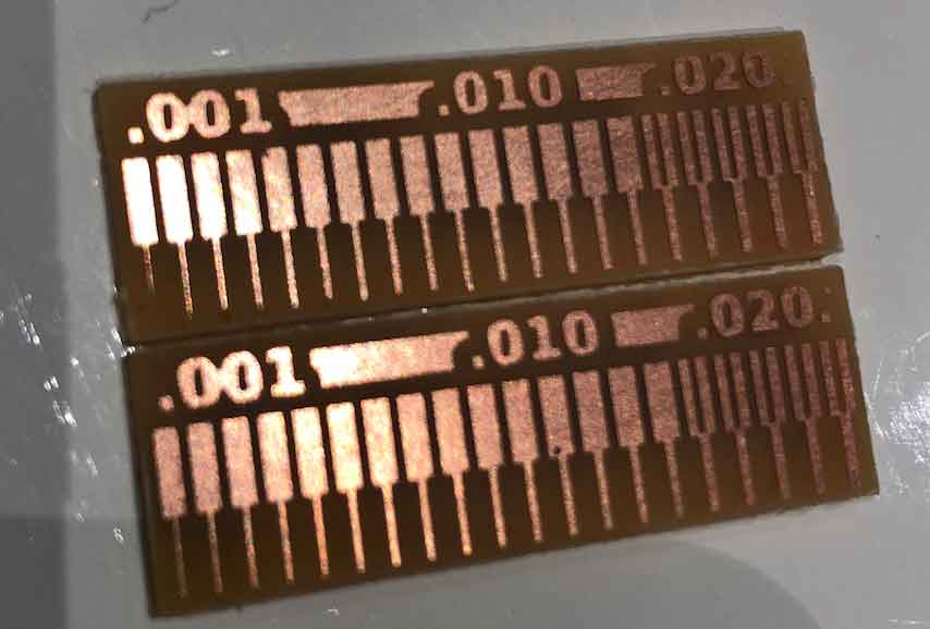
For the group assignment, we divided in two groups. Each group milled a test pattern, with a different bit. Our group used the two flute bit.
Below is the the test pattern. The scale is in inches, and the most left line is 0.001". The line most right is 0.020" which means each line is 0.001".

Milling the pattern
The result. On the right is the board from our group, milled with the two flute bit. It is much more precise and has more detail than the one flute bit. The thinnest line of 0.001" is done well, which means in that 0.025mm is the smallest line our machine can produce with the two flute bit. With the one flute bit this is 0.005", which comes down to 0.13mm.
Below you can see the two boards as well. The fifth line from the right is splitted by a gap, but the others are not any more. That means that the fifth line on the left is the limit of what our machine/tool can trace in regards of the smallest gap. That one is the 0.016" one, which converts to 0.41mm. That is also the diameter of the bit we used, so that makes sense.
Milling a PCB
The process of milling a pcb consists of 2 main steps: first milling out the copper traces, and after that milling out the board itself.
Milling the traces
Turn on the milling machine. If it starts in View mode, set it to Mill mode. Use the 0.39 bit for this. Carefully place it in the spindle, it breaks easily! Tighten the spindle.
- Turn on the machine
- Turn on Mods
- Before touching anything, scroll in Mods to the Socket connection module and close the socket. Close the port. Open the socket. Open the port. Now Mods and the machine should be aware of each other.
- Move the milling head to a place on the board where there is enough space to mill out your PCB. This is done with Mods, by guessing x and y positions and putting these values in the origin fields. Press “Move to origin” and keep adjusting until satisfied.
- Level the mill bit: untighten the screw in spindle untill the bit rests on the copper surface. Make sure the bit does not fall onto the surface, direct it with your fingers. Press the copper surface very lightly for the best milling results. Tighten the screw.
- Load the traces design into Mods. Check the resolution, it should be 1000dpi.
- Click the “Mill Traces” button in the “set PCB defaults (mm)” module in Mods. This copies the settings to the “Mill raster 2D” module
- Adjust the settings:
- Use 0.0025 inches as cut depth (instead of 0.004 inches)
- Set the speed to 4
- Press “Calculate” and inspect the traces outline file
- Press “Send File” in the Websocket Serial Module
If all went well and the mill is listening to Mods, it will start milling. Listen to the sound of the mill. It should sound like it it actually scrapes material. If it sounds too ’light’ chances are it is not levelled correctly or broken.
 I solved it by scraping away the excess copper.
Milling the outline
For the outline, the process is more or less the same, but with different parameters:
- Load the outline file into Mods. This is usually called “interior” even though it creates the outline
- Click the “Mill Outline” button in the “set PCB defaults(mm)”
- Adjust the settings:
- Use 1.55mm as MAX depth (instead of 1.82mm) [important:do not change the CUT depth above it ]
- Change the bit to 0.8mm
- Press “Calculate” and inspect the traces outline file
- Press “Send File” in the Websocket Serial Module
Now the bit mills through the material. When it is finished you can pry out your board with a small screwdriver or knife. Wash it with water and soap, it is now ready for soldering.
Soldering
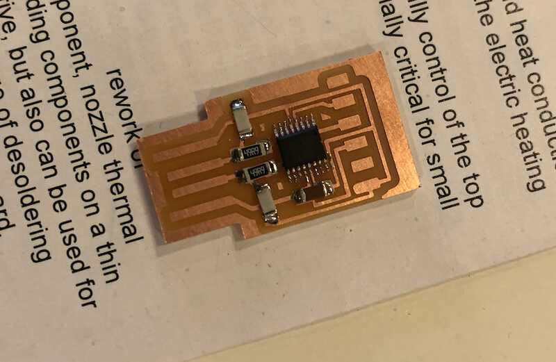
The soldering was a nice zen experience and I enjoyed it a lot. I used the magnifying lamp and a Weller WES51 soldering station. I practiced the things we had learned during bootcamp week; first tinning a pad, then adding the element, let the solder flow again to connect it to the pad. Solder the other side.
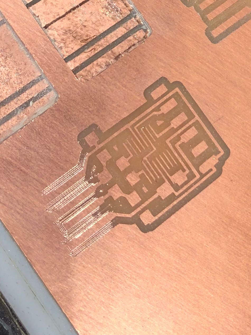
For the tiny FT230 microprocessor of the FTDI, I used flux and a little bit of solder on the iron to solder all the tiny legs.
I used the documentation, and espacially this image to figure out what went where:
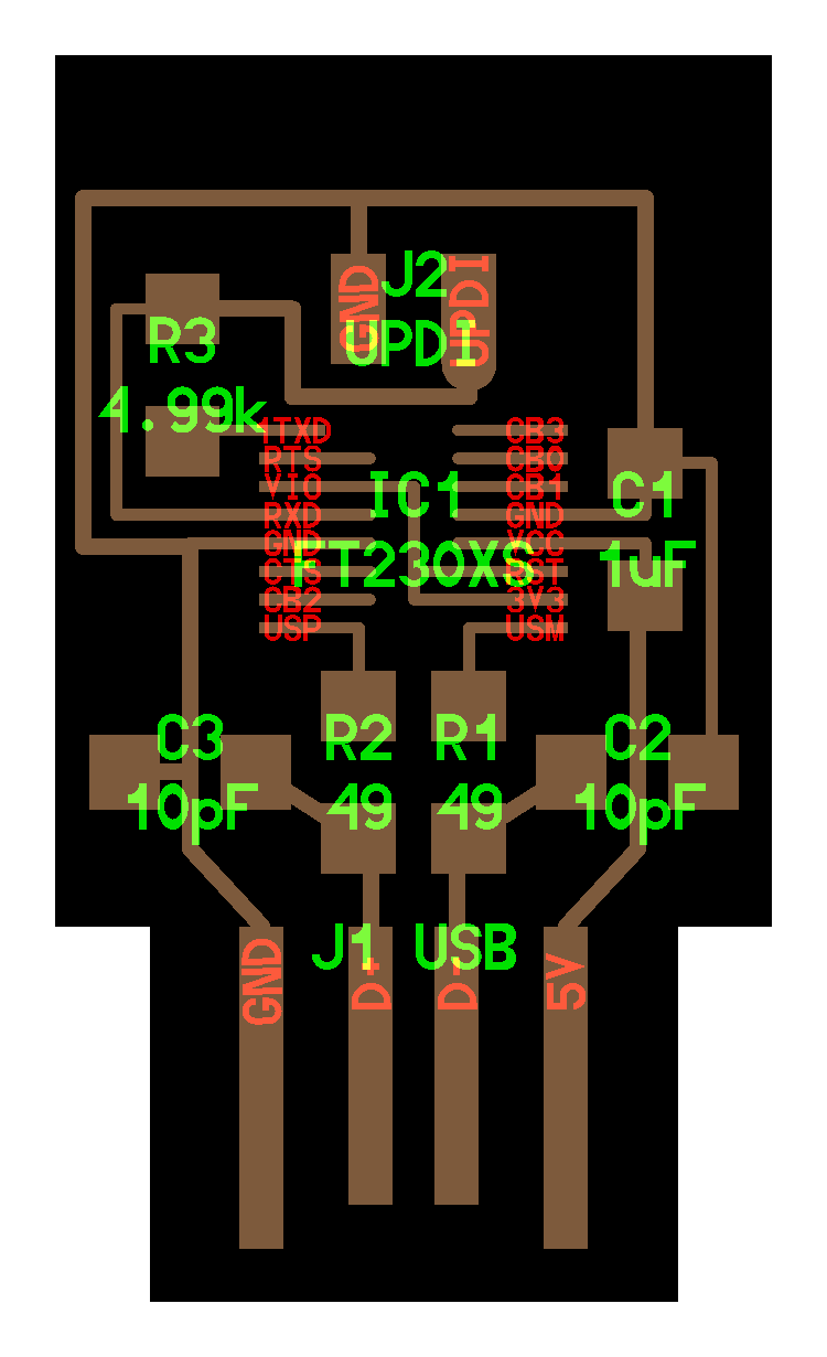
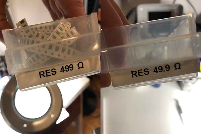
IC stands for Integrated Circuit (the microprocessor), J stands for header/connector, R means Resistor, and C means Condensator. The number directly behind the letter is just for differentiating them from each other. The number below the letter is important, you need it to pick the right component from the inventory. Pay special attention to the many resistor values, as they look deceptively alike.
Testing
FTDI
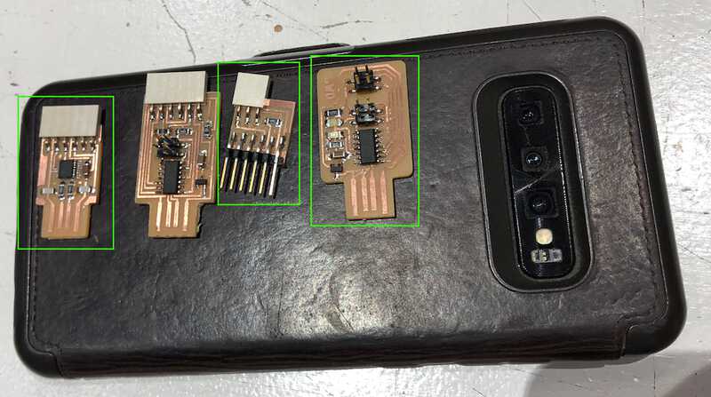
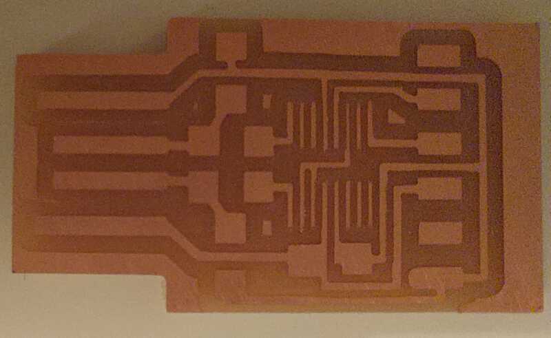
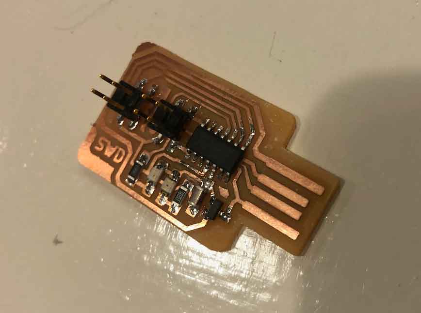
After soldering it was time for testing! But not before I scraped off some excess copper at the outsides of the USB connector. Below is the image of the cleaned up SWD Programmer I made.
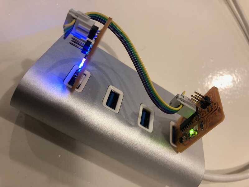
First, I tested the FTDI. For this I connected it to a USB-hub.
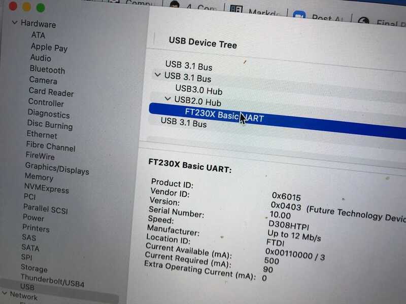
Since I use a macbook, I clicked “System Report” under “About this Mac”. There I got the whole hardware list, and I navigated to USB. I did not see the FTDI immediately, but after refreshing (command R) it showed up.
SWD
Next step was to get the SWD Programmer to work.
For this process, I used the documentation at https://gitlab.fabcloud.org/pub/programmers/programmer-swd-d11c
I connected the board to my USB and was greeted with a green light, meaning the circuits were good and the poard got power. It did not show up in the USB overview though. This was because this board still had ‘no brain’ and needed to be flashed first.
For this, it needed to be connected to another SWD programmer. I connected to Henk’s SWD programmer, and he made sure his ‘out’ header went to my ‘flash’ header. See the image below. The one with the green LED is mine, Henk’s SWD has the blue LED
For flashing, I used OpenOCD, which I installed with brew
brew install openocd
OpenOCD needed a config file openocd.cf that was not present in the documentation. I found an example by googling the chipname and the filename: “SAMD11C14A openocd.cfg” and found a openocd.cfg in a repo that looked like it was the base of the repo I was working with:
https://dma.cba.mit.edu/pub/hello-world/atsamd11/-/blob/erik_test/bootloader/openocd.cfg
I changed the file to point to the correct .bin :
interface cmsis-dap
set transport swd
set CHIPNAME at91samd11c14a
source [find target/at91samdXX.cfg]

init
targets
reset halt
at91samd bootloader 0
program free_dap_d11c_mini.bin verify
at91samd bootloader 4096
reset
shutdown
and ran the openocd command
> openocd

[...]
** Programming Started **
Info : SAMD MCU: SAMD11C14A (16KB Flash, 4KB RAM)
** Programming Finished **
** Verify Started **
** Verified OK **
Flashing seemed to have gone well. I checked USB in the System Report and found:
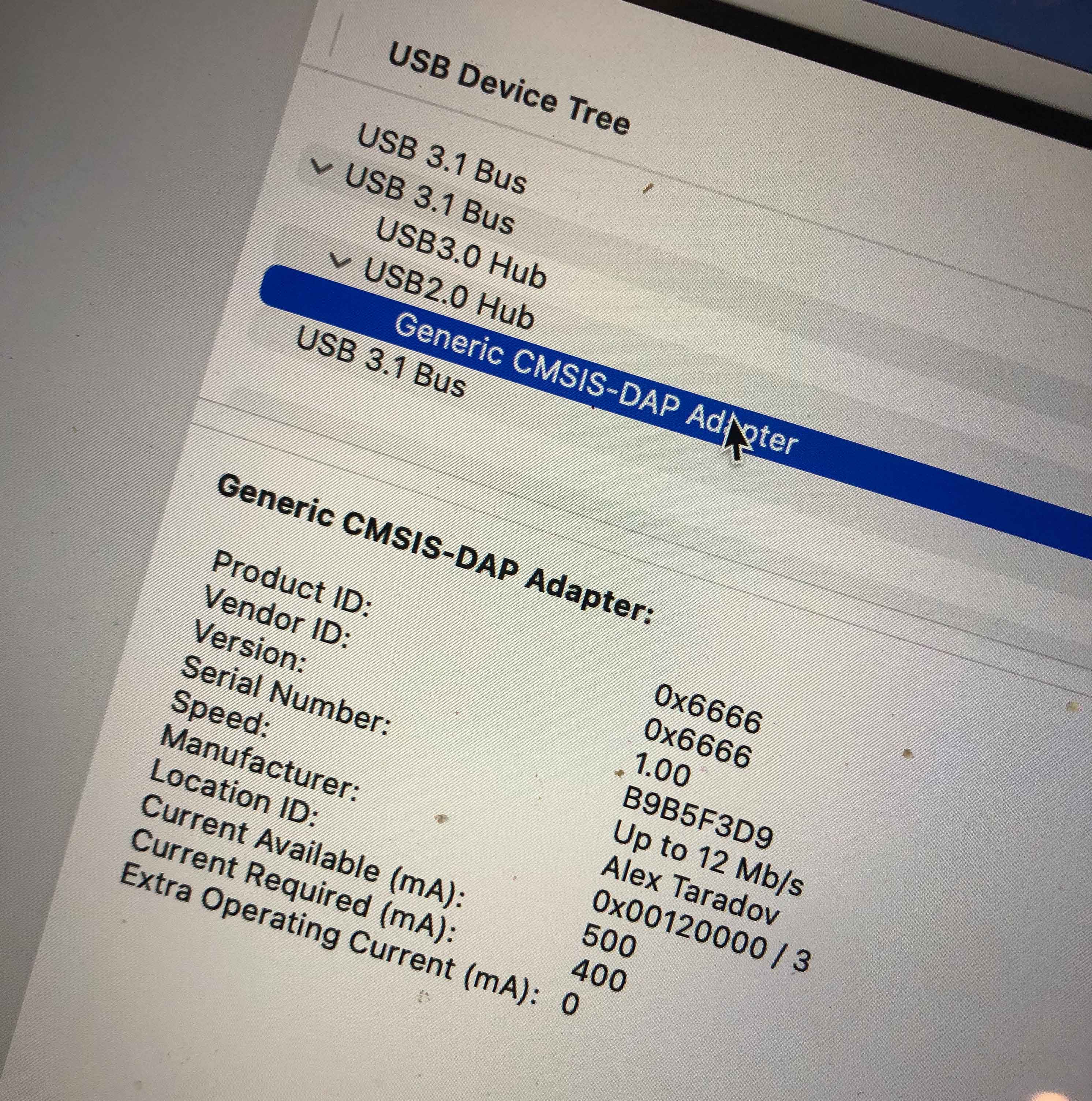
Now the board is ready to use as a programmer.
I read the last of the page on https://gitlab.fabcloud.org/pub/programmers/programmer-swd-d11c/-/tree/main and it finally began to dawn what I had done, and why that was important. With this programmer, I could now flash a bootloader on to a target board. After that, the target board would be accessible directly via USB and I could program it with the ARDUINO ide, as I would a commercial Arduino board.
looking back
what went wrong, what went well
This week was a lot less stressful than the previous two weeks. I had all of my milling and most of my soldering done on friday. On monday I finished the soldering of the last two LEDS and tested the boards. Tuesday I spent on documentation, and also finsihing up documentation of the last two weeks. I also spent some time styling this documentation site.
Most of the work went smoothly. I am happy that I did most of the work on friday. I broke only one bit.