6. Electronics design

Weekly Assignment Requirement
Group assignment:
- Use the test equipment in your lab to observe the operation of a microcontroller circuit board (in minimum, check operating voltage on the board with multimeter or voltmeter and use oscilloscope to check noise of operating voltage and interpret a data signal)
- Document your work to the group work page and reflect on your individual page what you learned
Individual assignment:
- Redraw one of the echo hello-world boards or something equivalent, add (at least) a button and LED (with current-limiting resistor) or equivalent input and output, check the design rules, make it, test it. Optionally, simulate its operation.
Have you answered these questions?
- Linked to the group assignment page
- Documented what you have learned in electronics design
- Explained problems and how you fixed them, if you make a board and it doesn’t work; fix the board (with jumper wires etc) until it does work.
- Included original design files (Eagle, KiCad, etc.)
- Included a ‘hero shot’ of your board
- Loaded a program and tested if your board works
What I’ve done this week
Group assignment:
Individual assignment:
-
Design an electronic circuit using Kicad and save it as svg
-
Export svg in mods as rml so that it can be processed by SRM20
-
Create a board with SRM20
-
Soldering parts to the board
-
Write the program to the board
Design an electronic circuit using Kicad and save it as svg
This time I redraw the board hello.t412.echo (ATTiny412) with LEDs and buttons
I have been using Eagle, but I have decided to try Kicad from this time 🔥
I used Kicad version 6.0.0. You can download it here
Set Kicad environment
Installing Kicad installed multiple related apps!

This time I used the following two main apps

Eeschema: Schematic Layout Editor
Pcbnew: PCB layout editor
The library of electronic parts used in this assignment was downloaded from here
Or clone this repository and rename the directory to fab.
% git clone https://gitlab.fabcloud.org/pub/libraries/electronics/kicad.git
Run KiCad

Go to “Preferences / Manage Symbol Libraries” and add fab.kicad_sym as symbol library.

Go to “Preferences / Manage Footprint Libraries” and add fab.pretty as footprint library.

Go to “Preferences / Configure Paths” and add variable named FAB that points to the installation directory of the fab library

Done🔥
Do Schematic Layout with Eeschema.
First, I created a schematic layout using Eeschema
The tool layout is shown below


Click “Add a symbol”
Type “fab” to see the parts of the library I just added

| Parts | Description | Quantity |
|---|---|---|
| microcontroller | ATTiny412 (SSFR) | 2 |
| LED | Red | 1 |
| Resistor | 1kΩ | 1 |
| Pin Header | 1×2 (UPDI) | 1 |
| Pin Header | 1×6 (FTDI) | 1 |
| Capacitor | 1μF | 1 |
| Button | Tact switch | 1 |
Add the necessary parts.

Click “Run footprint assignment tool” then Click “Anotate”
Annotation is a function that assigns reference numbers to symbols placed in a schematic.
For example, resistors are often used in schematics, and are usually assigned sequential numbers such as “R1,” “R2,” etc., but as they are deleted or added during circuit creation, the numbers become jumbled.
KiCAD’s “Annotation” function can be used to automatically assign reference numbers

The footprint Assignment is displayed.
Click “OK” for the following settings


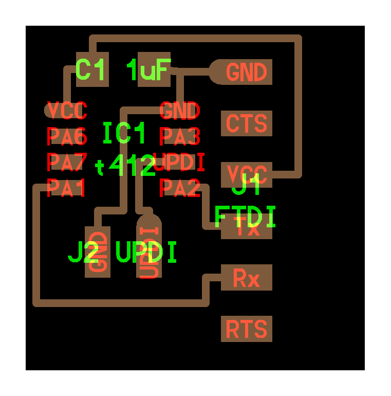
Wired it as follows

Things to keep in mind when wiring
Add a No-connection-flag for lines you do not use

You can connect all the wires together, but “net label” makes it easier to understand the wiring.

It is easy to understand if each part is grouped by function or type using connected graphic lines.

“Power_PWR_Flag” indicates that “Vcc” and “GND” are the power supply. “Power_PWR_Flag” is a component that specifies that it is a power supply, not an actual component.

Run ERC” to check for errors and warnings.

Done 🔥🔥🔥
Export .net format to open in Pcbnew
File => Export => Netlist => Export Netlist

Do PCB layout with Pcbnew
The tool layout is shown below

Import the netlist I just created.

The wiring setup is as follows
Select File => board setup => Net Classes

For Class net selection, Power is selected for VCC and GND, and Default is selected for others.
| Net Class | Clearance | Track Width | Via Size | Via Hole | uVia Size | uVia Hole | DP Width | DP GAP |
|---|---|---|---|---|---|---|---|---|
| Default | 0.4 mm | 0.4 mm | 0.8 mm | 0.4 mm | 0.3 mm | 0.1 mm | 0.2 mm | 0.25 mm |
| Power | 0.4 mm | 0.8 mm | 0.8 mm | 0.4 mm | 0.3 mm | 0.1 mm | 0.2 mm | 0.25 mm |
Wired on F.Cu layer as follows
Can also route under microcontroller, resistors, capacitors, and buttons

Create a board shape on the Edge cuts layer

Run DRC” to check for errors and warnings.

No error was displayed, but a warning appeared I ignored this time because warnings do not cause circuit errors.
File => Export => SVG
Select “F.Cu” and “Edge.Cuts”, click “Export”

Export svg in mods as rml so that it can be processed by SRM20
After opening the svg file in the mods, click “invert” in the “convert SVG image” to invert the black and white

Create a board with SRM20


Done🔥🔥🔥
Soldering parts to the board
I used parts from lab Inventory, soldered them and tested the board.

Assembled🔥🔥🔥

After soldering, I used a multimer to check the electrical circuits
This time it was done with one soldering👍
Write the program to the board
Write the following program and make serial communication with the board I have created.
#define max_buffer 25

static int index = 0;
static char chr;
static char buffer[max_buffer] = {0};

void setup() {
  Serial.swap(1);
  Serial.begin(115200);
}

void loop() {
if (Serial.available() > 0) {
  chr = Serial.read();
  Serial.print("hello.t412.echo: you typed \"");
  buffer[index++] = chr;
  if (index == (max_buffer-1))
    index = 0;
  Serial.print(buffer);
  Serial.println("\"");
  }
}

Write the program on my board

Message Area Details
SerialUPDI
UPDI programming for Arduino using a serial adapter
Based on pymcuprog, with significant modifications
By Quentin Bolsee and Spence Konde
Version 1.2.3 - Jan 2022
Using serial port /dev/cu.usbserial-DN055FYP at 57600 baud.
Target: attiny412
Set fuses: ['2:0x02', '6:0x04', '8:0x00']
Action: write
File: /var/folders/z5/2y_sk4r946ldl15ybd8fcwk80000gn/T/arduino_build_641049/echo_hello_412.ino.hex
Pinging device...
Ping response: 1E9223
Setting fuse 0x2=0x2
Writing literal values...
Verifying literal values...
Action took 0.19s
Setting fuse 0x6=0x4
Writing literal values...
Verifying literal values...
Action took 0.19s
Setting fuse 0x8=0x0
Writing literal values...
Verifying literal values...
Action took 0.19s
Finished writing fuses.
Chip/Bulk erase,
Memory type eeprom is conditionally erased (depending upon EESAVE fuse setting)
Memory type flash is always erased
Memory type lockbits is always erased
...
Erased.
Action took 0.06s
Writing from hex file...
Writing flash...
[==================================================] 8/8
Action took 0.70s
Verifying...
Verify successful. Data in flash matches data in specified hex-file
Action took 0.12s
Done👍
Type “hello” in the text box and it returned “hello” as follows

Done🔥
What I learned
-
This was my first time using Kicad 6.0, and since it was easier to use than Eagle, I decided to use Kicad from this week.
-
I learned a lot about the basics of creating electric circuits, such as the use of pull-up resistors and capacitors.
Links to Files and Code
-
hello.serial-UPDI.3
-
redraw_echo_hello_board
-
Kicad
-
Eeschema
-
tiny412.net (redraw_echo_hello_board) [.net]
-
tiny412.kicad_sch (redraw_echo_hello_board) [kicad_sch]
-
-
Pcbnew
- tiny412.kicad_pcb (redraw_echo_hello_board) [kicad_pcb]
-
![[png]](../files_and_codes/files/week06/hello.serial-UPDI.3.traces.png)
![[png]](../files_and_codes/files/week06/hello.serial-UPDI.3.interior.png)
![[rml]](../files_and_codes/files/week06/hello.serial-UPDI.3.traces.png.rml)
![[rml]](../files_and_codes/files/week06/hello.serial-UPDI.3.interior.png.rml)
![[svg]](../files_and_codes/files/week06/redraw_echo_hello_board_trace.svg)
![[svg]](../files_and_codes/files/week06/redraw_echo_hello_board_interior.svg)