Week 4: Electronics Production
This week is about Electronics production where we have to use PCB milling machine and fabricate the in-circuit programmer. This week will gives us the hands on experiencing with the PCB milling machine and producing of circuit which will later help us build our own circuit for our final project.
Instruction:
Make an in-circuit programmer that includes a microcontroller, mill and stuff the PCB and test it to verify that it works.
Extra Credit:
☞ Customize the design
☞ Try other PCB processes
Group Assignment:
Characterize the design rules for your in-house PCB production process
Extra Credit: Send a PCB out to a board house
- To Do:
- Learn about Milling machine and how to operate.
- Learn about mods and how to make the file for PCB machine.
- Setup the printer and print the circuit board for in-circuit programmer.
- Soldering the components for the circuit.
- Test the circuit if its working.
- Group Assignment.
PCB Milling
In-circuit Programmer is the ability of some programmable logic devices, microcontrollers, and other embedded devices to be programmed while installed in a complete system, rather than requiring the chip to be programmed prior to installing it into the system.
In order to fabricate in-circuit programmer, we have to print the circuit board in the milling machine. The PCB milling machine that we have in the lab is the MonoFab SRM 20.
Specifications of SRM20:
- Workpiece Table Size: 9.14 (X) × 6.17 (Y) in.
- Operating Speed: 6-1800 mm/min (0.24079.87 inch/min)
- X,Y,Z Operation Strokes: 203.2(X) × 152.4(Y) × 60.5(Z) in.
- Mechanical Resolution: 0.000998 mm/step
- Machine Dimensions: 17.76(W) × 16.80(D) × 16.78(H) in.
- Taken from: https://purpleplatypus.com/products/roland-3d-mills/monofab-srm-20/
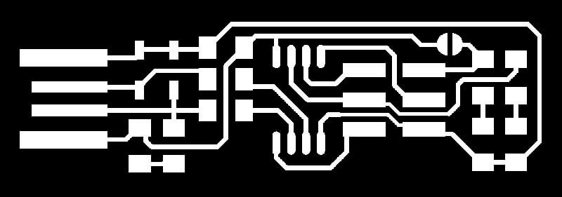
Downloaded the circuit design board from Brians design for both circuit trace and outline cut. After we get the circuit design, it is important to set in the MODs, in order to make file for Miling Machine.
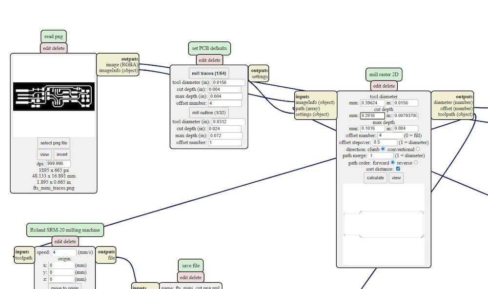
In the Select PNG file from the Read PNG group, select the trace or outline cut file that is downloaded. In the Set PCB Default group, select Mill Traces for printing circuit and select Mill Outlines for cutting the outline of the board.
If the traces don't come out well, increase the max depth by 0.1 under Mill Raster 2D group and run the machine again on the same board.
Setting up milling machine:
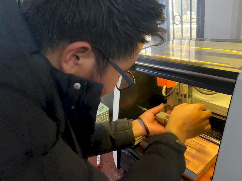
Loose the screw on the collet of the srm machine and insert the end mill of required size (1/64 for milling trace and 1/32 for milling outline). After that, we need to set the X, Y, and Z coordinate to print the circuit.
- Milling Trace detail
- Tool diameter: 1/64(0.0156 in) or 0.39624 mm
- Spindle Speed: 9000RPM
- Feed rate: 240mm/min
- Plunge rate: 0.1016mm
- Maximum depth: 0.1016mm Cutting outline detail:
- Tool diameter: 1/32(0.0312 in) or 0.79248 mm
- Spindle Speed: 9000RPM
- Feed rate: 240mm/min
- Plunge rate: 0.6096mm
- Maximum depth: 1.82879999mm
Move end mill point to the desired coordinate and set X/Y to zero using X/Y under Set Origin Point.
Lower the Z axis nearing to the plate of pcb set on the sacrificing layer. It is important not to take too low or touching the pcb board. After reaching the satisfied point, let the endmill free fall by loosening the screw. Once it touched the pcb board, tighten the screw again and you are good to go. Set the Z-axis zero using Z under Set Origin Point.
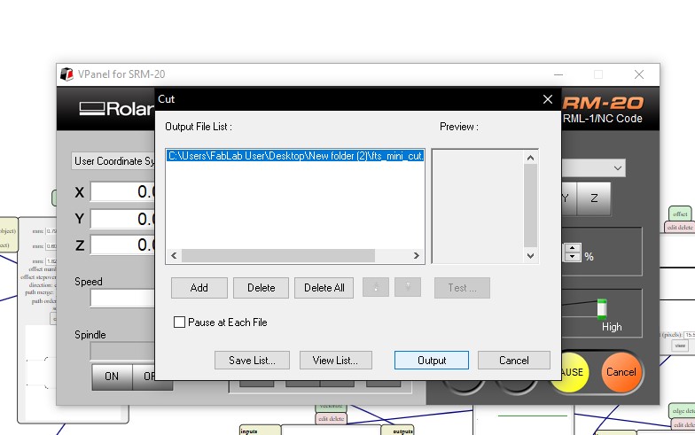
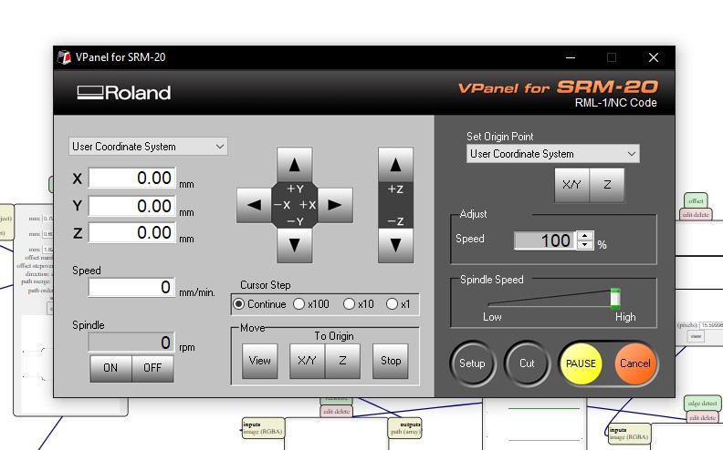
Click on the Cut button and it will navigate to above page. Select the url presented and delete all the selected file. Click on the Add and select the file saved from the MODS. Click on the Output to run the machine.
Milling under process.
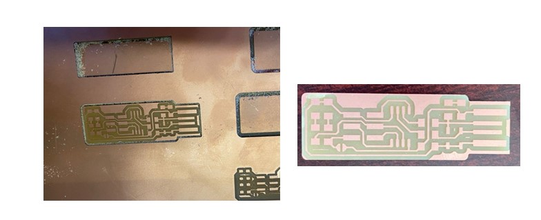
It takes five to ten minutes to mill the traces and four to five minutes to cut the outline. After removing from the base, we need to clean the unwanted left over and getting ready for soldering.
Soldering:
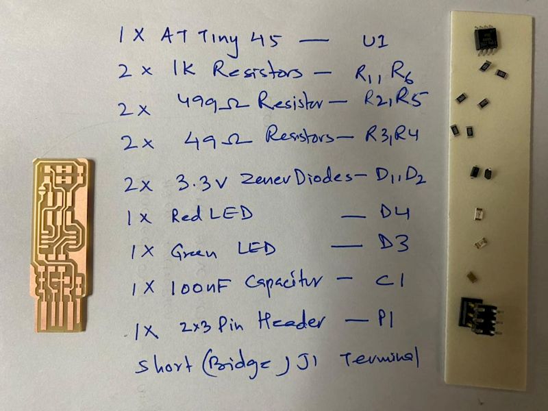
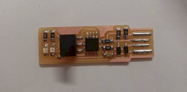
Soldering is the process of joining metal parts to form electrical bonds. It uses a low melting point metal alloy (solder) which is melted and applied to the metal parts of electronic components to be joined and this bonds to the copper parts of the pcb and forms a connection when the solder solidifies.
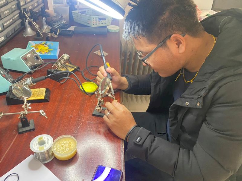
Usually soldering of Surface Mount Device (SMD) components are challenging due to its small size.
- Programming ISP:
- Go to Brians ISP.
- Follow the instruction given under Get and Build the Firmware to install the firmware.
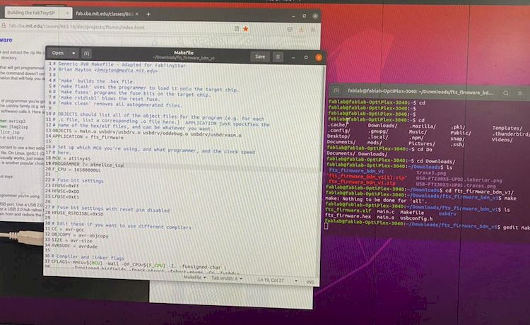
- Using the 'cd' commend to direct to makefile and open the makefile.
- In the makefile, change PROGRAMMER ?= usbtiny as PROGRAMMER ?= atmelice_isp.
- Connect the fabricated chip with the Atmelice_isp.
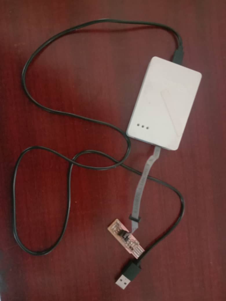
Connect both atmelice_isp usb and fabricated chip to the usb port of the PC. - Run 'make flash' command. This will erase the chip's memory and flash with the .hex file.
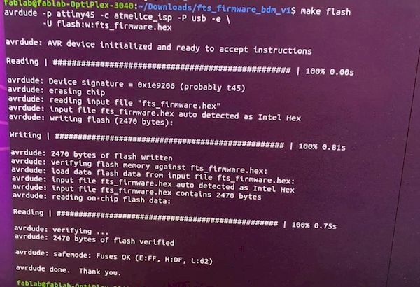
- Run 'make fuses' command if the above work successfully. This will set up all of the fuses except the one that disables the reset pin.
- Now in order to check if it worked, disconnect atmelice_isp (keep the chip inserted) and run 'lsusb' command. If there is Multiple Vendors USBtiny present in the list, it is successful.
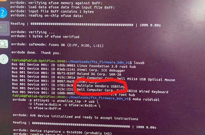
- Now we have to disable the reset fuse. Connect the programmer once again and Run 'rstdisbl'.
- Last thing is to disconnect the junction J1 of the IC.
Once we complete with fibrication and soldering, it is crucial for the program loading in order to make ISP the programmer. Program loading steps are as follow:
Issue:
As most of the issues arises during the soldering and component placing, I made extra careful during the time.
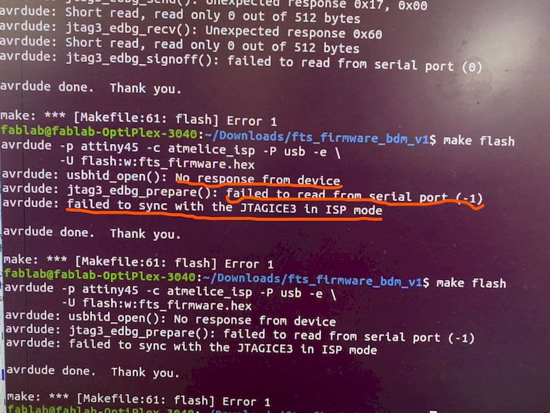
Despite my extra careful, there still came the error during the 'make flash'. I made effort in tracking down the problem and later found out that the terminal of the fabricated isp was not getting well connected to the usb port of the PC. So, I used the tape to make the terminal thicker and it worked.
 Find here
Thank You
Reference
- Fab ISP of Brians http://fab.cba.mit.edu/classes/863.16/doc/projects/ftsmin/index.html
- HTML code reference: https://www.w3schools.com/html/default.asp
- MODS for SRM 20: https://mods.cba.mit.edu/