
Use the test equipment in your lab to observe the operation of a microcontroller circuit board.
Link to Group AssignmentUse an EDA tool to design a development board to interact and communicate with an embedded microcontroller.
Extra credit: try another design workflow.
Extra credit: design a case for it.
Extra credit: simulate its operation.
Assignment Requirement
Status
Linked to the group assignment page
Completed
Documented what you have learned in electronics design
Completed
Explained problems and how you fixed them
Completed
Included original design files (Eagle, KiCad, etc.)
Completed
Included a ‘hero shot’
Completed
For this assignment I used KiCAD EDA (Electronic Design Automation). This software allowed me to design my schematic diagram as well as produce the actual layout that I needed to build my microcontroller development board.
Before I began to design my circuit I had to install Fab Academy KiCAD Libraries in order for the symbols and footprints I used to correspond with the components available to me.
I downloaded the libraries and placed them in a folder which I named Fab.
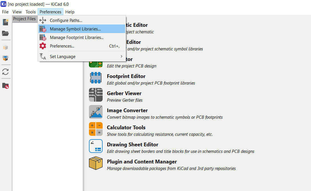
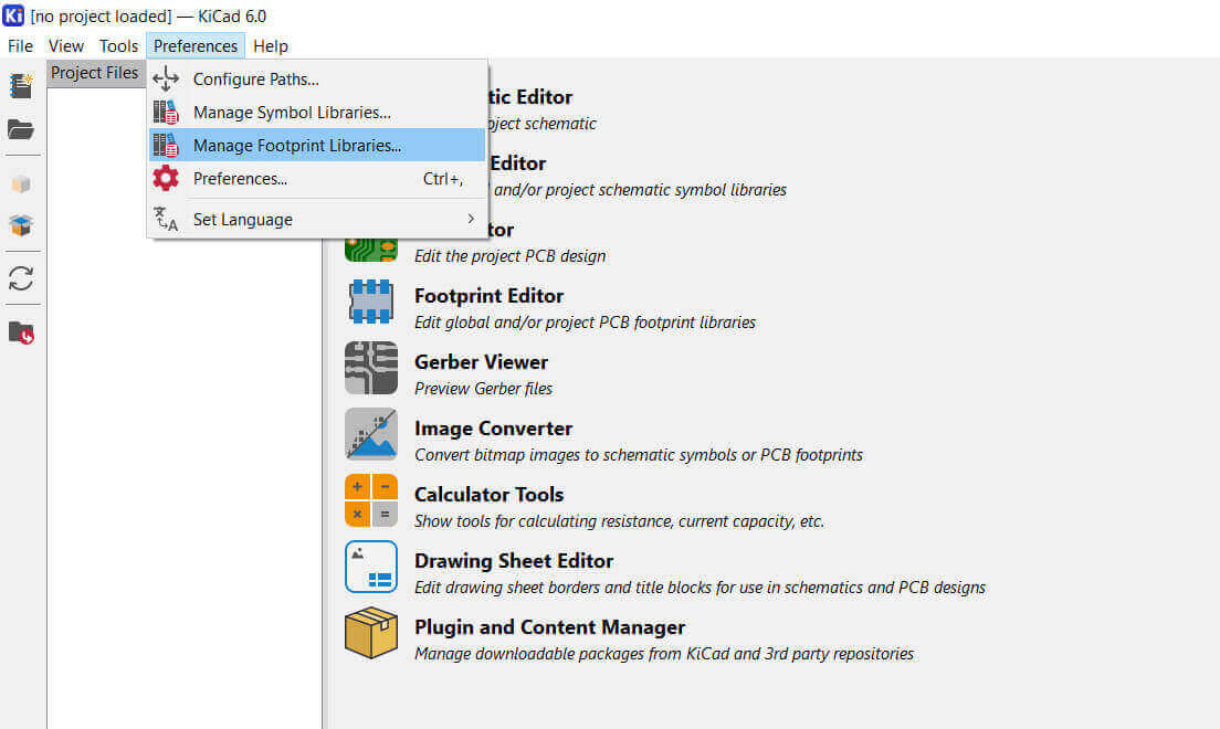
I opened the KiCAD program where I selected Preferences from the menu tab at the top and from the drop-down menu , I clicked on Manage Symbol Libraries.
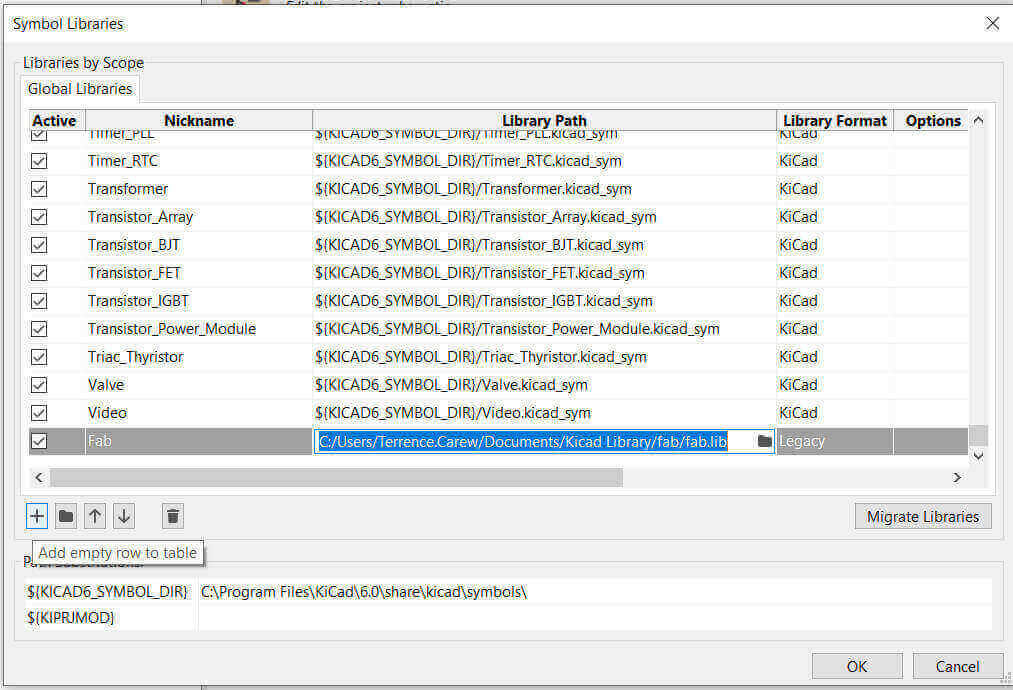
The Symbol Libraries window opened displaying a list of existing libraries. I clicked on the "+" sign at the bottom of the list. This allowed me to add an emty row. I entered Fab for the Nickname so that when I need a symbol from the library I can start the search with the word Fab to narrow the search list because there are thousands of similar components from other libraries. For the Library Path I entered the directory for where I saved the libraries specifically the fab.lib file. The Library Format was set to Legacy.
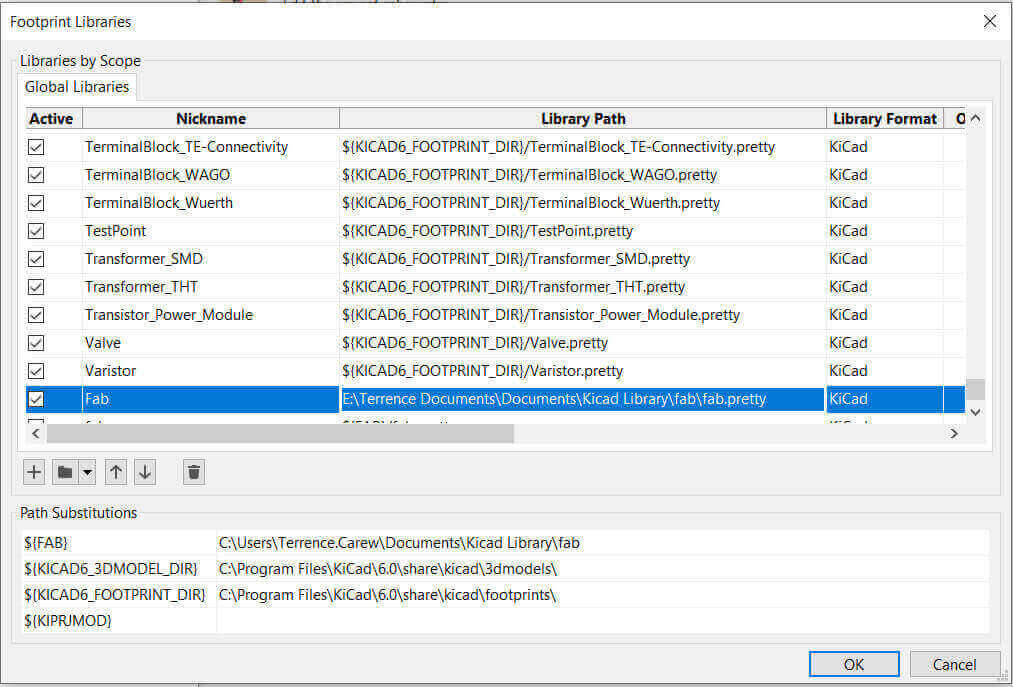
I opened Preferences again and from the drop-down menu I selected Manage Footprints Libraries.
The Footprint Libraries window opened. I clicked on the "+" sign at the bottom to add an empty row similarly to the Symbol Libraries window. I entered Fab for this Nickname also. For the Library Path I entered the directory for the libraries saved specifically the folder fab.pretty. The Library Format was left at default KiCad.
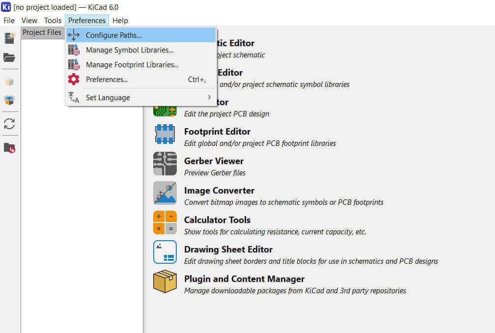
I opened Preferences yet again and this time I selected Configure Paths.
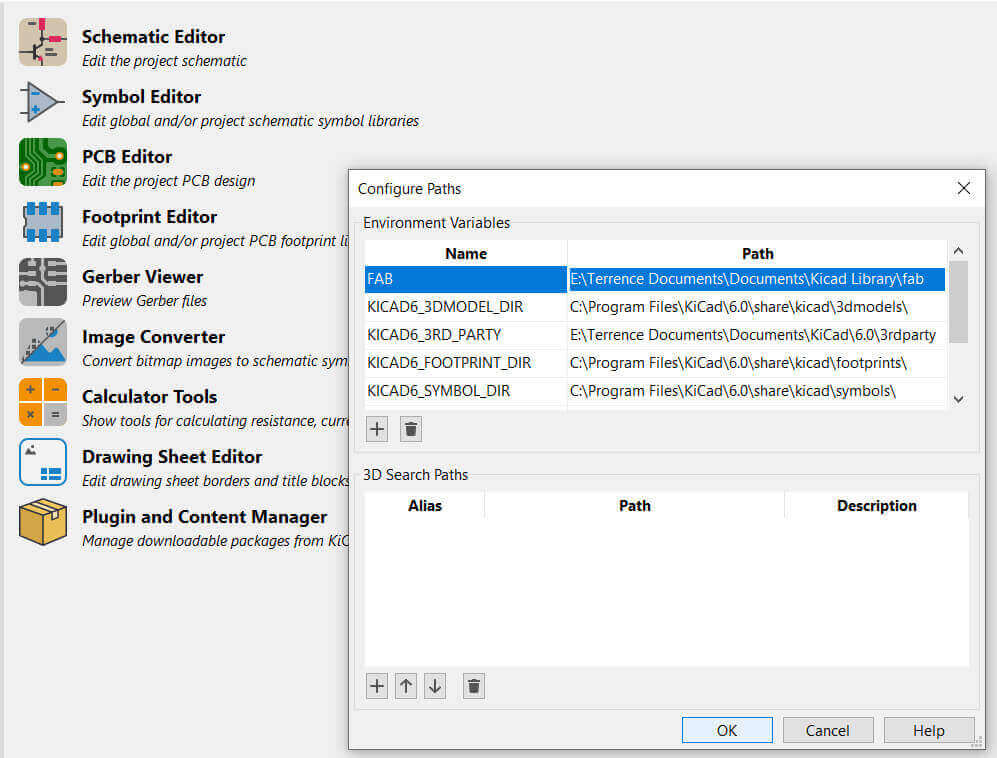
The Configure Paths window opened. I clicked the "+" sign to add empty row. I added the FAB (all uppercase) for the Name and for Path I entered the directory for where I saved the libraries.
I had skipped this step at first and encountered some issues accessing the symbols.
I successfully installed the libraries I needed so now I was able to access the component symbols had to use and I can begin my design. I clicked File from the Menu tab at the top and selected New Project. A window opened allowing me to name and save my project at a selected location.
A Project panel was opened containing two blank files, a schematic and a PCB layout file.
I selected the schematic file which opened in the Schematic Editor. A drawing page was opened with a Title Box at the bottom right corner.
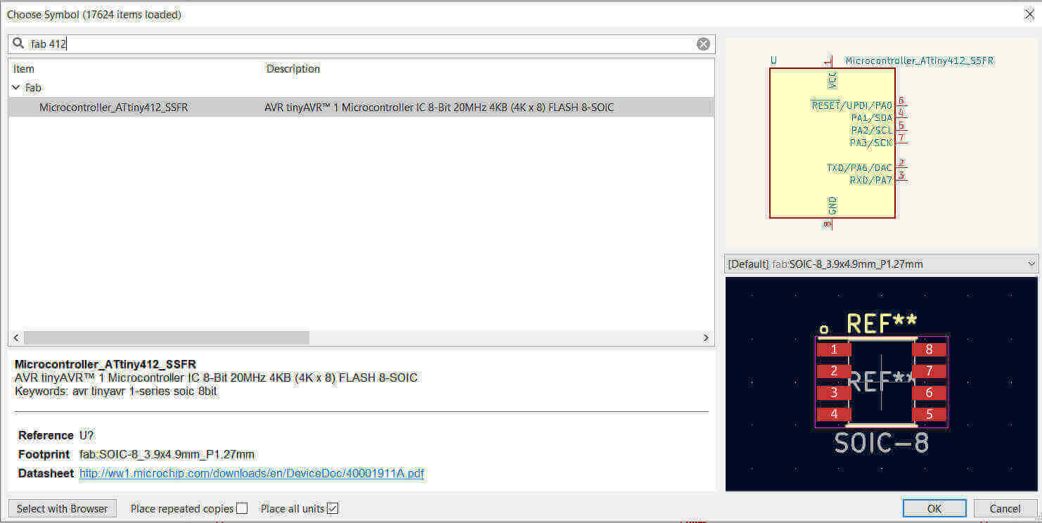
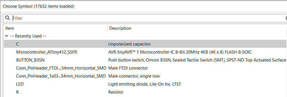
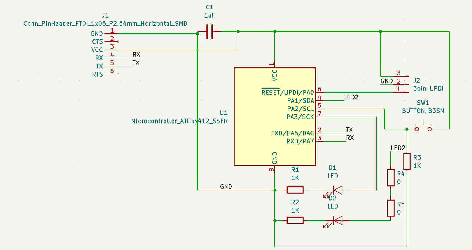
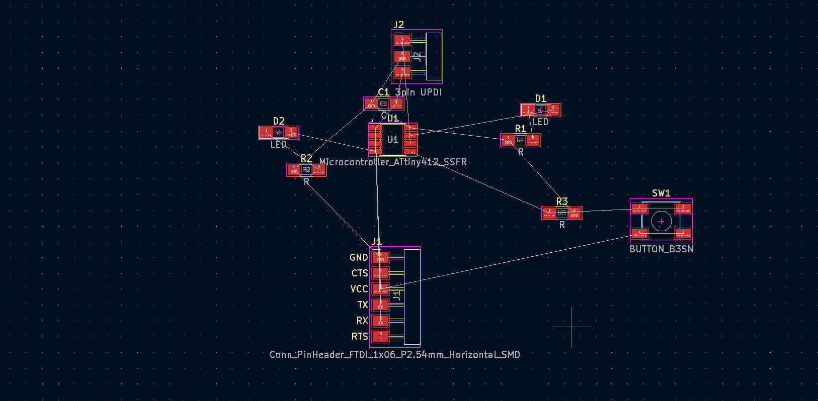
My idea for the circuit included the ATTiny412 microcontroller, two LEDs and a switch. To add components I clicked the Choose Symbol tool (third icon down, looks like a logic gate symbol) from the Tool Panel on the right. I soon learned the keyboard shortcut was "A" which made things a lot faster and easier. These were the main components, however I needed a by-pass capacitor and two ports for the UPDI and Serial connections.
The Choose Symbol window opened. To select my first symbol which was the ATTiny412 I typed "fab 412" in the search bar. I used "fab" to narrow the search and "412" which was part of the name of what I was looking for, I didn't need to be too specific. The window displayed the schematic symbol as well the footprint symbol to ensure that I selected the correct component I needed.
I searched and added all the components I needed to start my schematic.
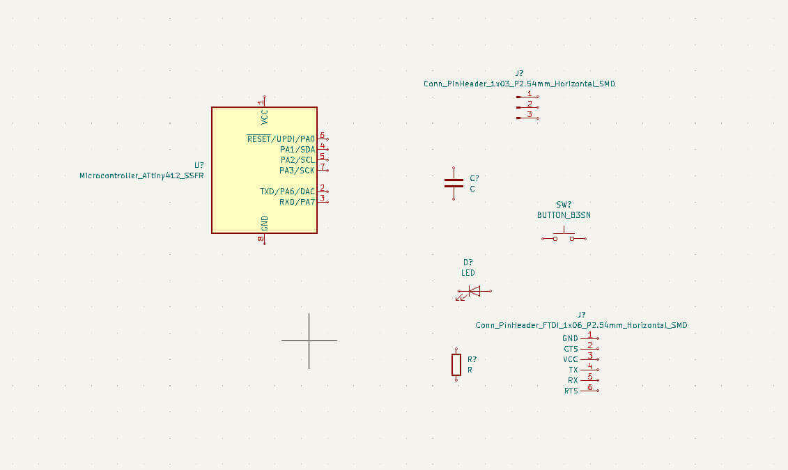
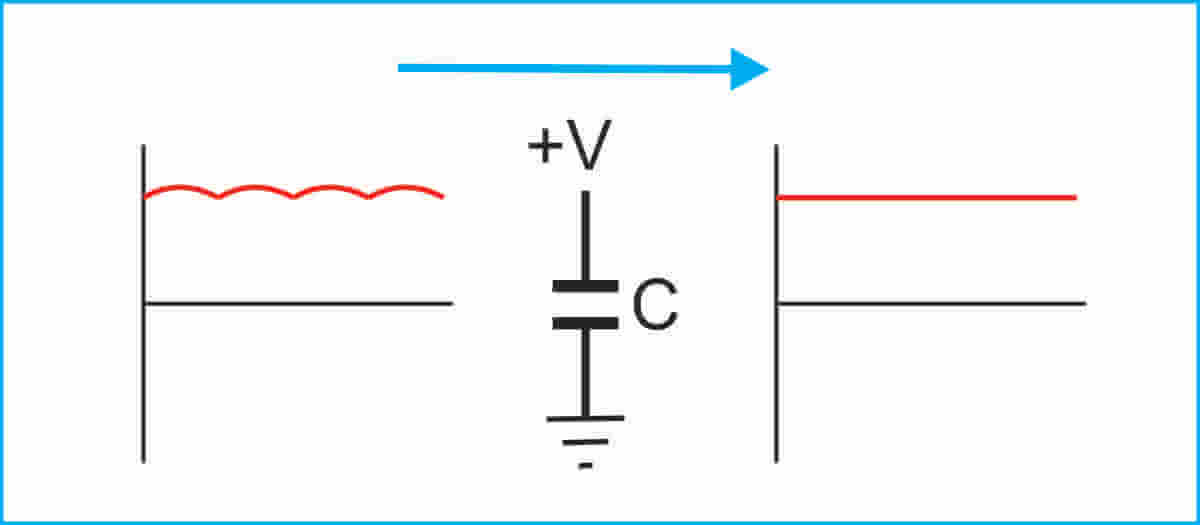
The bypass capacitor was used to smoothen any ripples that may be present in the DC voltage source. Unlike a voltage regulator which increases or decreases the voltage to keep the value constant when there is a drop or spike, the capacitor keeps the signal wave constant. I used a non-polarized 1uF capacitor for the bypass capacitor.
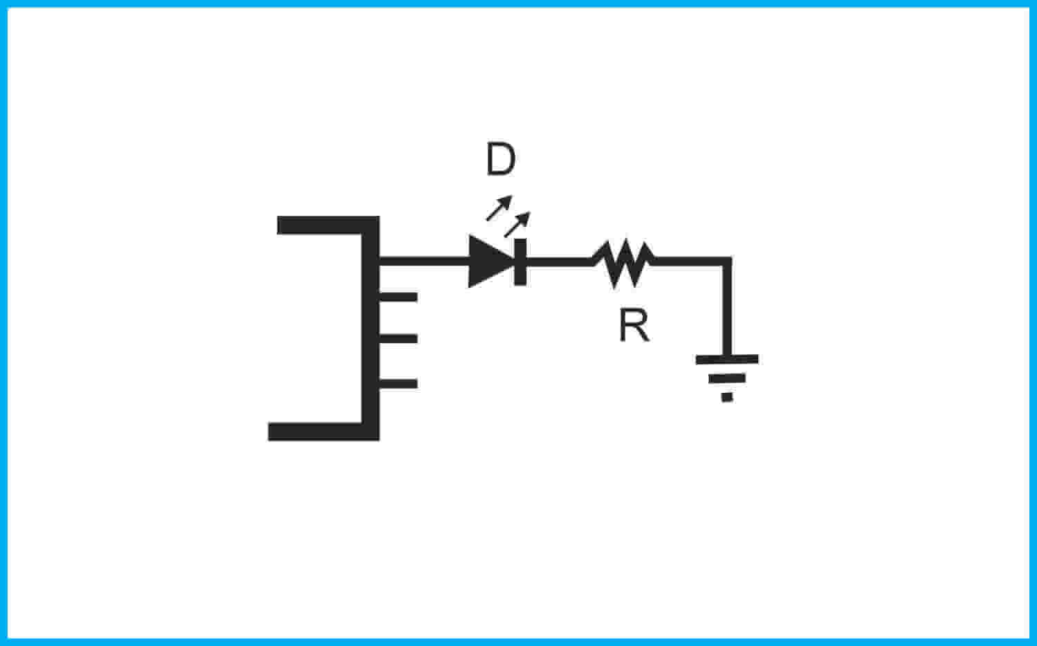
The LEDs I used could only take a maximum of 2.6V, however, the microcontroller outputs 5V so I had to add a limiting resistor in series with the LED. For this I used a 1K Ohm resistor.
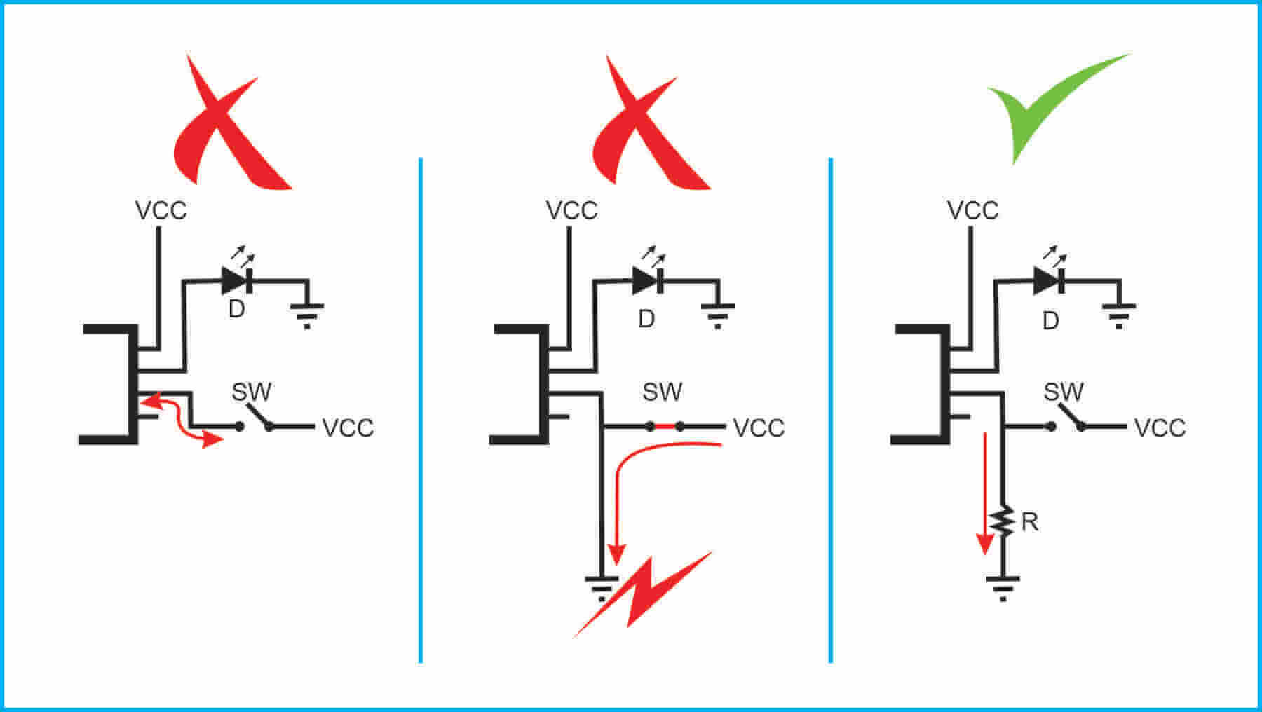
I included an additional resistor to my circuit which served the purpose of a pull down resistor. When I connected the microcontroller pin to the switch, the other end connected to the 5V VCC. I designed it this way so that the pin will be an input and when the switch is pressed it will allow a High signal or 5V to enable the input to power the LEDs or whatever program I run. This seemed simple, however this input pin will become a floating pin. This floating pin means that when the switch is in OFF/Open position, the pin will be rapidly switching between a High and Low signal causing the LED/s to continuously hav a dim flash. To correct this in the design I needed to send a Low signal (0V) to the pin which means I had to connect the pin to ground. Connecting to ground will ensure that a Low signal is sent to the pin when switch is OFF/Open, however, when the switch is ON/Closed the High signal/5V will bypass the pin and go straight to ground (since current flows through the path of least resistance) shorting the circuit. This is where the pull down resistor came in. A1K Ohm resistor was connected between the pin and ground so that there is a pathway for a Low signal to go to the pin when the switch is OFF/Open and NOT a direct pathway for VCC to go to ground when the switch is ON/Closed.
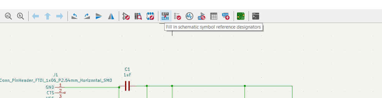
When I added all the components symbols, I had to Annotate the schematic meaning a reference number was assigned to each symbol.
I completed the schematic by making all the required connections using the Wire Tool. I moved the component around by just selecting the symbol and dragging and I rotated the symbol by pressing "R" on the keyboard. To label a symbol I pressed "L".
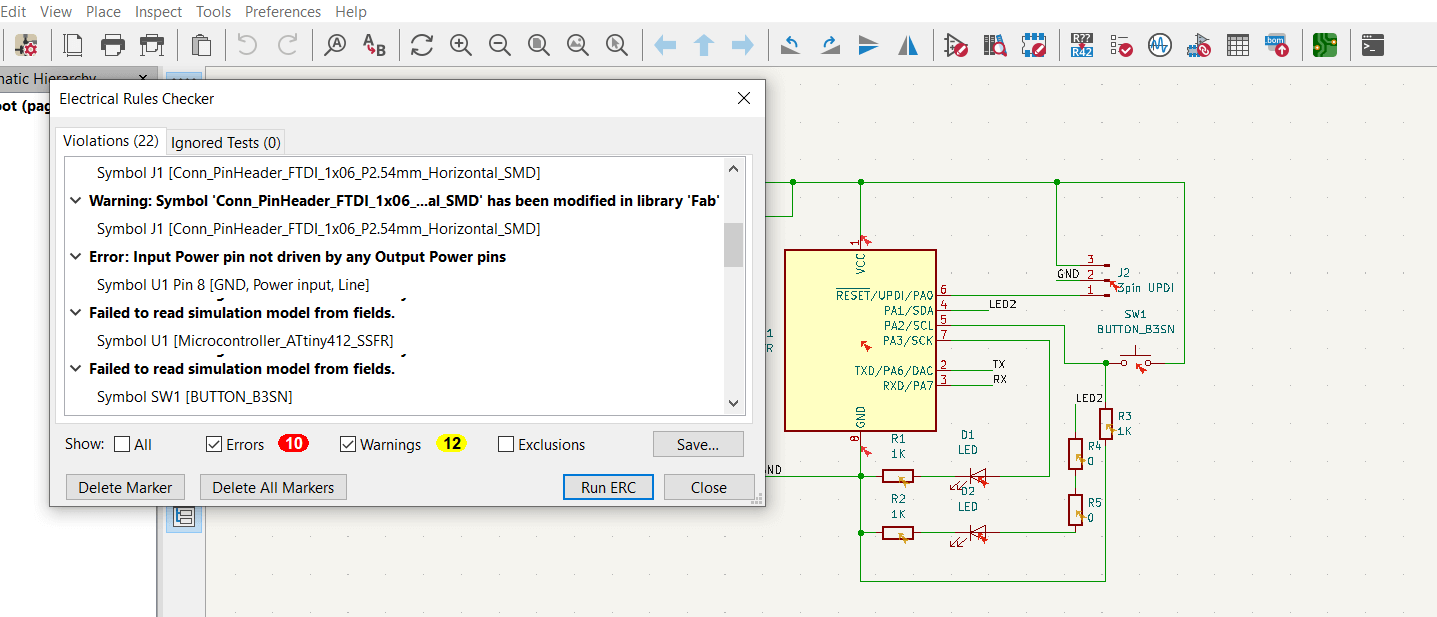
Before moving foward I did the Electrical Rules Check (ERC). I opened Inspect from the main menu tab and selected Electrical Rules Check.
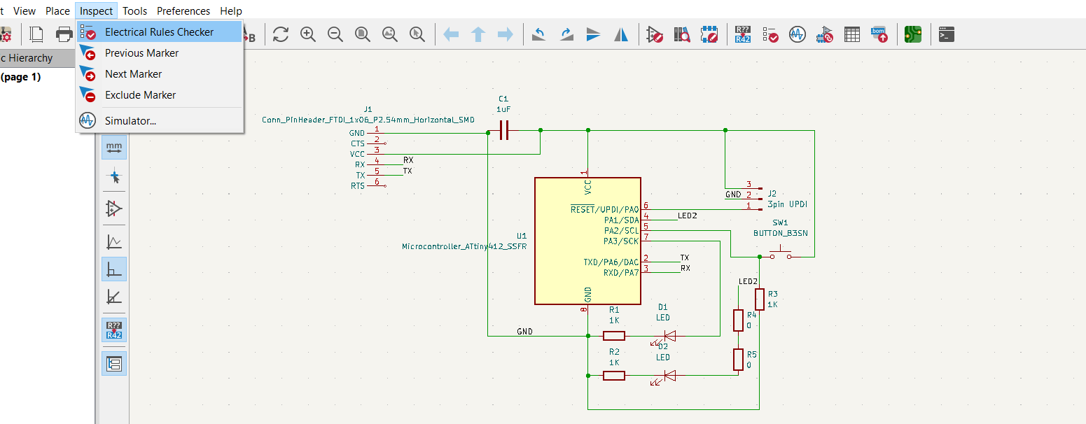
This opened the ERC window and clicked Run ERC. The check returned with multiple errors and warnings, however when I read them, they were associated with the symbols from the Fab library.
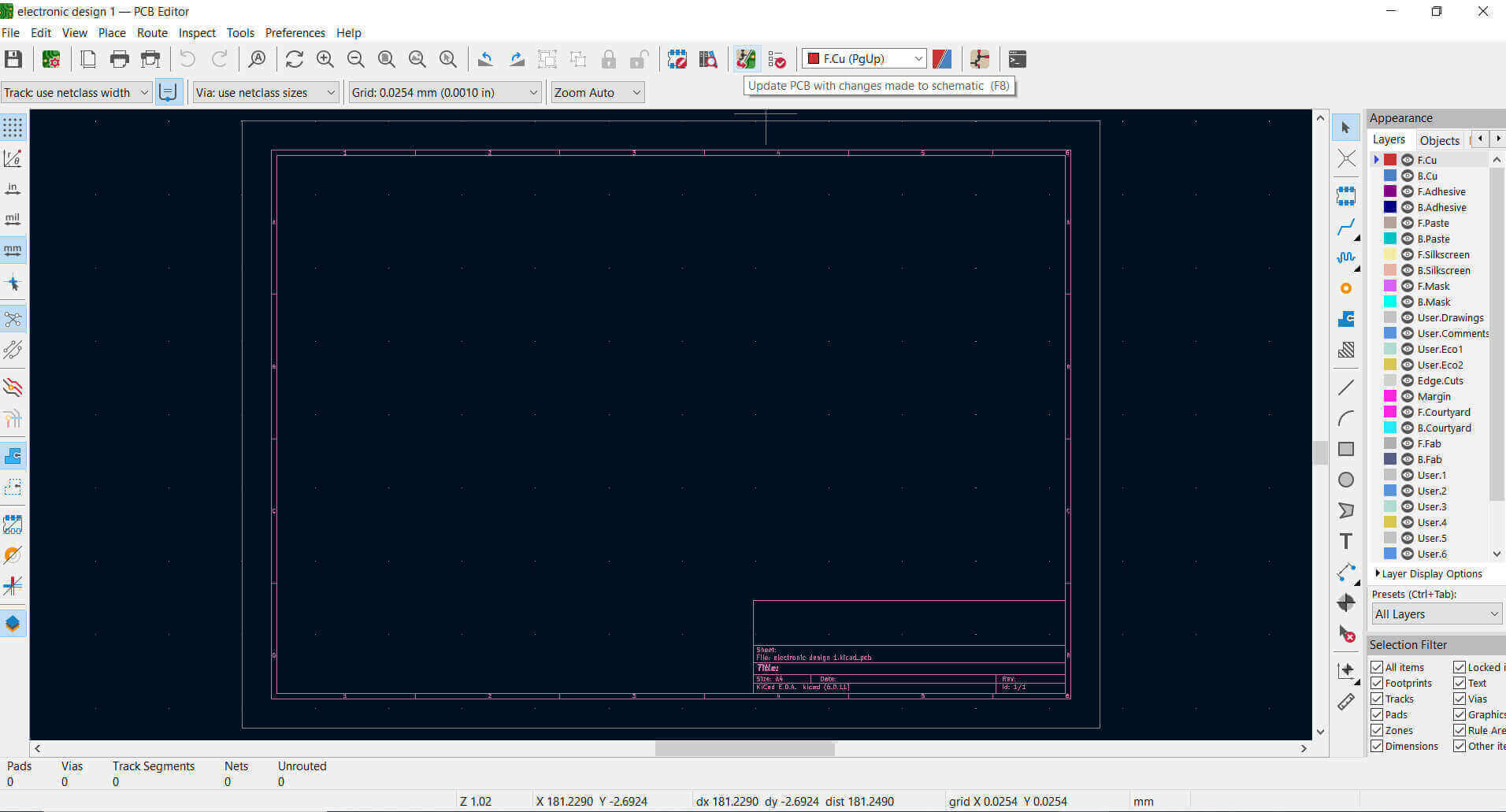
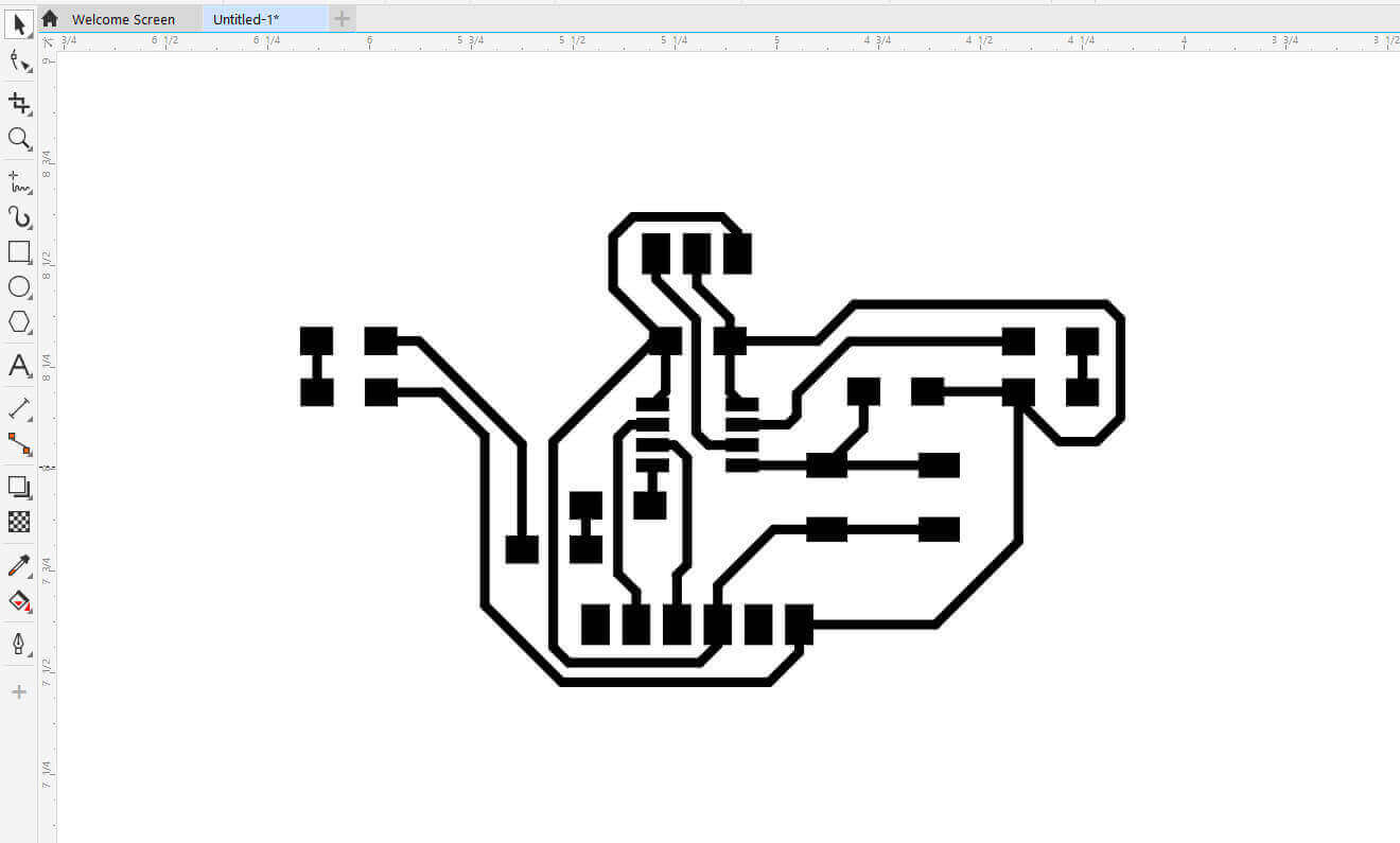
From the Schematic Editor I opened the PCB Editor. I clicked on the Update PCB from Schematic button located at the top.
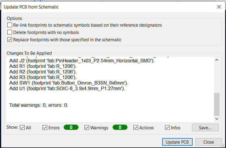
The Update PCB for Schematic window opened displaying all edits made in the Schematic Editor. There were no errors or warnings displayed so I clicked on the Update PCB button at the bottom-right of the window.
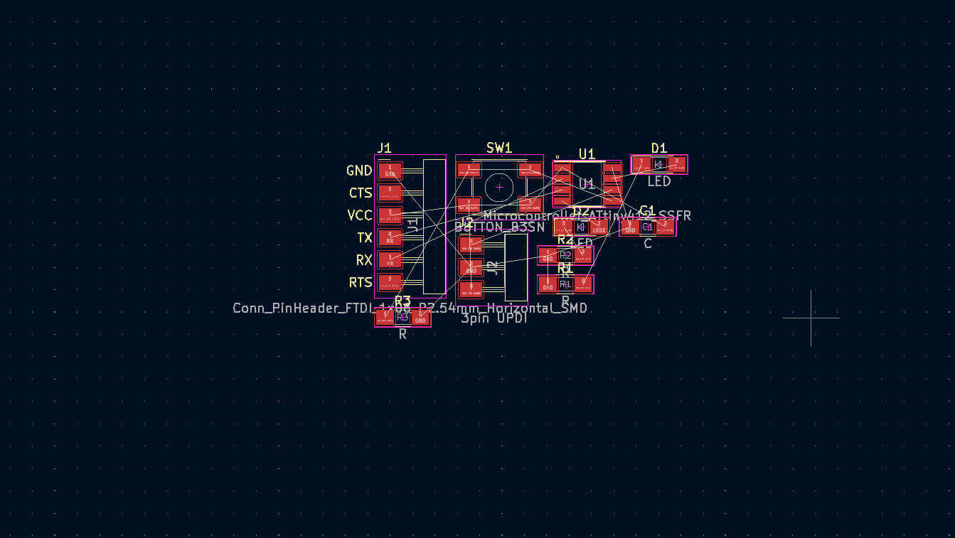
The components appeared in the editor packed together with lines indicating all connections.
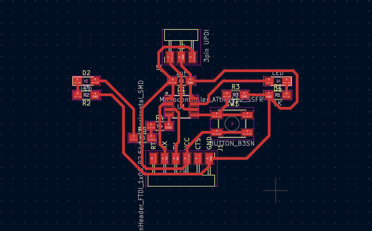
The components were moved into their required positions by selecting the specific component and dragging. To rotate the component, I selected the component and pressed "R" on the keyboard.
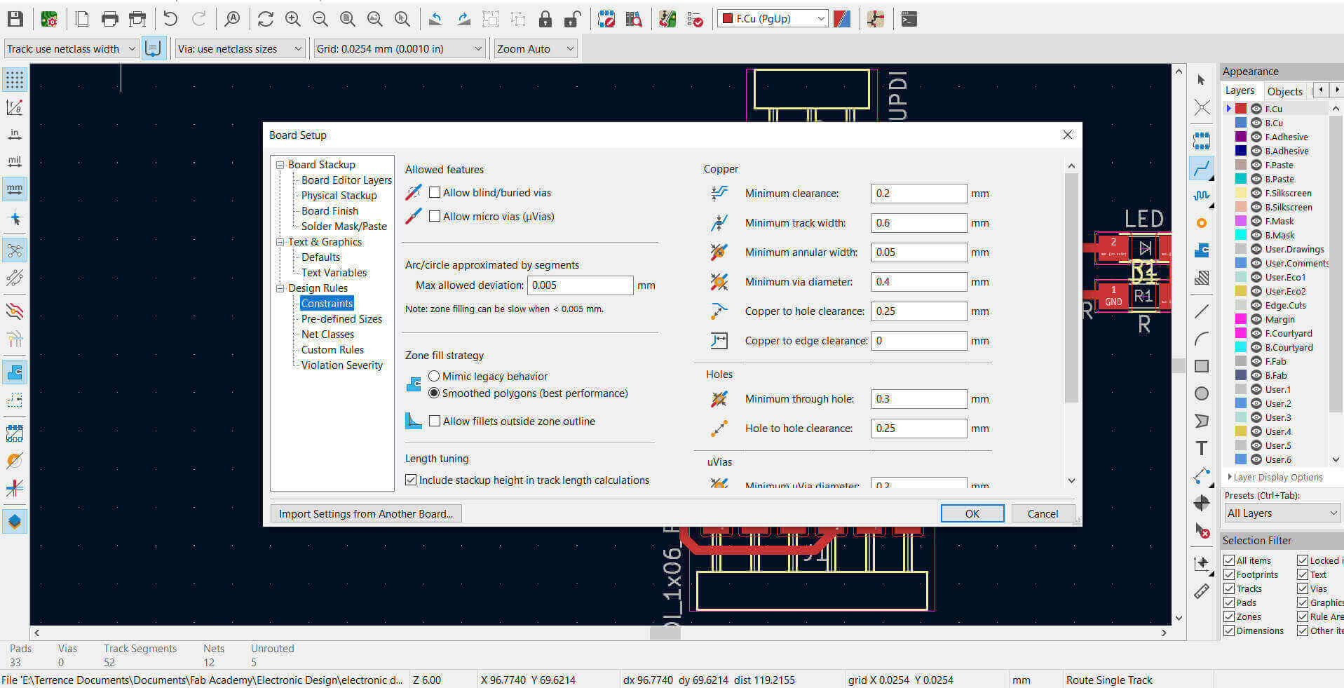
When the components were in the correct positions it was time to draw the line traces to connect them. I needed to set some parameters for this before drawing the lines. To the top left below the Menu Tab there was a tab labeled Track: use netclass width. I click the tab and this opened the Board Setup window. From the list on the left I selected Constraints and under Copper I set Minimum Clearance to 0.2mm and Minimum Track Width to 0.6mm. I left the other parameters at the defaults. I used the Track Tool (the fourth icon downwards on the Tool Panel) to draw the copper tracks connecting the components.
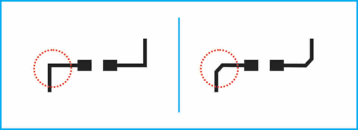
Just a little side note, I realised that when making corners for the copper tracks, it is better to make them at angles about 45 deg. The current flowing through these tracks are similar to that of water flowing through a pipeline. The water at a high pressure meets a very slight resistance at a 90deg angle. Similarly on these copper tracks a high current may cause some heat at the 90 deg corner. This may not be an issue here since this circuit will have a very low current, buts its just "good practice" for when a more complexed circuit with a higher current is being designed.
I placed the components in specific spots and made my connections. I placed the components in these positions because I wanted my circuit board shape to be the Batman logo. The LEDs would be positioned on the wings.
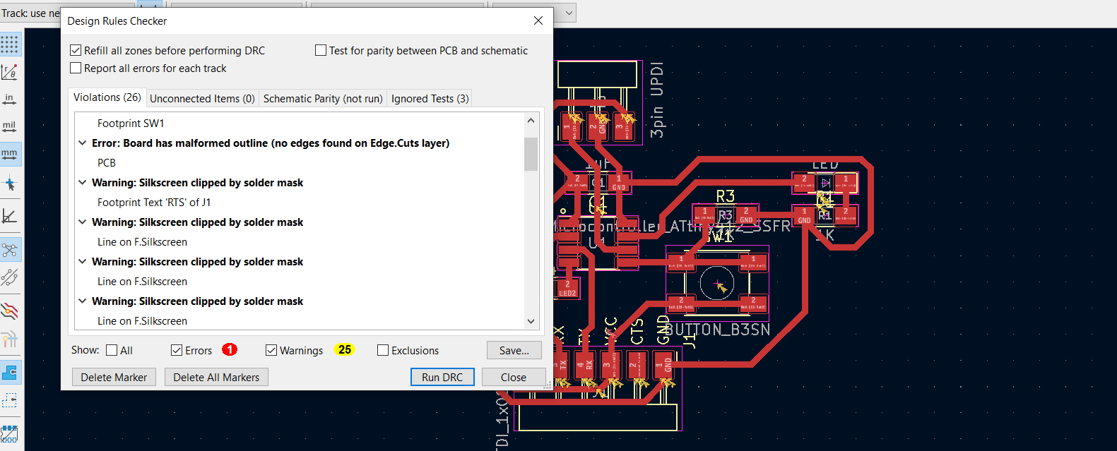
I needed to do a Design Rules Check (DRC) for the layout. From the main menu tab at the top I opened the drop down menu for Inspect and I selected Design Rules Check.
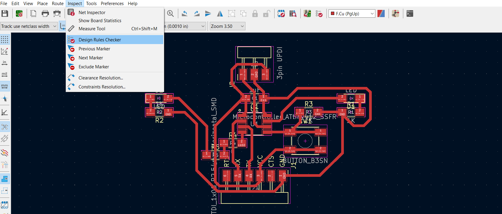
The DRC window open and I clicked Run DRC. One error came up which indicated that I didn't have an outline. This wasn't a major issue because I didn't put an outline on purpose. I wanted to design a customized outline to match the shape of my board which I used CorelDraw.
Multiple warnings came up also, but just like the ERC, they were associated with the footprint designs from the Fab library.
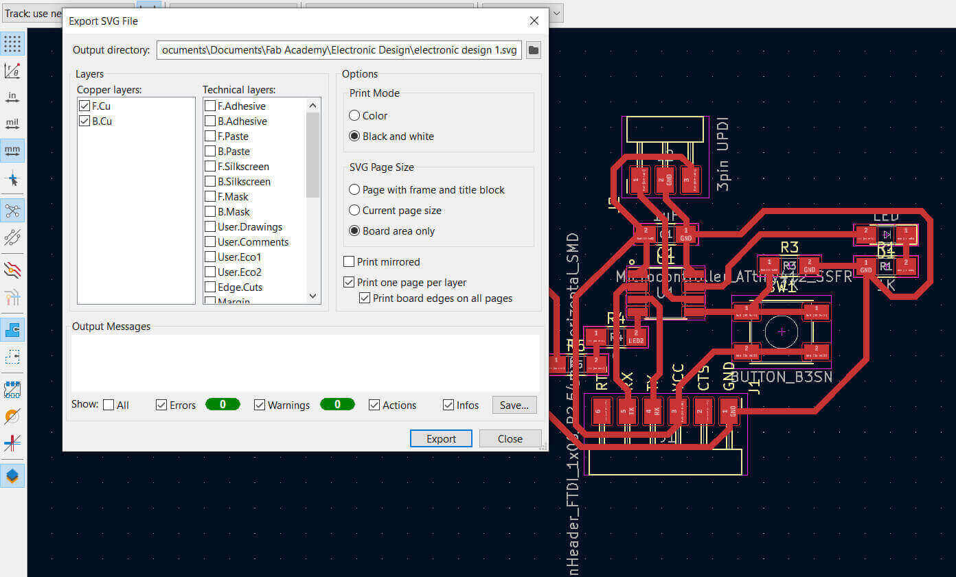
I then exported the final design layout as a .svg file.
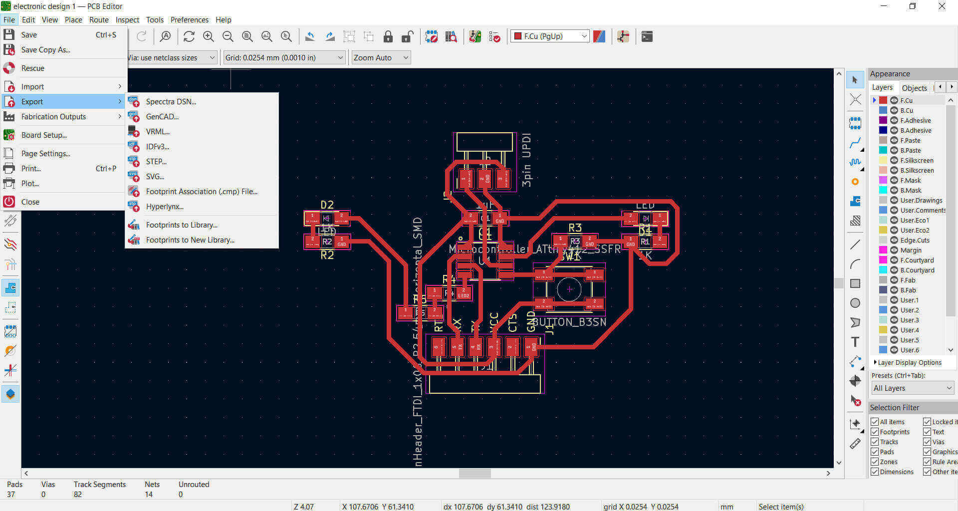
The Export SVG File window opened where under Copper Layers I checked F.Cu and B.Cu and Print Mode set to Black and White.
I imported the .svg file into CorelDraw where I drew the Batman logo. I placed the circuit inside of the logo and I added a border which highlights the shape and also serves as a ground.
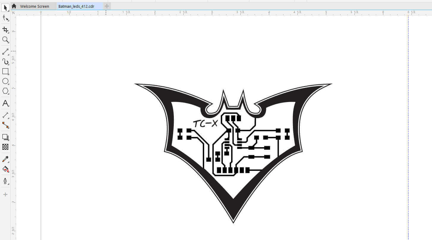
For the milling process I will be using a .png image to send to mill. Since my image is black and white, when prepped for milling whatever is black will be removed. The actual copper traces are in black and will be removed but this is not what I want. So to fix this I inverted the colours of the image in CorelDraw which switches black to white and vice versa.

My circuit design is completed and ready to be produced. See Electronics Production for completed circuit.