5. Electronics production
For this week, I have learnt on:
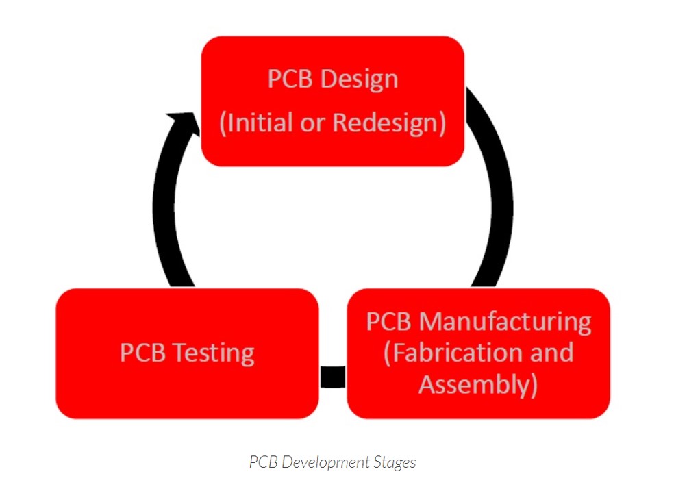
How to build a Printed Circuit Board, PCB, by:

1. Lithography?
-
Types of Circuit Board
-
Multi-Layer Board Fabrication
-
Image Expose & Develop
-
Automatic Optical Inspection
-
The Production process after Lamination of Multiple-Layer Panels:
-
Primary or First Drill
-
Deburr
-
Desmear (Multi-Layer Board Only)
-
Electroless Copper Deposition
-
Dry-Film Resist Coating, Expose & Develop for Outer Layers Panels
-
Copper Plating for specific pattern
-
Tin Plating
-
Dry Film Resist Stripping
-
Copper Etching
-
Tin Stripping
-
Exposed Surface Cleaning and Free of Oxidation
-
LPI Solder Mask Application
-
Solder Mask Curing
-
Ink Silkscreening (Legend, Nomenclature,Component Designer)
-
Hot Air Solder Leveling
-
Routing or Fabrication, Line Scoring
-
Bare Board Electrical Test
-
Final Inspection
2. Machining
-
Removing the Finger Oil from board
-
Replacing Endmill
-
using FabModules
-
Sending the job and Milling Traces
-
Checking of Traces Quality
-
Placing the 1/32” endmill at origin
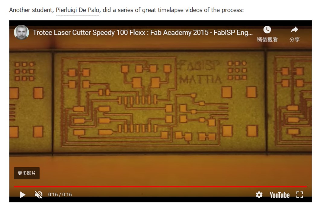
3. Vinyl cutter

4. Laser cutter
5. Printing
6. Electroplating
7. Sewing

Before this lecture, I cannot imagine that electronics production can be applied to the sewing industry. This arouses my interest to design my own PCB for my final project about Automatic AquaPonic System.
For this week, I worked on:
Group Assignment
We have characterized the design rules for our PCB production process. If you have interest, you can CLICK HERE to know more about the details.
Individual Assignment
Our PCB Production Process
We all grouped together to characterize the design rules for our PCB production on digital way by using CNC machine after the lecture. One of my experienced teachers and one of my graduated students as the guest insstructor introduced this machine for us. They also shared his teaching experience on traditional way by using chemicals. After our discussion, our design rules are as below:
Preliminary Work
I had to download the open source for the png file of FabTinISP Minimal which was used for milling. Therefore, that I had found this png file from Brian website which was provided by Behnaz Norouzi.

I have used fabmodules to generate the png file from G code from the website. We can insert png file and choose the categories of othermill (NC) and process (PCB traces 1/64). Then, the button (calculate) was pressed.

I also choose the tool diameter as 0.1mm which was fit for this milling. G code was generated for milling. Number of offsets was set as 4 which made sure the thickness of traces was enough.

STEP 1
Checking on the operation of CNC Milling Machine Roland MDX-500

- During checking process, the first trial of milling PCB is unsuccessful because the level of the circuit board was one of the successful factors. I have found that adjustment and balancing were necessary.

- Therefore, a flat wooden platform was prepared for milling of this PCB and made sure that the PCB was balance.

STEP 2
Preparation of all materials used - Printed Circuit Board without Traces (material is FR-1 that is suitable for DIY Milling Prototype)

STEP 3
using Fab modules by computer Before Milling (Starting from index.html)
-
Downloading the PNG files for the traces and the board outline
-
Generation of G-code for programming

-
Transferring G-code to the CNC milling machine

STEP 4 Milling
-
Setting Bench mark for different Curving V-Bits
-
Curving V-Bits “3.17510deg0.2mm” (Left Hand Side)
-
Curving V-Bits “3.17510deg0.1mm” (Right Hand Side)
-

-
Choosing engraving tool used which is “3.17510deg0.1mm”(Right hand side)

-
Trials using different offsets

- Panel for manual operation and setup

- Setting Work Origin by changing G-code

- Placing the selected Work Origin

- Using Vacuum Cleaner to Remove Fragment

- Trial Product of (Left-hand Side) & Finished Product of PCB (Right-hand Side) and Using Sand Paper for Removing Extra Copper from board

- Finished Product of PCB

STEP 5 Soldering
- Preparation of all materials used - Sample Book for SMD Resistors and capacitors

- Preparation of Materials used :Resistors, Capacitors, Zener diode, ATtiny 85, PCB, 6-pin Jumper, 2 LEDs

-
schematics of the FabTinyISP

- Resistors used

- Soldering Iron

- Cleaning for Soldering iron tip to make sure that no any impurity attached on the surface.

-
Soldering Resistor as an example on PCB

-
Soldering all components on PCB. This is my first time to solder and learn some tips :
- Our soldering iron is used for long time and not sensitive during soldering. We must press Tin metal on the surface of PCB for few more seconds.
- Forceps are used to hold resistors more stable to make sure solder them on the right position.
- Soldering Tin metal must be done part by part to make sure the appropriate connection and not short circuit.
-
Surface of resistors with value (i.e. 1001 = 1000 ohm) must be faced upward or Zener diode must be determined their polarity.
-
Brainded Copper Wire for Residue Aborption

-
Completed FabTinyISP vs PCB

STEP 6 Board Electrical Test
STEP 7 Debugging
-
3 Types of OS operation: Windows, MacOS, LINUX
-
LINIX is highly recommended because of compatibility
-
LINIX can be acted as the role of a book.

- ArduinoISP V2 can be acted as the role of a teacher who have read a lot of books and taught students to learn.

- FabTinyISP can be acted as a student have learnt the programmed from a teacher.

STEP 8 Burning Boot Loader
-
Burning the firmware to the FabTinyISP

- According to instruction after checking, Blow the Reset Fuse

STEP 9 Test on the in-circuit programmer
- Changing value (i.e. delay(100) to delay(10)) to have the different frequency of light flashing.

STEP 10 Final Inspection
- Except FabTinyISP, ATtiny85 can be applied to other based Target board
Individual Assignment
Studying all the the useful references for the design rules for my PCB production
- What is PCB Fabrication Process?
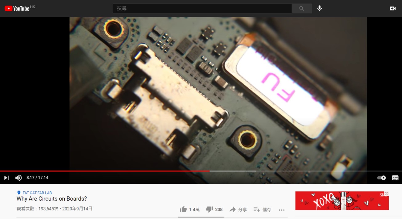
- Why are Circuit on Boards?
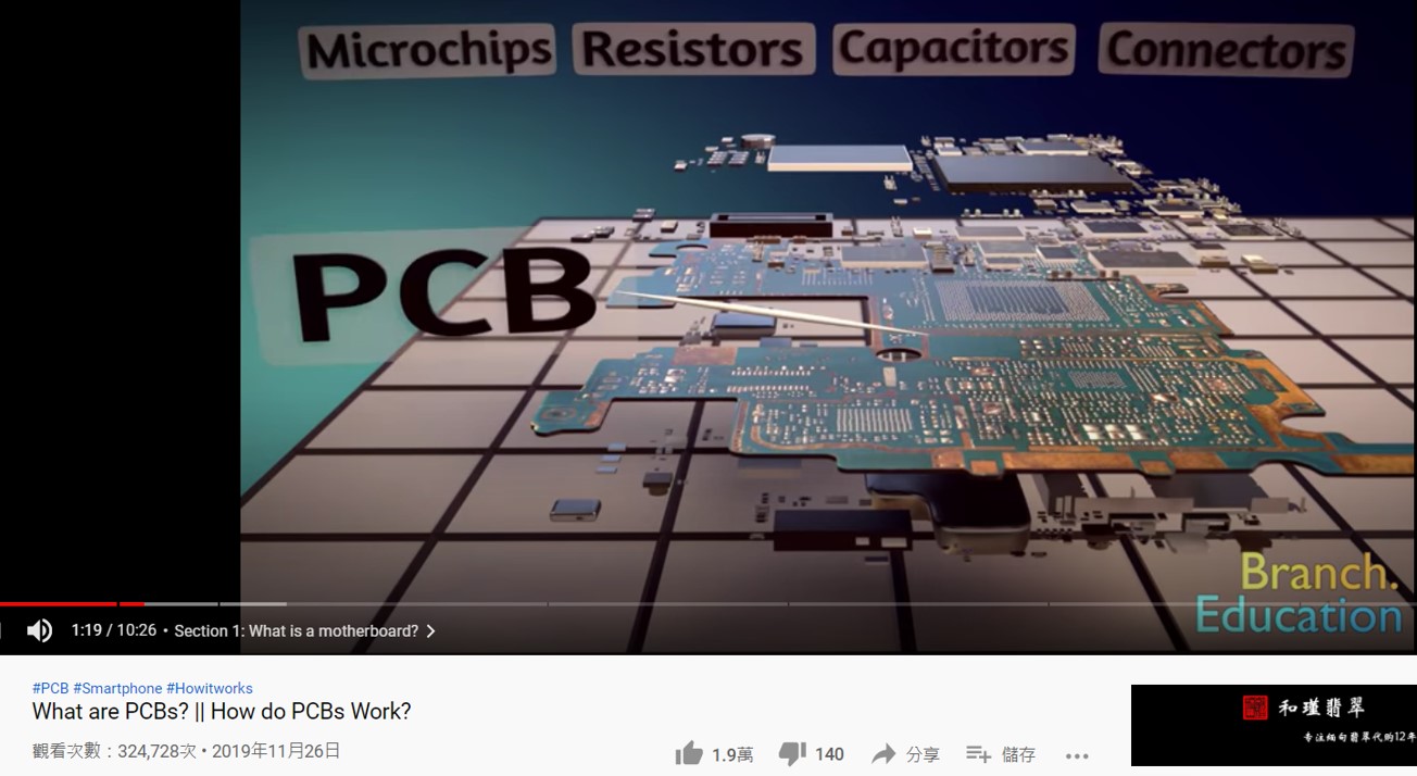
- How do PCB works?
After this week, although I still have much challenge that should be faced, I have much more confidence to make an in-circuit programmer which can be applied to my Final Project, Automatic AquaPonic System, as following the above design rules in the following weeks:
If you can’t explain it simply,
you don’t understand it well enough.
Albert Einstein