Electronic Design
PCB design
I must say that it has been a long journey to get to the design of the electronic board. I have designed several, but they were unsuccessful in soldering because the components were other. Finally I was able to have the final board with the right components. I will use this board in my final project.
I chose Easyeda for the Great Liberia that has connected to the LSCS Parts store. It allows you to design your schematic diagram, design your traces, have a 2D and 3D preview of your PCB, see your parts, take an estimated price from your components. I think it's an efficient online software.
During electronic production's week, as a team we had explored a bit on the course with the Hayashi guide, we learned how to make a schematic small of a circuit with a resistance and a LED, such as the example of the class. This week of electronic design we applied again what we learned, but then we developed more in Eagle.

One led exercise
To use EASYEDA you must first create a user. And then you must enter the button that says EASYEDA Designer. And ready, you can always enter from your browser with your user.
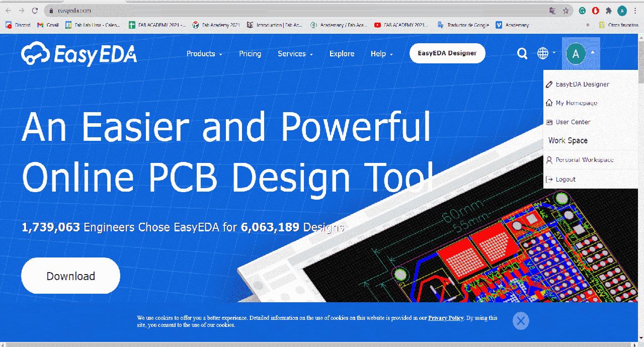
EasyEda site
Week 6 Assignment
GroupTask
To develop this week we met in the laboratory to do the group part, in general terms we tried to do it. With a little more time at home I was able to use the oscilloscope in a calmer way and I was able to test my ISP board.
Check the Design Rules
In this challenge, the collaboration of Hayashi y Mayra with whom we learned enough about many concepts of electronics was very important.They also documented the group exercise in their pages. For example, we saw the formulas of how to calculate the proper homage of the resistance we will use in the circuits we will design.
The words we got used during this week is:
| Ohm | Voltage-5V | Sources | Resistances |
| Switch | Positive | Negative | Circuit |
| Traces | Components | Ground | VCC |
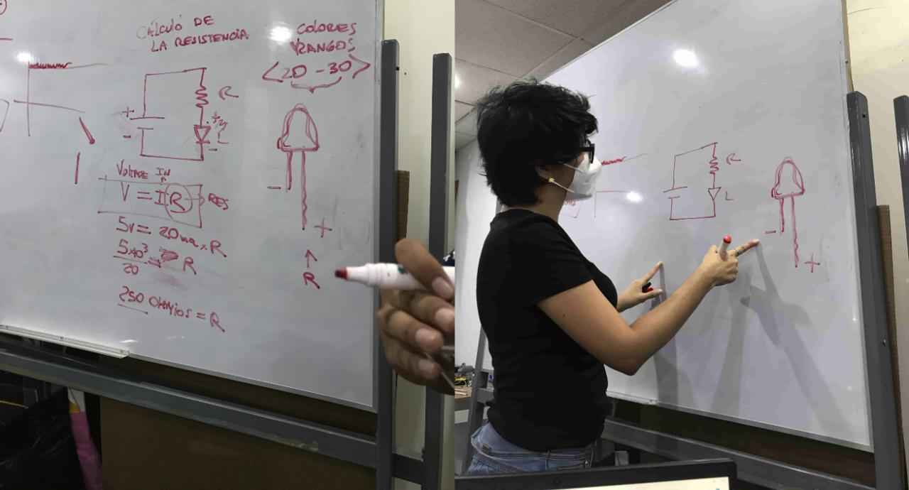
Studying electronics
Testing with Oscilloscope
The first step to test my isp board with the oscilloscope is to load a small program to my board, I made the led of the board light up increasing the intensity of the light so that the oscilloscope can measure a signal that varies.
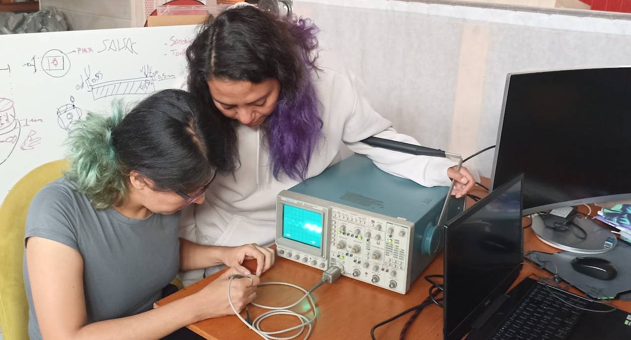
Playing with the oscilloscope
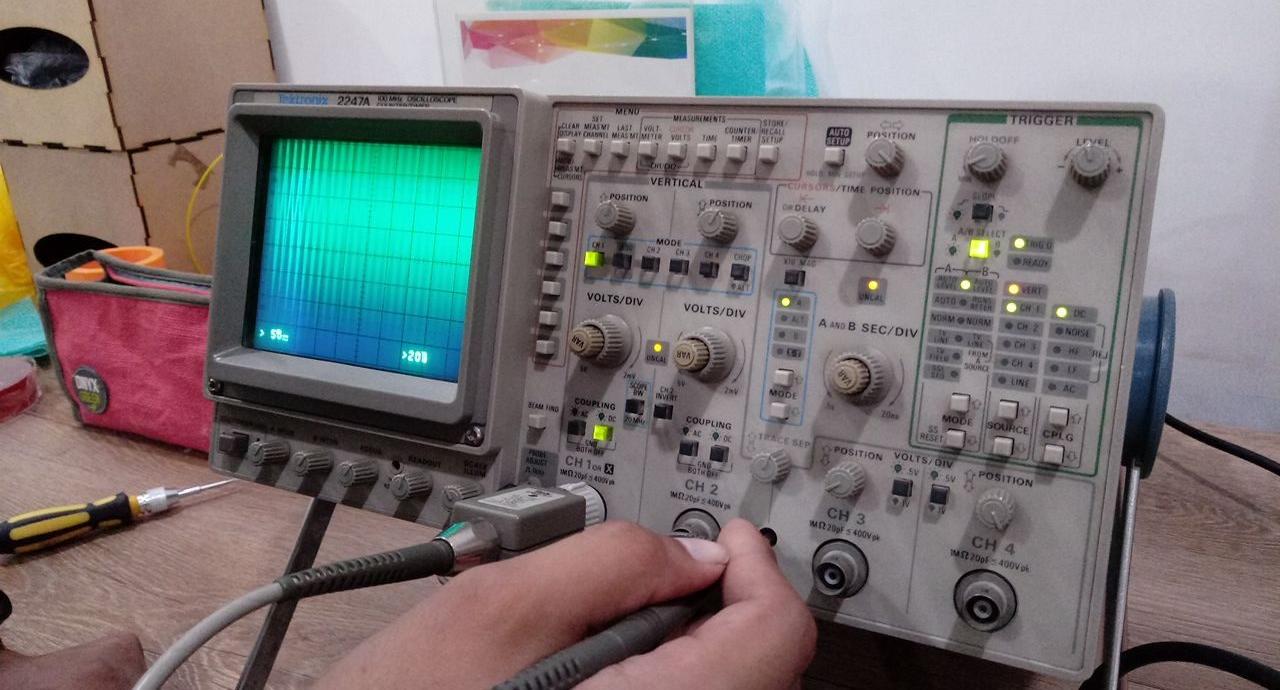
Oscilloscope of 1970 🧐
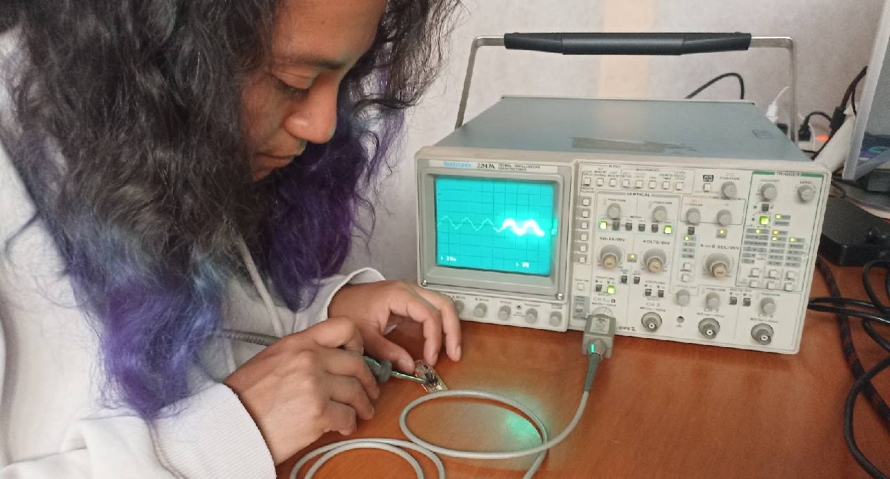
Testing the signal only
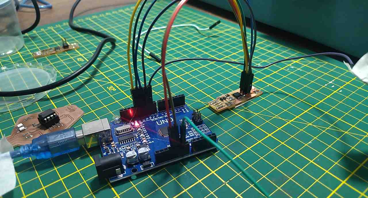
Sequence 1

Sequence 2
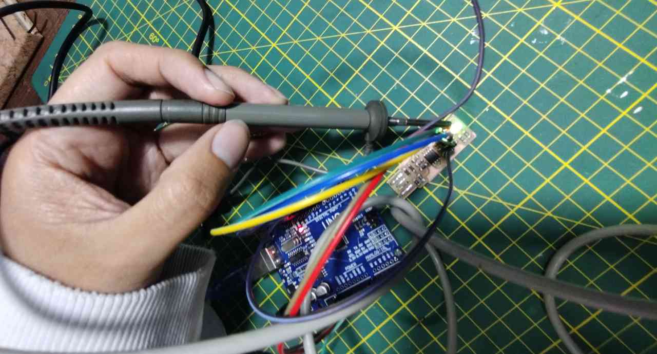
Sequence 3
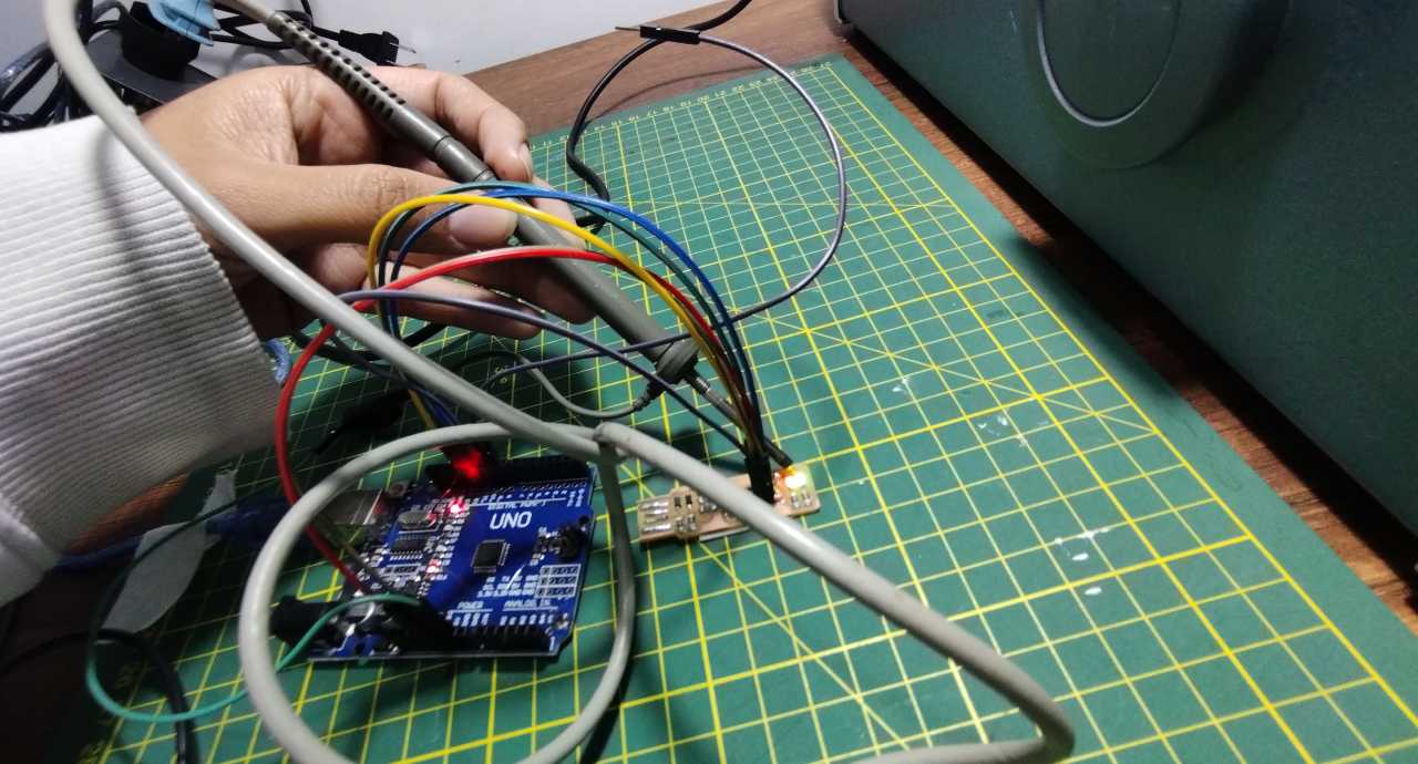
Sequence 4
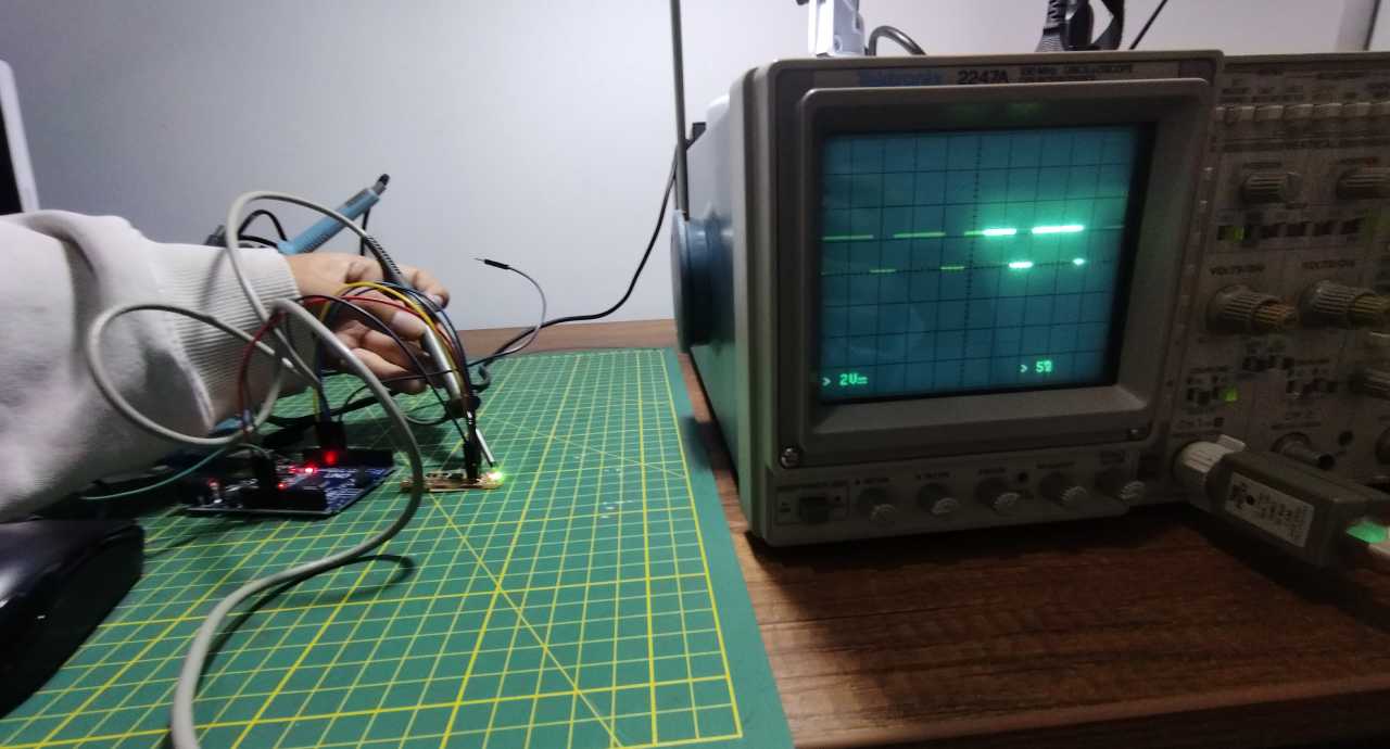
Positive side of the LED
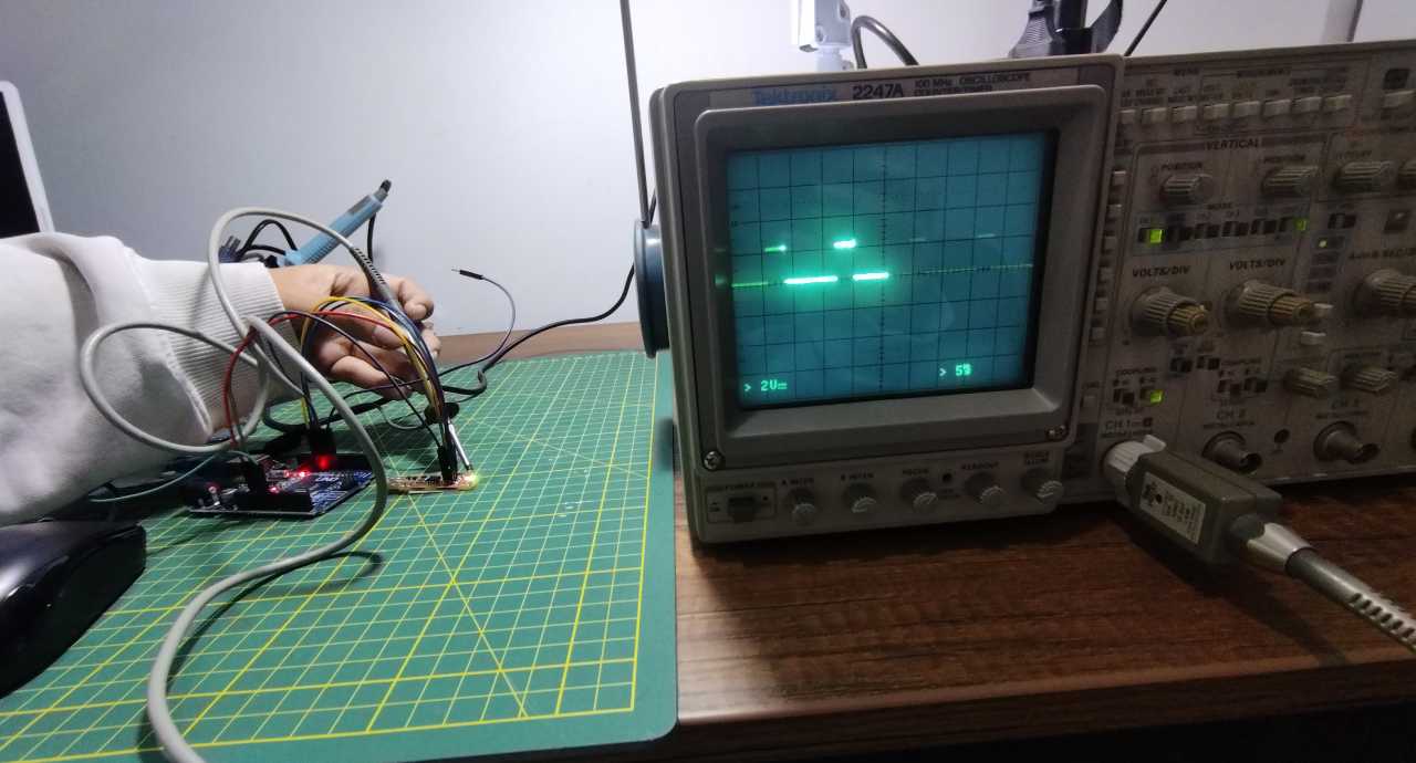
Positive side of the LED
Testing with the oscilloscope the led sequence
IndividualTask
First, I had to understand what I needed for my PCB. In my case, it is a programmable board with a USB output and an I2C output that will help me display on a small LED screen. It also has a push button switch and a programmable LED. I tried this design with Hayashi's help, the idea is to make a practice for my final project.
Steps to make my board
- Imagine the components I will use
- Design the schematic of the circuit
- Then cook the PCB, modify the traces and the shape of my plate.
- Expor said design in Gerber format.
- Import said format in the Flatcam development software.
- And finally import it to the software that will allow us to mill in Modelite.
- * Note: Modeling, it is a dear CNC Router to mill our boards
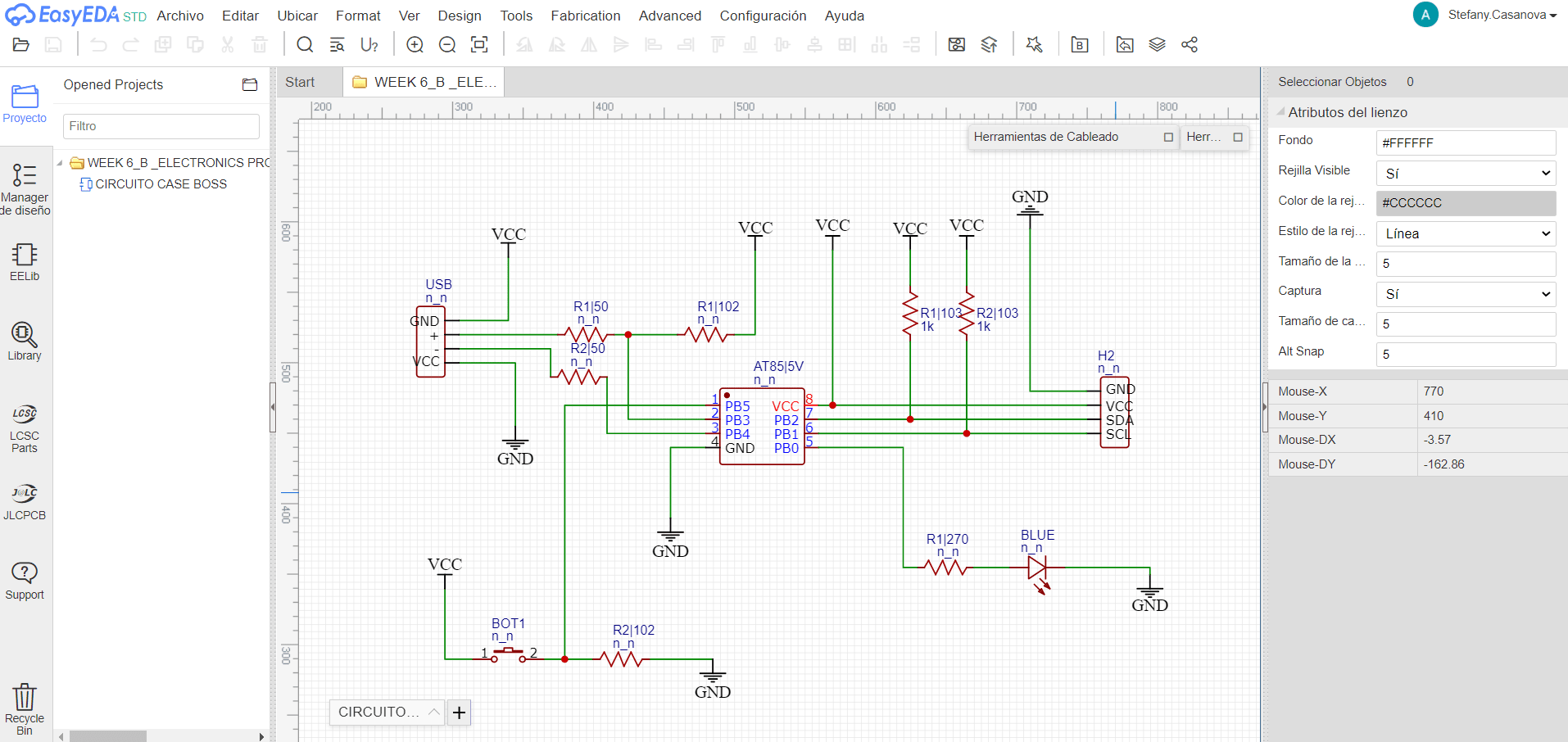
This is my schematic drawn in EasyEda
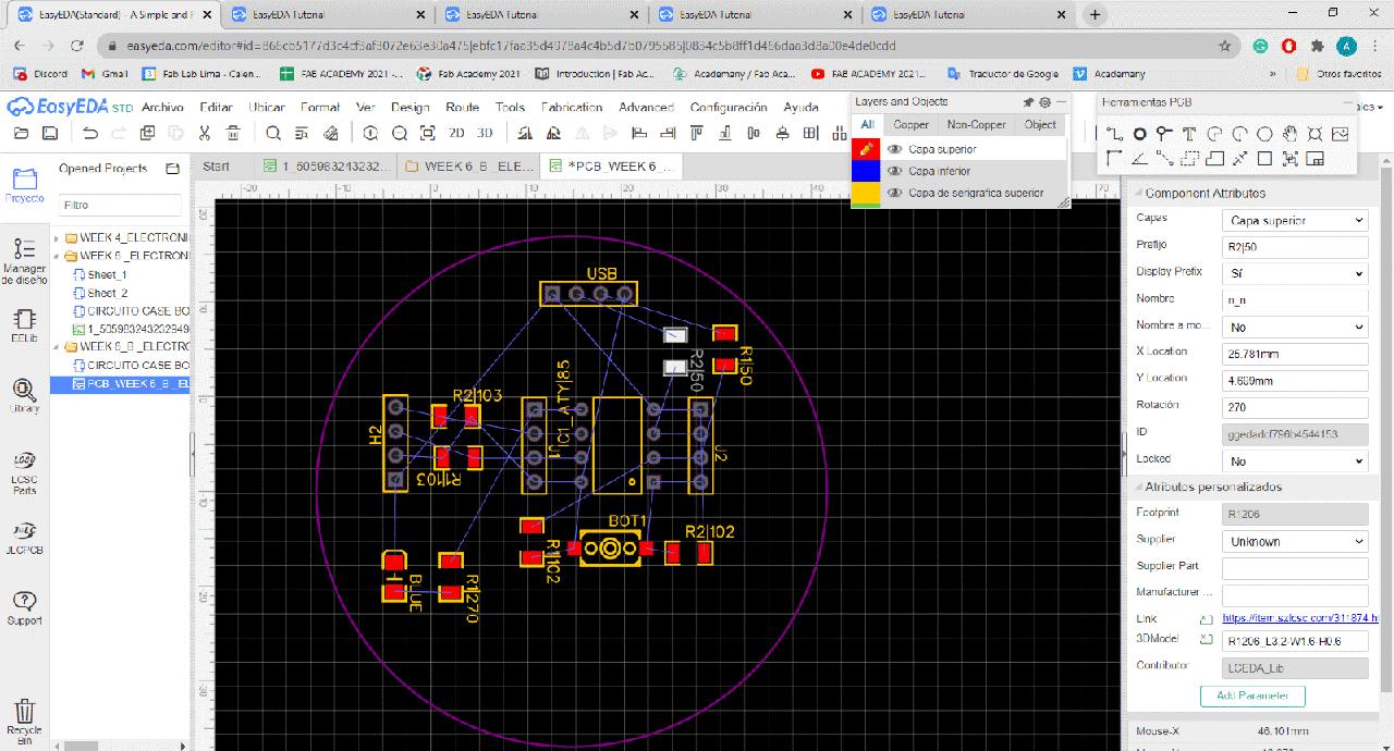
Placing components
Then I developed my PCB and tried to arrange my components so that the EasyEda autorouter would simplify my life and help me to design the traces in a preliminary way, but that never happened. but that never happened, for a long time, the only thing I saw was:
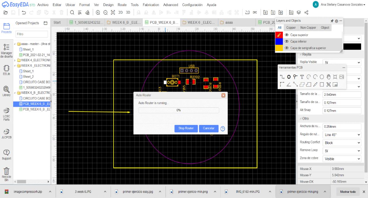
Auto Router for traces
Then I wanted to propose my own style of traces and I vectorized an image of a very curious paracas deity, because it seems to be an electronic board with USB output.
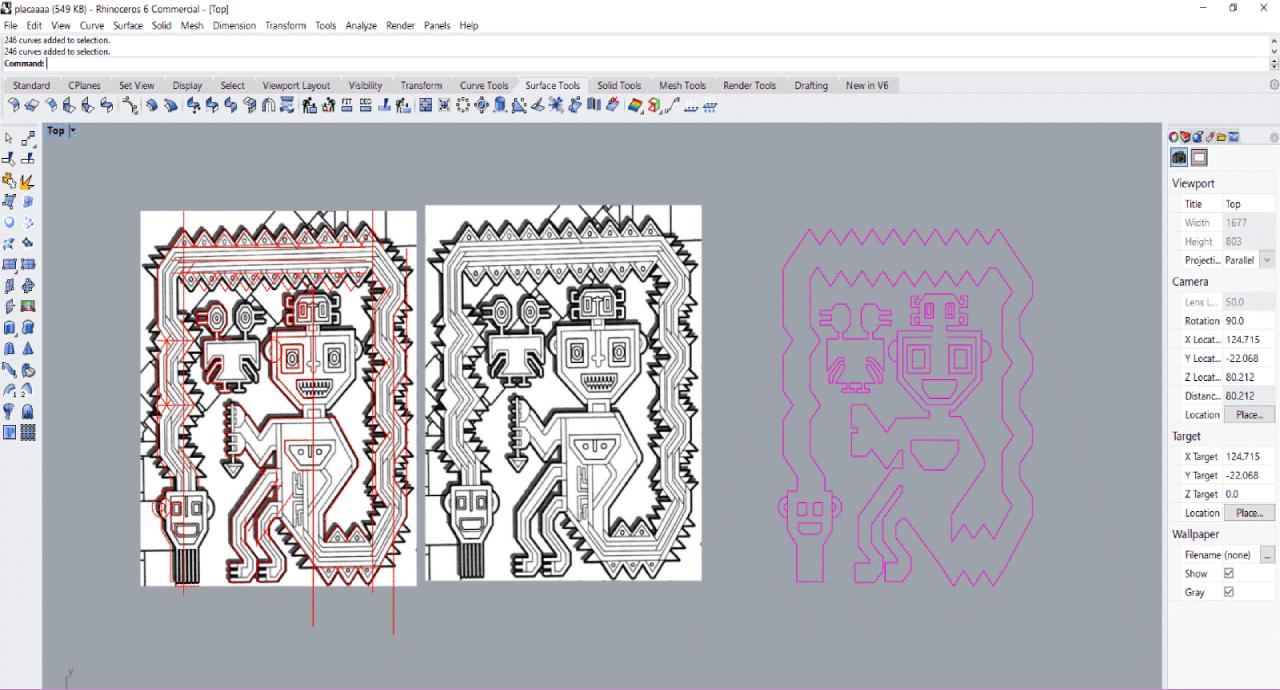
Drawing the cutting line
Now I'm trying to convert these vectors in traces, to connect my components
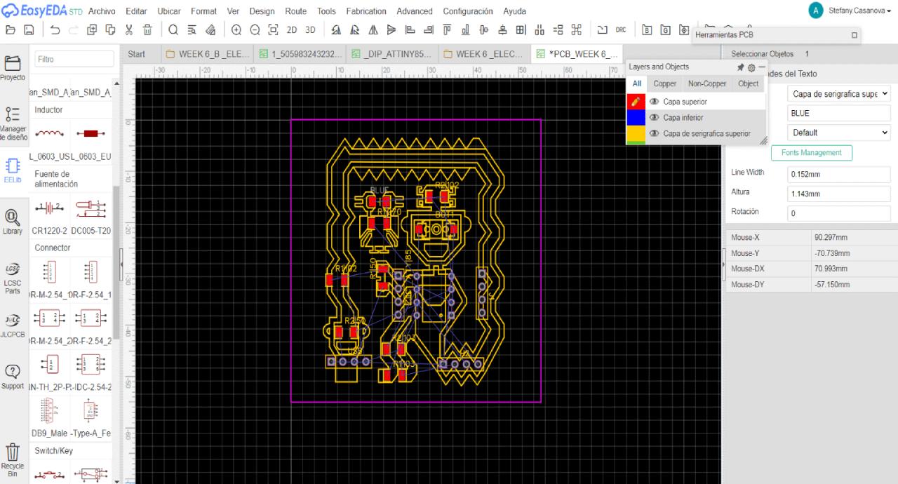
Import the vector
It is very fun as seen and fits, but it is harder than I expected, trying to understand the logic of the circuit I realize that between the schematic and the design of the PCB there are several factors that take into account to accommodate our components, such as: The proximity of the resistance to the components that are affecting.
That the output components are not in the center to be easily "connected" instead, in schematic you can place it anywhere in the sheet if you wish. It is important to maintain an order of the components, in the two work spaces, both in schematic sheet and, in the PCB lamina, to quickly identify what is being worked.
Second Design
I surrendered up with the first design because it can't solve the traces, so I decided to make a second design and I was inspired by the locomotion logo and also designed it in EasyEda.
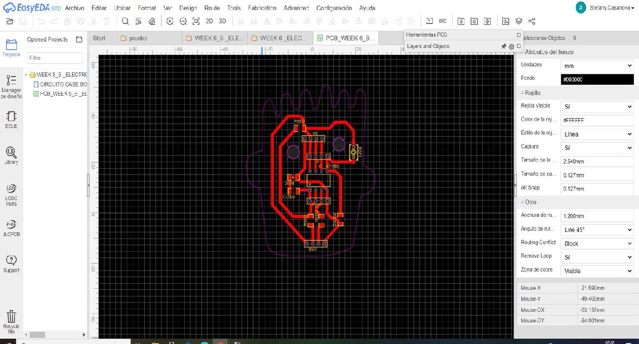
Design in EsasyEda
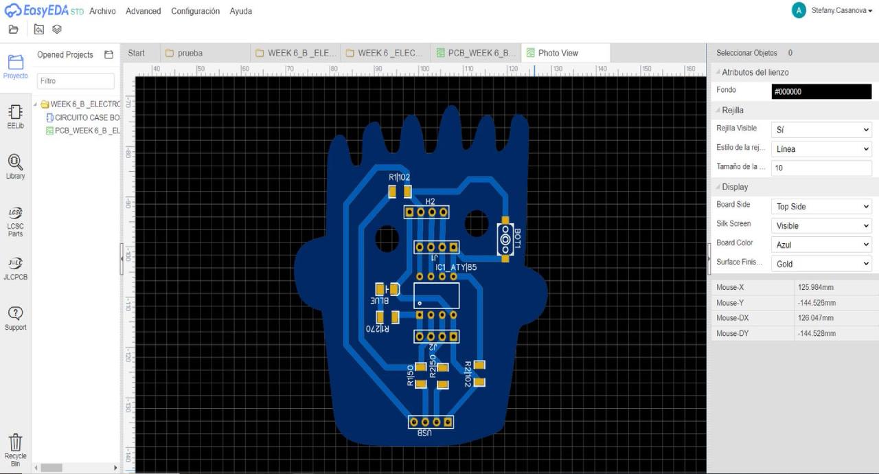
Design of Locomotion pcb 2
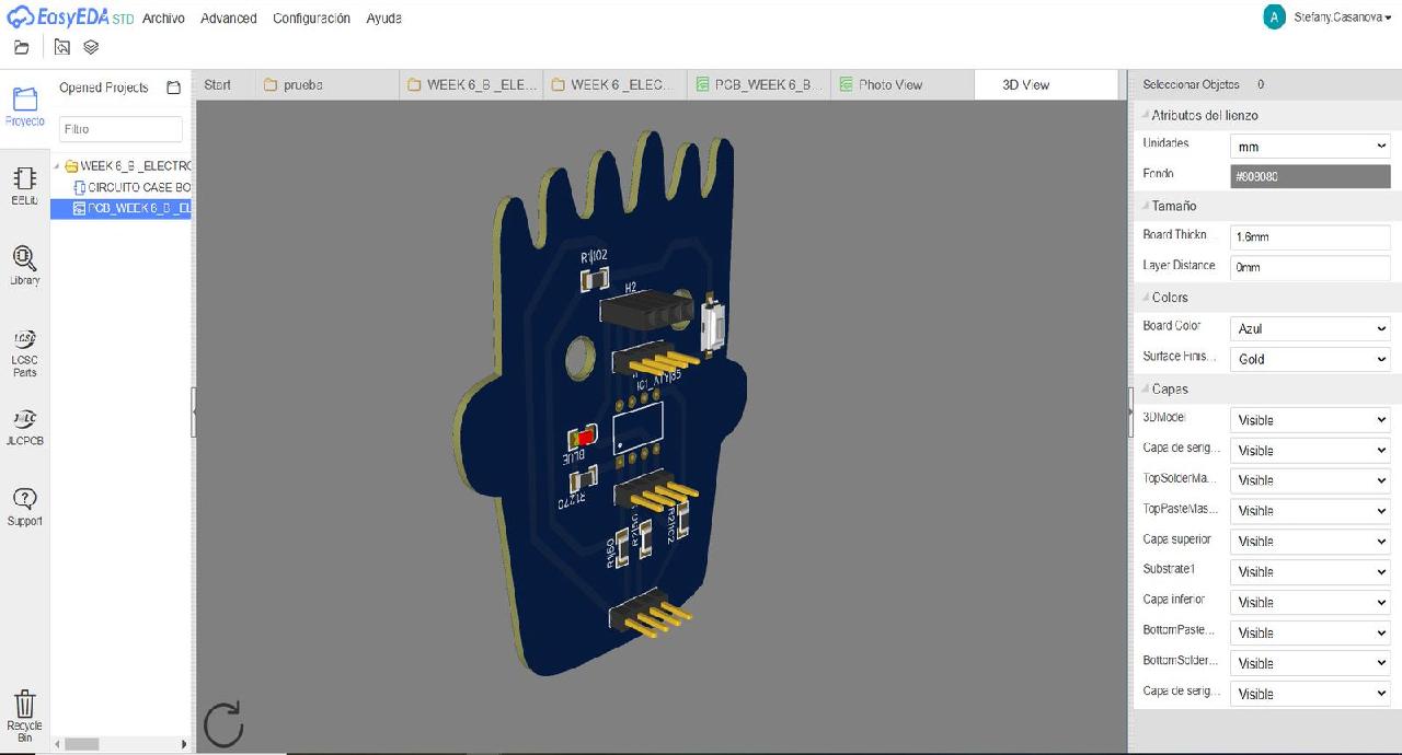
Design of Locomotion pcb 3
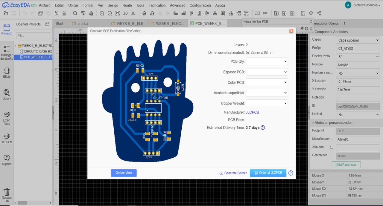
Generate gerber
After finishing the design we took it to the Flatcam program to process it and generate the trace file and the outer edge. In Flatcam we set the depth of cut, milling diameter, number of passes and export the format to G-code to be read by the CNCjs program.

Flatcam Work sequence 1
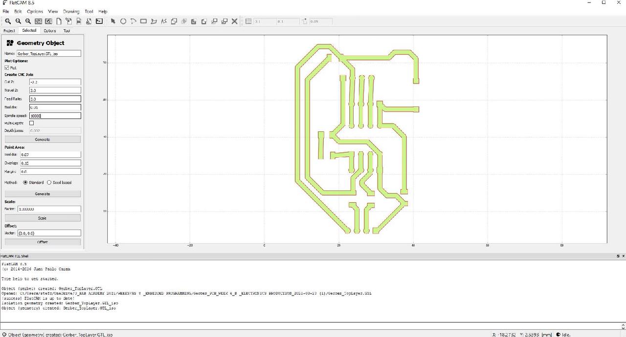
Work sequence 2
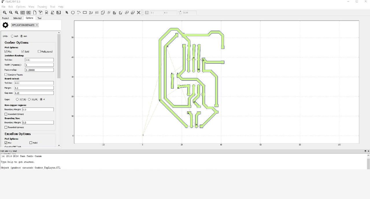
Work sequence 3
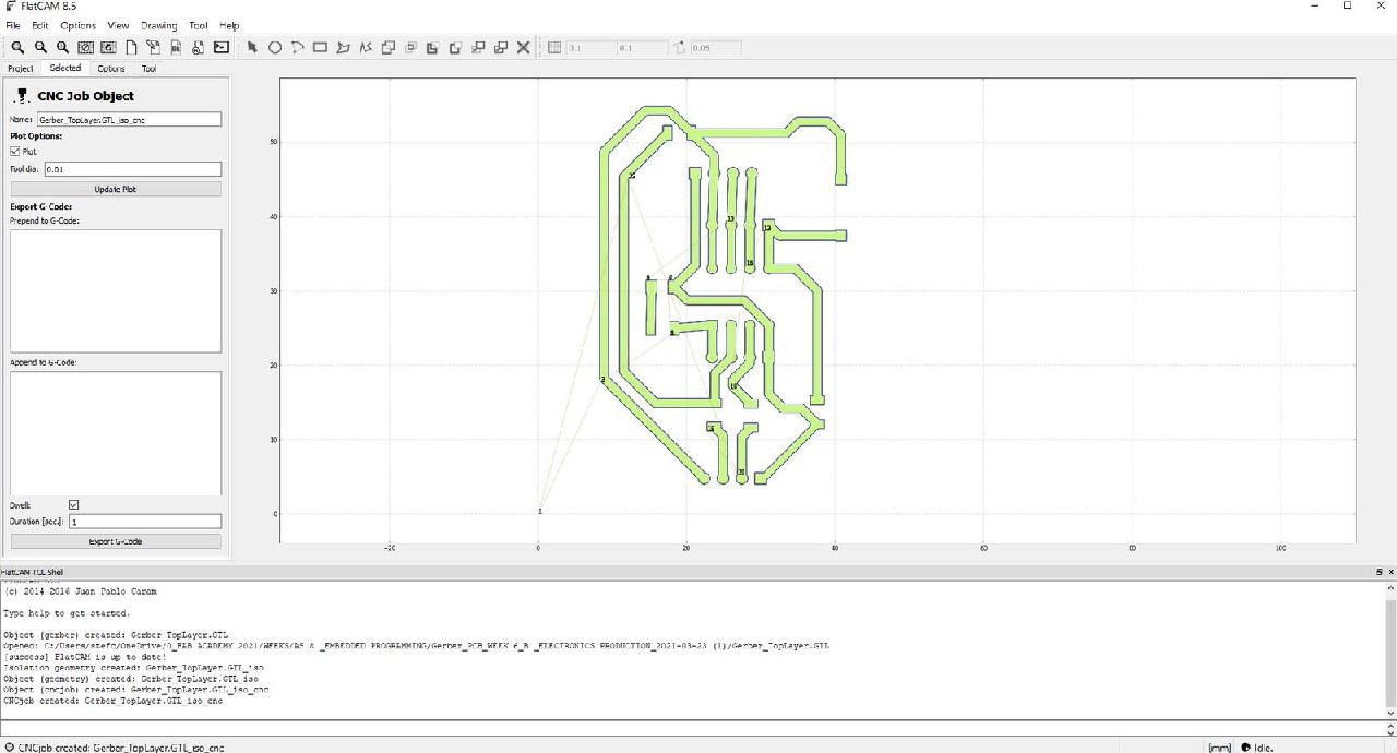
Work sequence 4
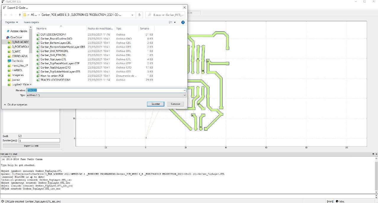
Work sequence 5
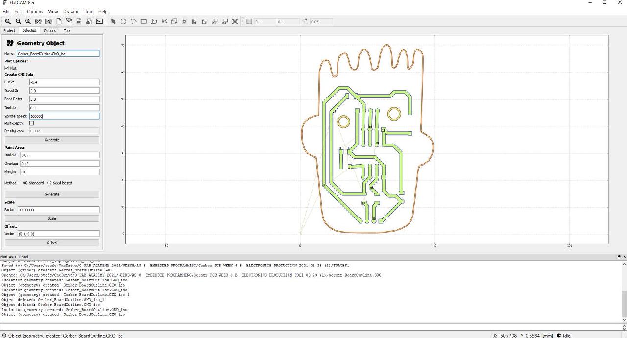
Work sequence 6
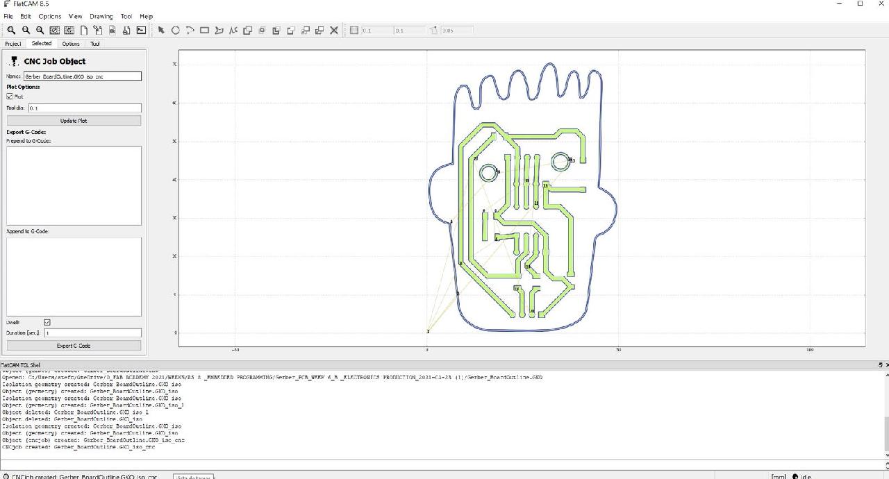
Work sequence 7
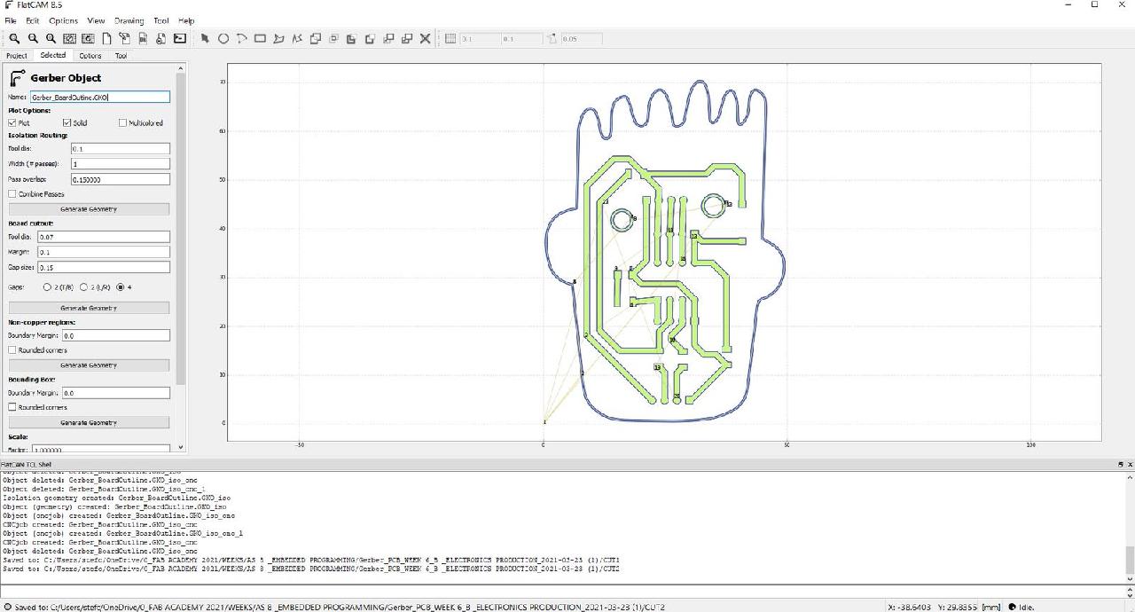
Work sequence 8
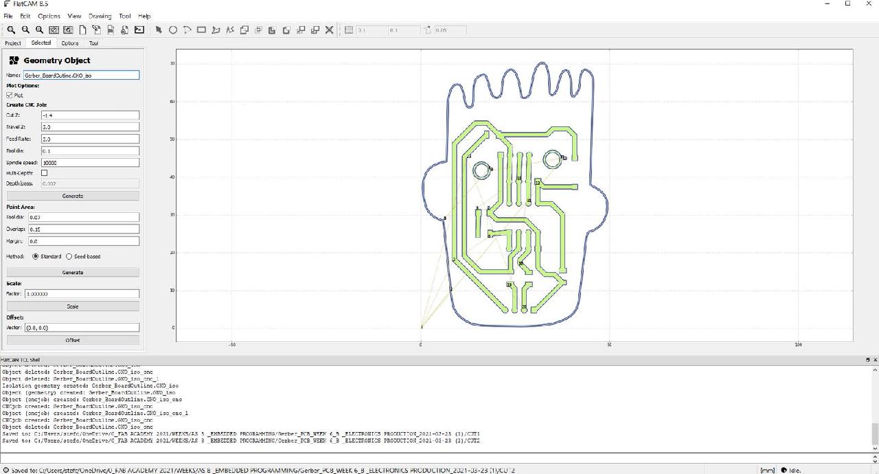
Work sequence 9
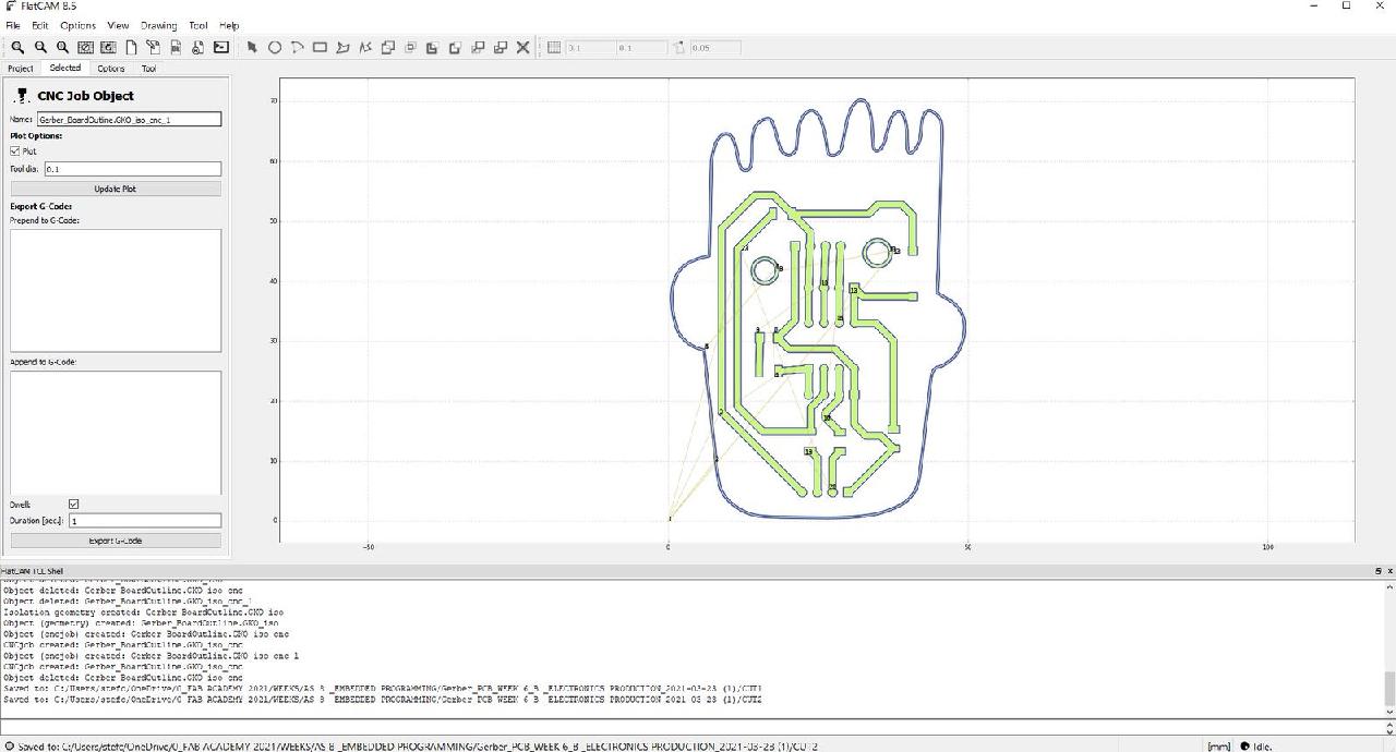
Work sequence 10
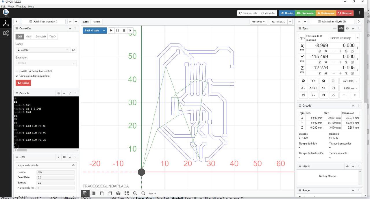
G-code CNCjs
I then proceeded to mill the traces and finally cut the edge. The quality was not what I expected, but I was still practicing with the fabrication. These plates were made with the hacked Fab Lab Peru Modela, because we didn't have any more at hand.
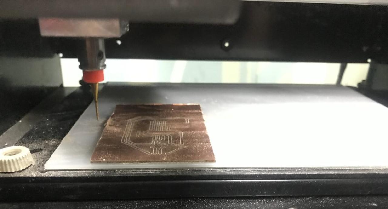
Cutting traces
Cutting the border
The milling we had was not hard enough to cut the copper plate, so it could not be cut, and the routing was complex, so I decided to simplify the edge design.
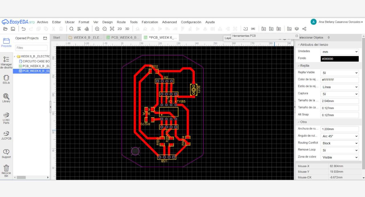
Designing in easyeda
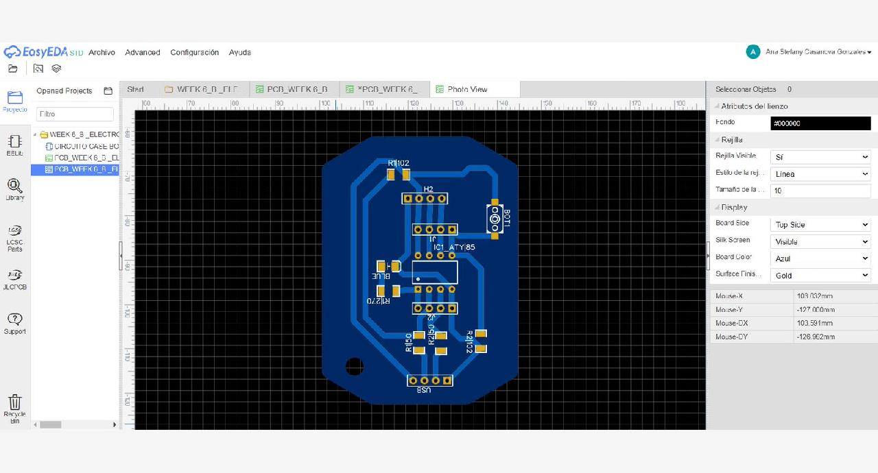
Complete design
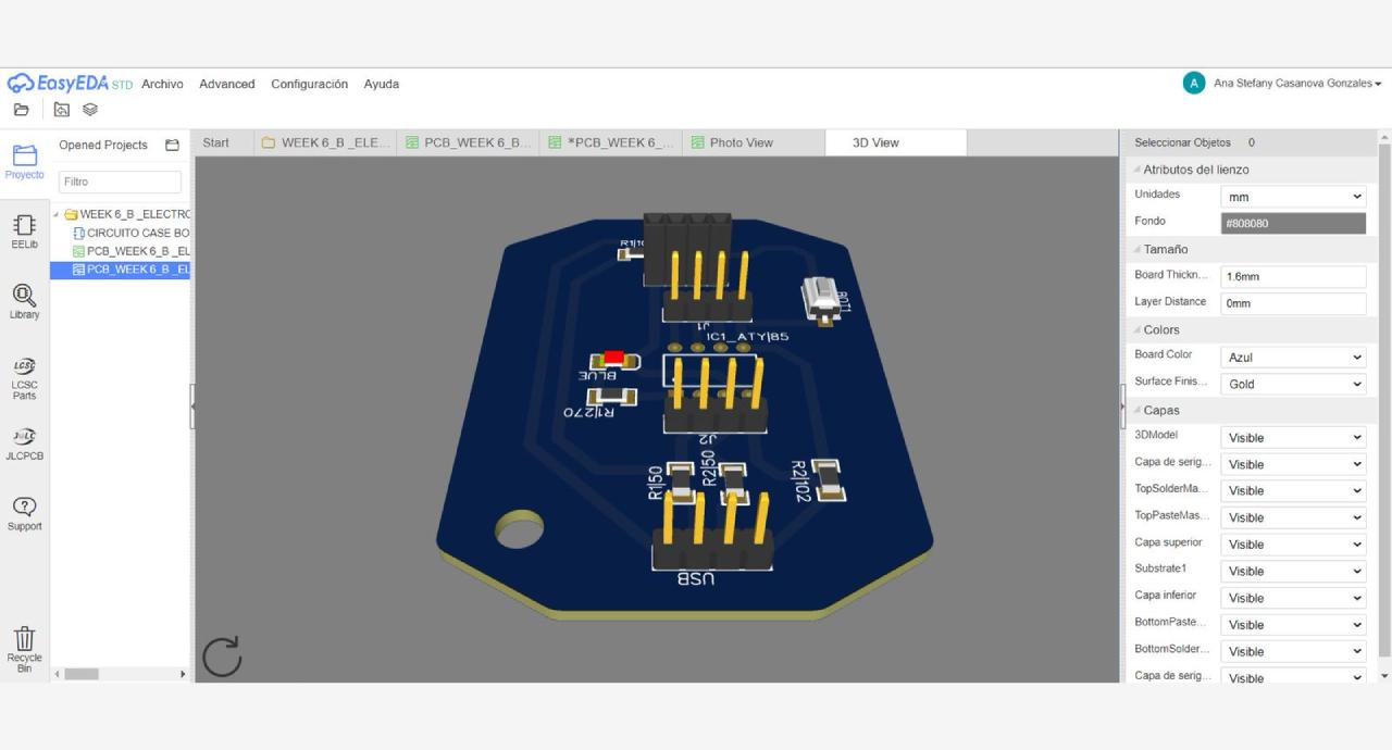
PCB in 3D
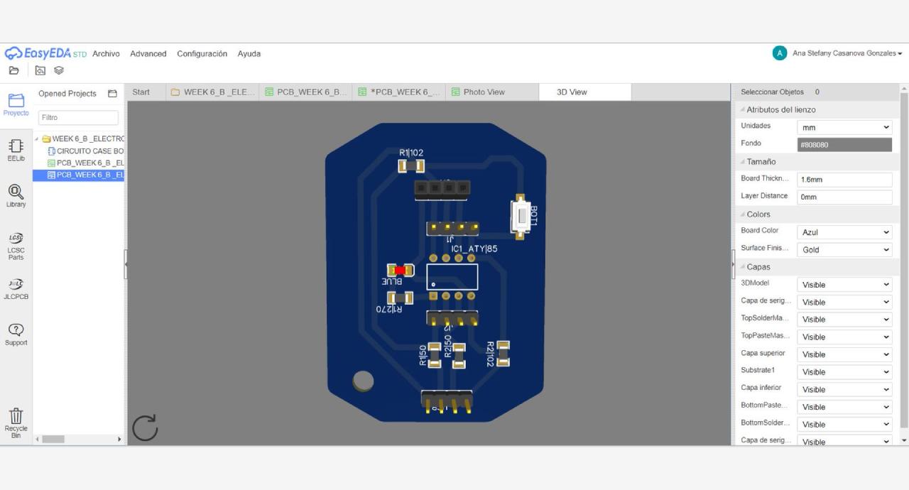
Top view
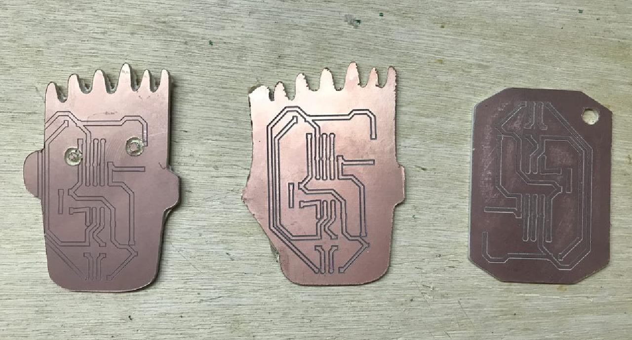
All my PCBs
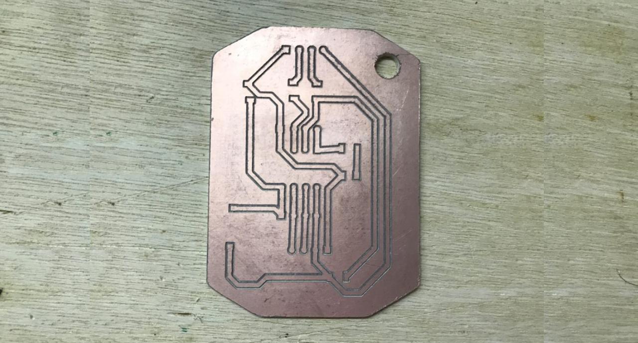
The best detail
As you can see in the process I didn't get some electronic boards with a good detail in the traces, but I practiced a lot the fabrication of electronic boards. Also the copper excess around the traces was not removed. Therefore, I decided to give it one more try. But this time I would design the board for my final project.
The flowchart ofmy final project
Ohmmy 🧡 is my final project, and is a trainer that taught us to breathe with different relaxing rhythms, but like everything in this life, to survive Ohmmy has several jobs. Now he will help us to relax but with more liberating techniques.
Ohmmy will help you get rid of the stress of the day by playing screaming. For this the device will have two microphones, microphone a and microphone b, which capture the scream of each of the players, user a and user b, it receives and senses the decibels of the two screams, it is interpreted that user has the most decibels, the led lights will turn magenta if user A screams louder or cyan if user B screams louder. The winner is the one who screams louder and Ohmmy will tell you who did it.
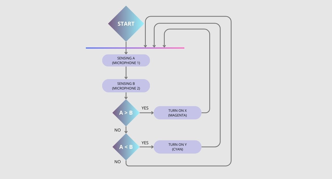
Flowchart
Components
Placing components in Eagle is fun, but ordering them in real life is much more fun. These are the components I used for my final project board. It is true that in Peru they don't sell many of them because they are SMD, however, thanks to Mayra who gave me some that came from Barcelona. I don't know how but I got all of them for this board.
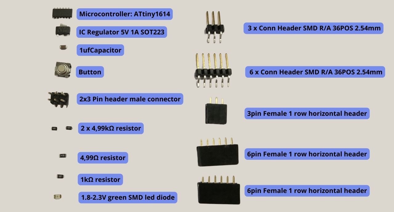
Components
Microcontroller ATtiny 1614
The ATtiny1614 is a compact and efficient microcontroller of the AVR family, designed for simple and low power consumption projects. It has 16 KB of flash memory, 2 KB of SRAM, 256 bytes of EEPROM and operates at speeds up to 20 MHz with a voltage range of 1.8V to 5.5V. It has 12 configurable pins, support for UART, SPI and I²C communication, and is ideal for automation, small device control and specific tasks in electronics. To program the ATtiny1614 in the Arduino IDE, first install support for the microcontroller family from the Board Manager, then connect using a compatible programmer (such as an FTDI module), select the corresponding board and port in the IDE. Finally we write the code, load and run.
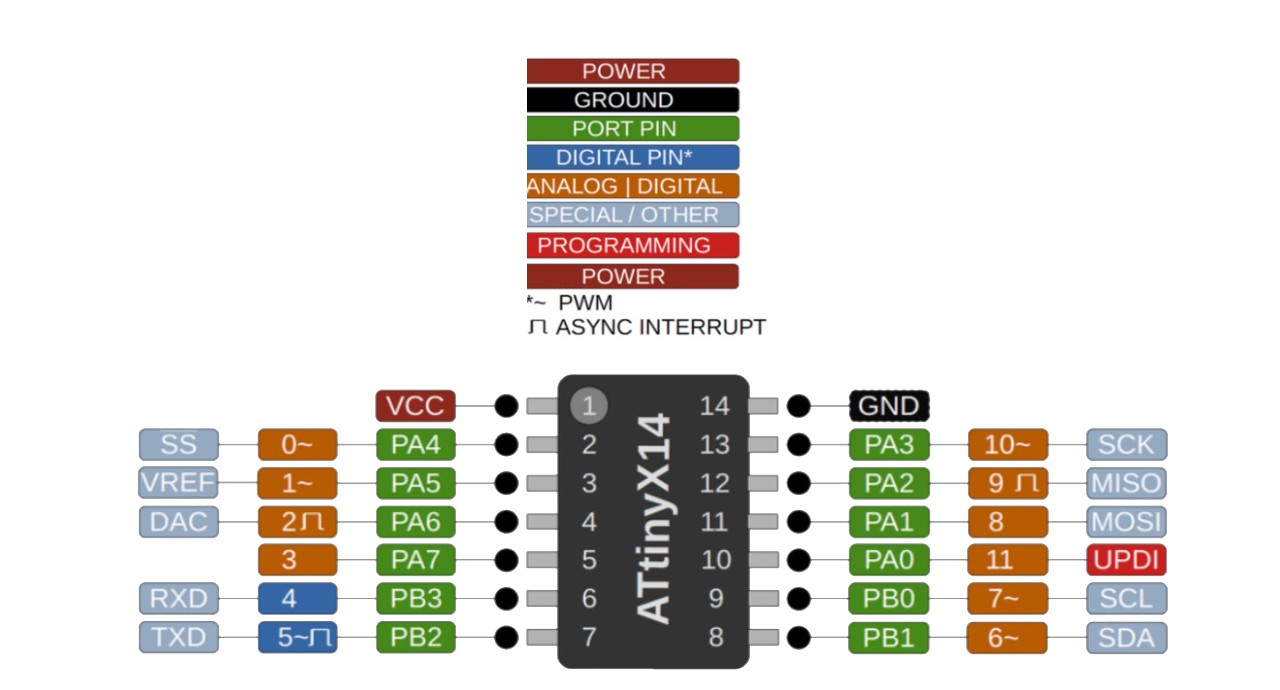
ATtiny 1614 pinout
The last designwith Eagle
After researching, the best option to guide me and make my final pcb board was Adrianino, teh work of Adrian Torres, with this guide I was able to design in Eagle my board, the schematic and the design. It also allows me to export the black and white images that can be processed in any milling software.
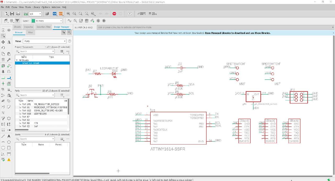
Schematic design
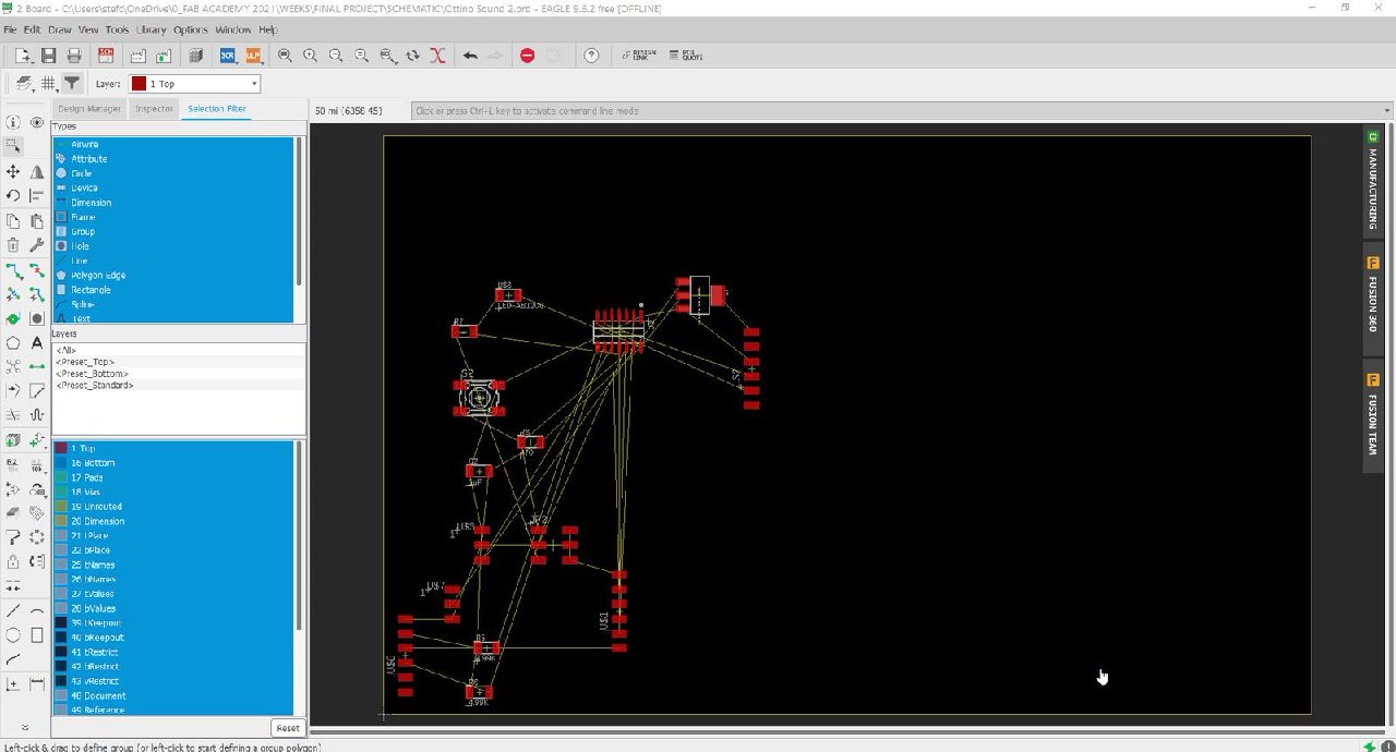
Automatic generation of traces
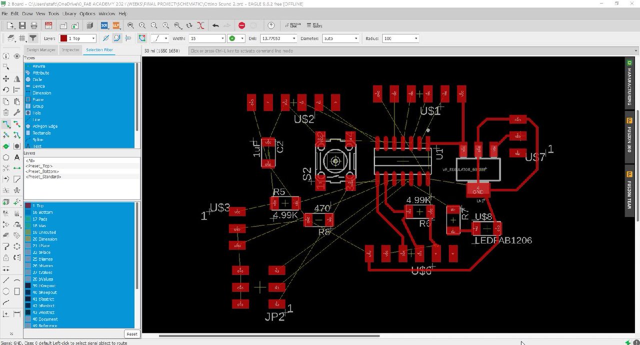
Ordering components
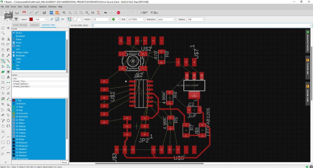
Ordering components
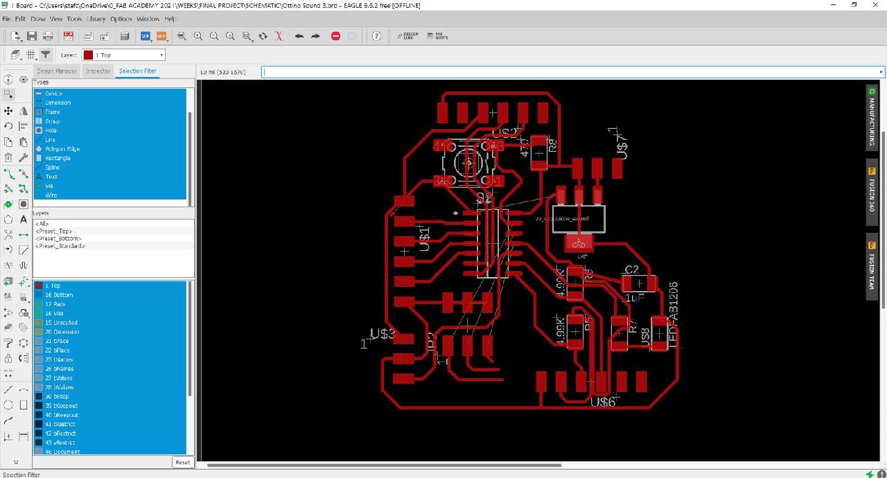
Traces
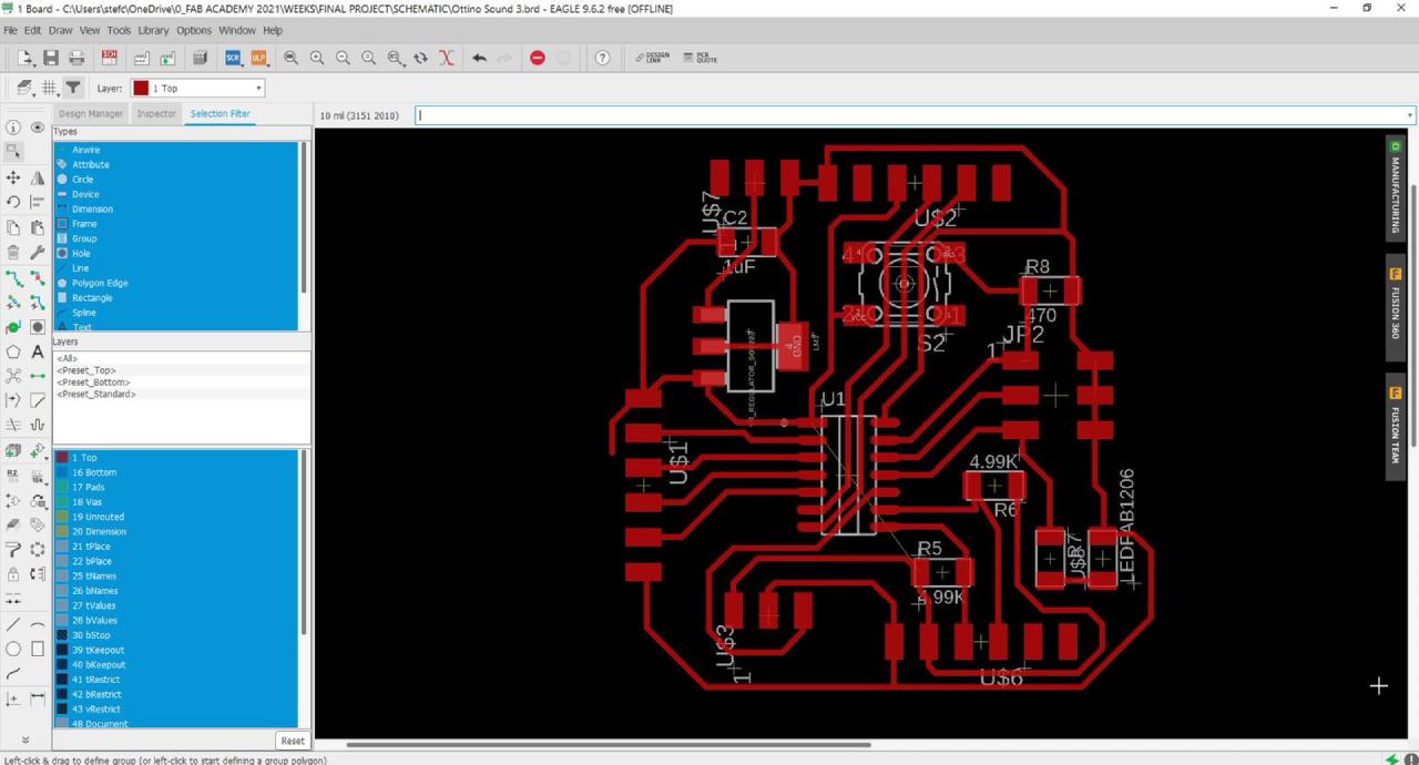
Traces
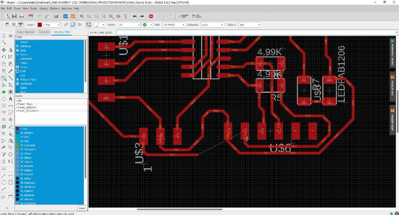
Optimization of traces
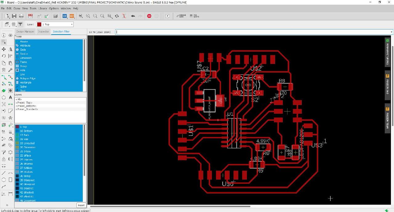
Almost ready
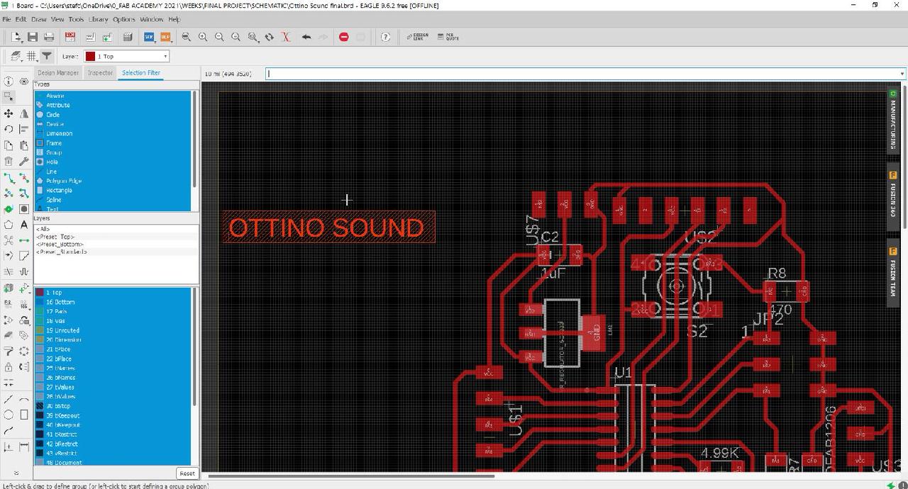
PCB name OTTINO SOUND
After having the traces ready and the components well located it was time to design the edge of the PCB, for this a chain of steps is done as having the vector in Autocad, take it to fusion 360, extrude it and finally import it to Eagle, as all these programs are from Autodesk, they are compatible.
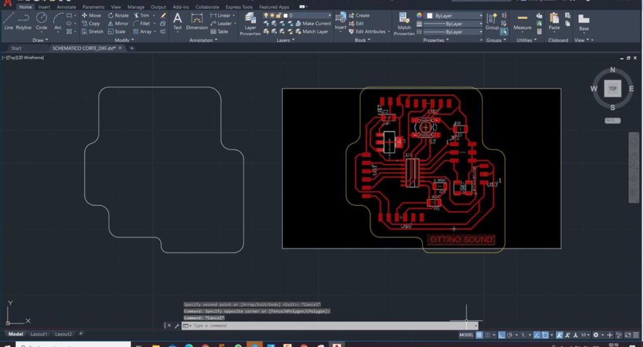
Fusion and CAD
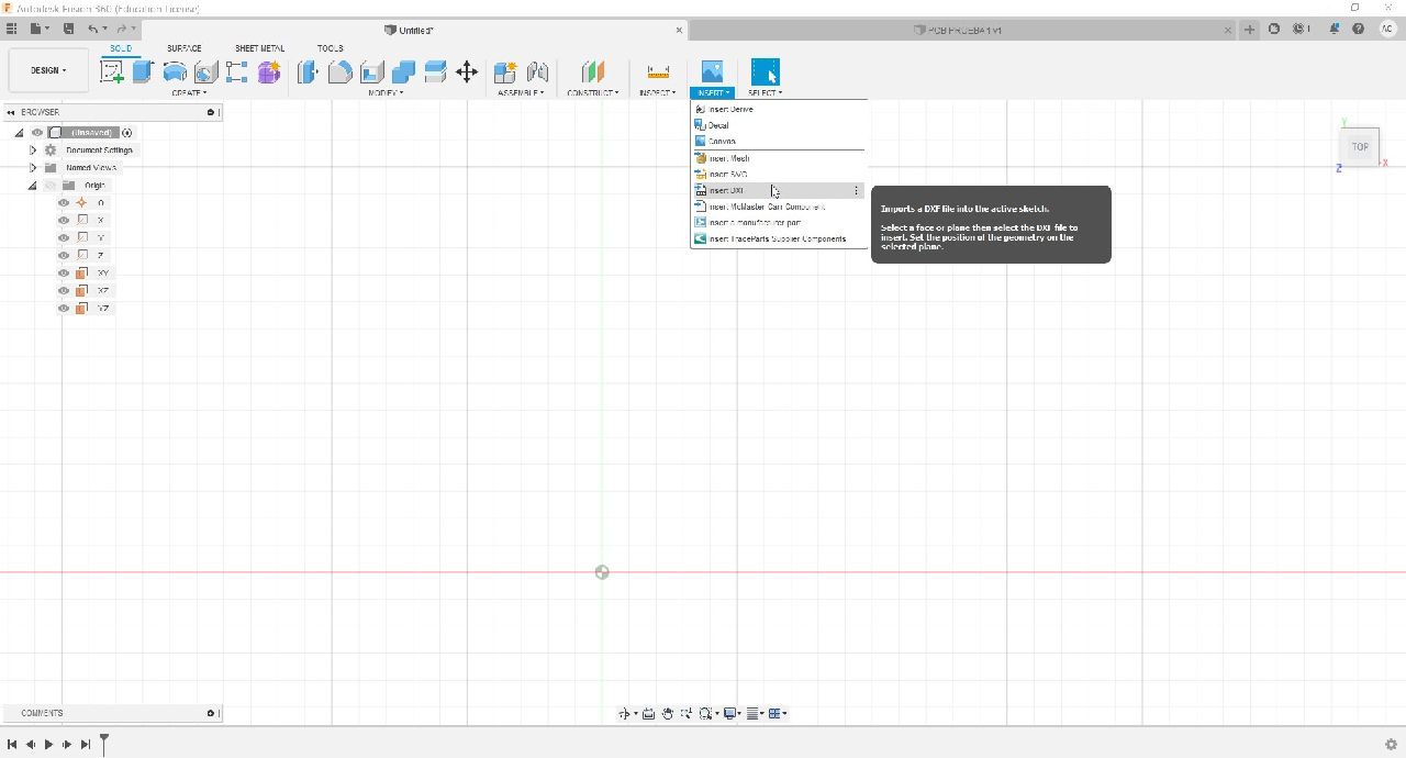
Select Insert DXF
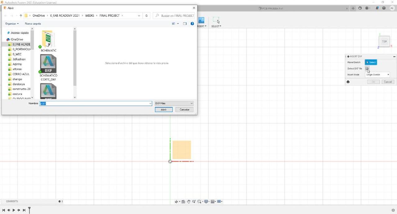
Open the file folder
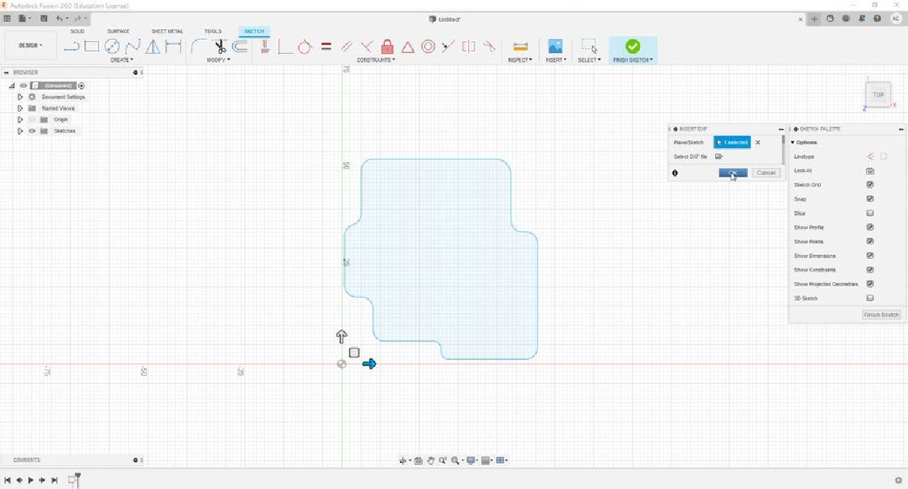
Insert DXF file
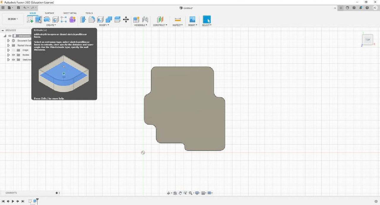
Select Extrude tool
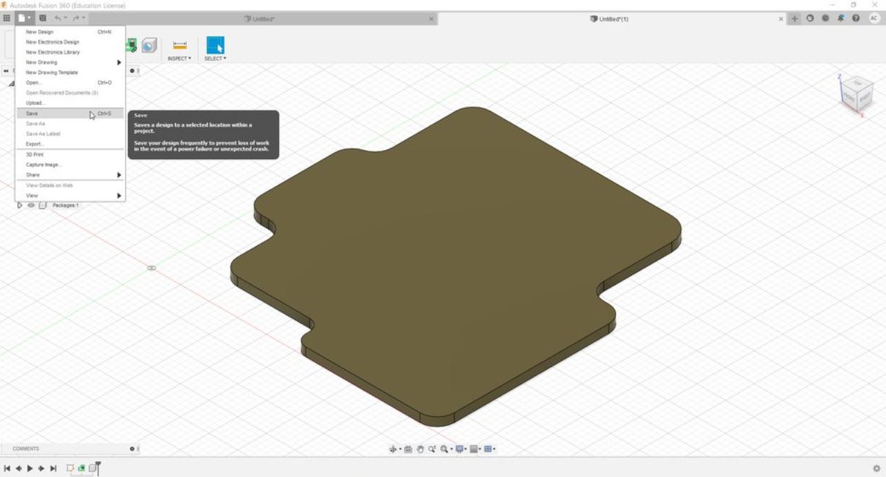
Select the save file option
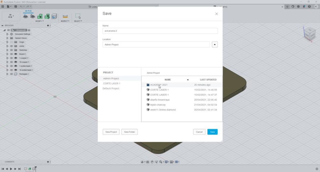
Select route
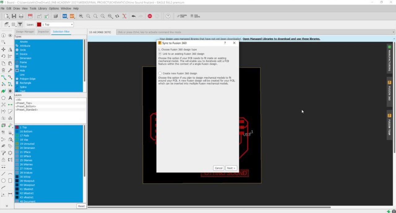
Sync to fusion 360
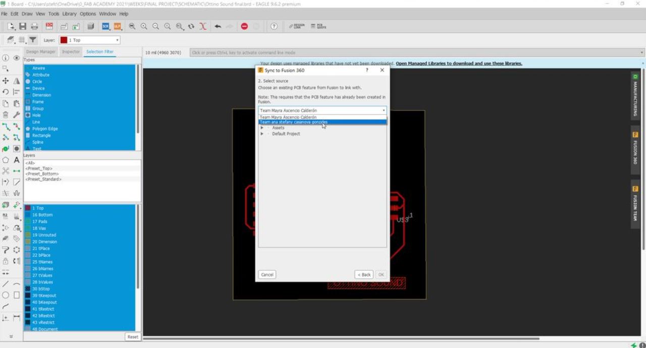
Select source my team
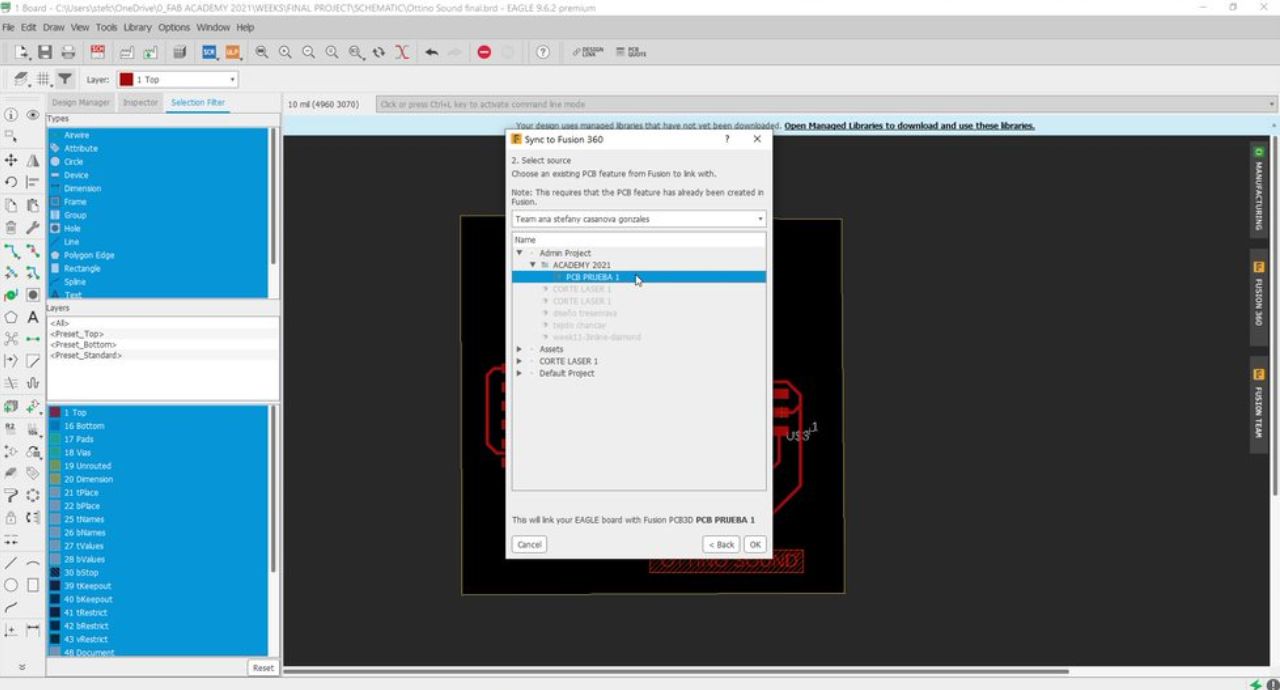
Select PCB test 1
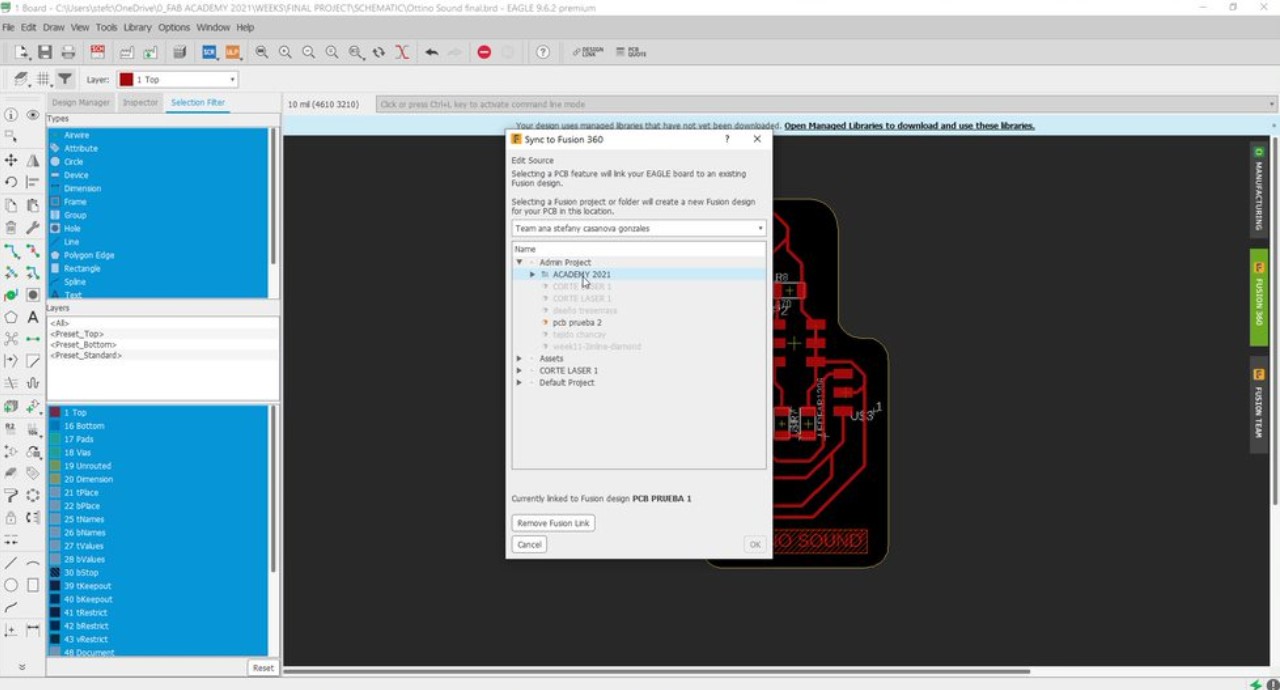
Select PCB test 2
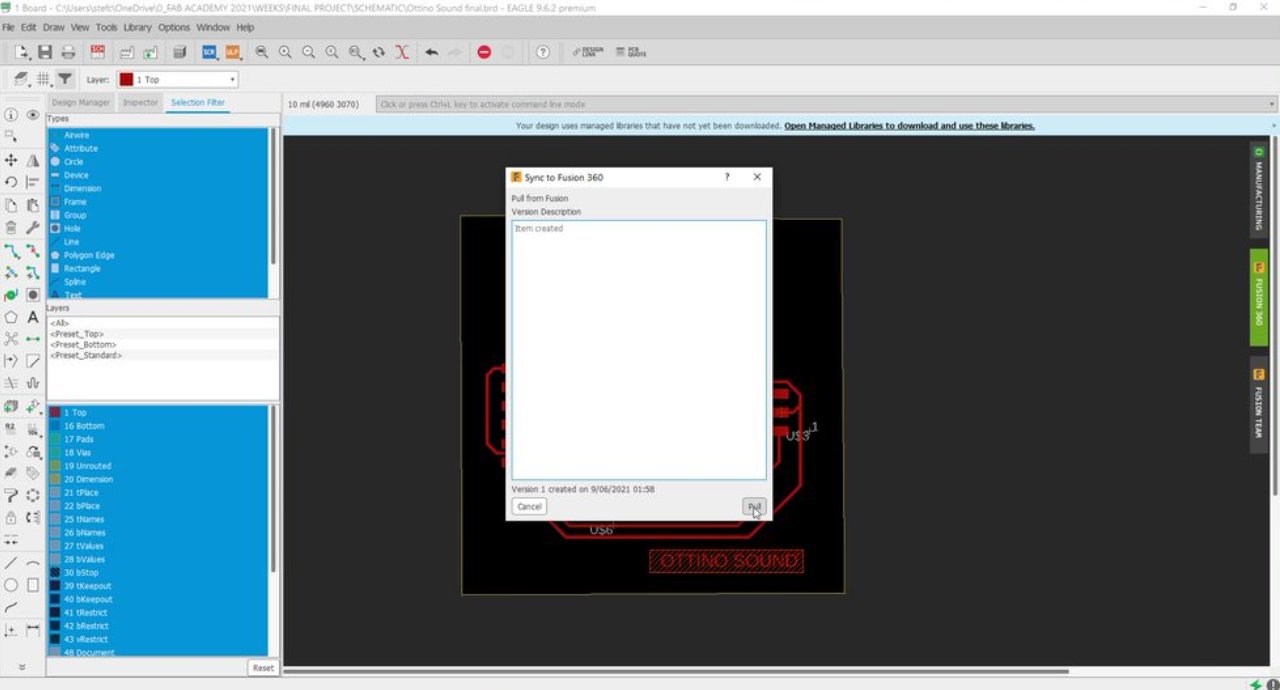
Pull from Fusion
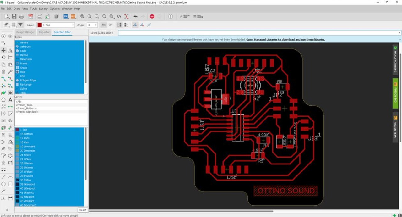
PCB ready!!! 🤗🤗🤗
Ready to cut
Everything was ready for cutting, thanks to Fab Lab Esan and Fab Lab Universidad de Lima who helped Mayra and me to mill these PCBs on the cnc. Then I tested the components on our paper scale diagram to make sure everything was very well designed.
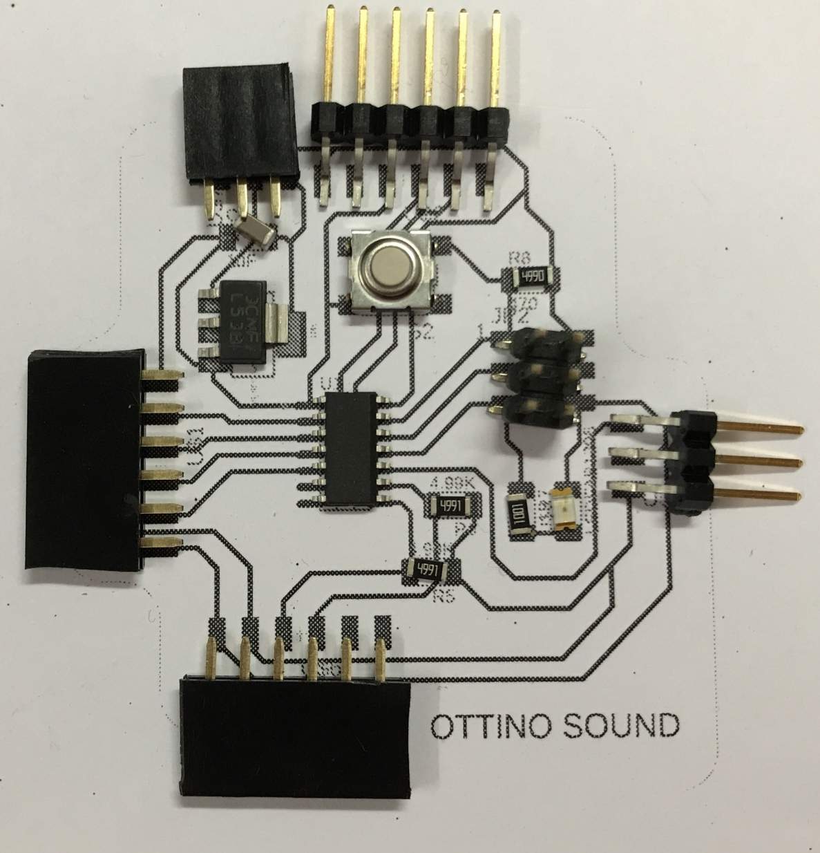
Components presentation
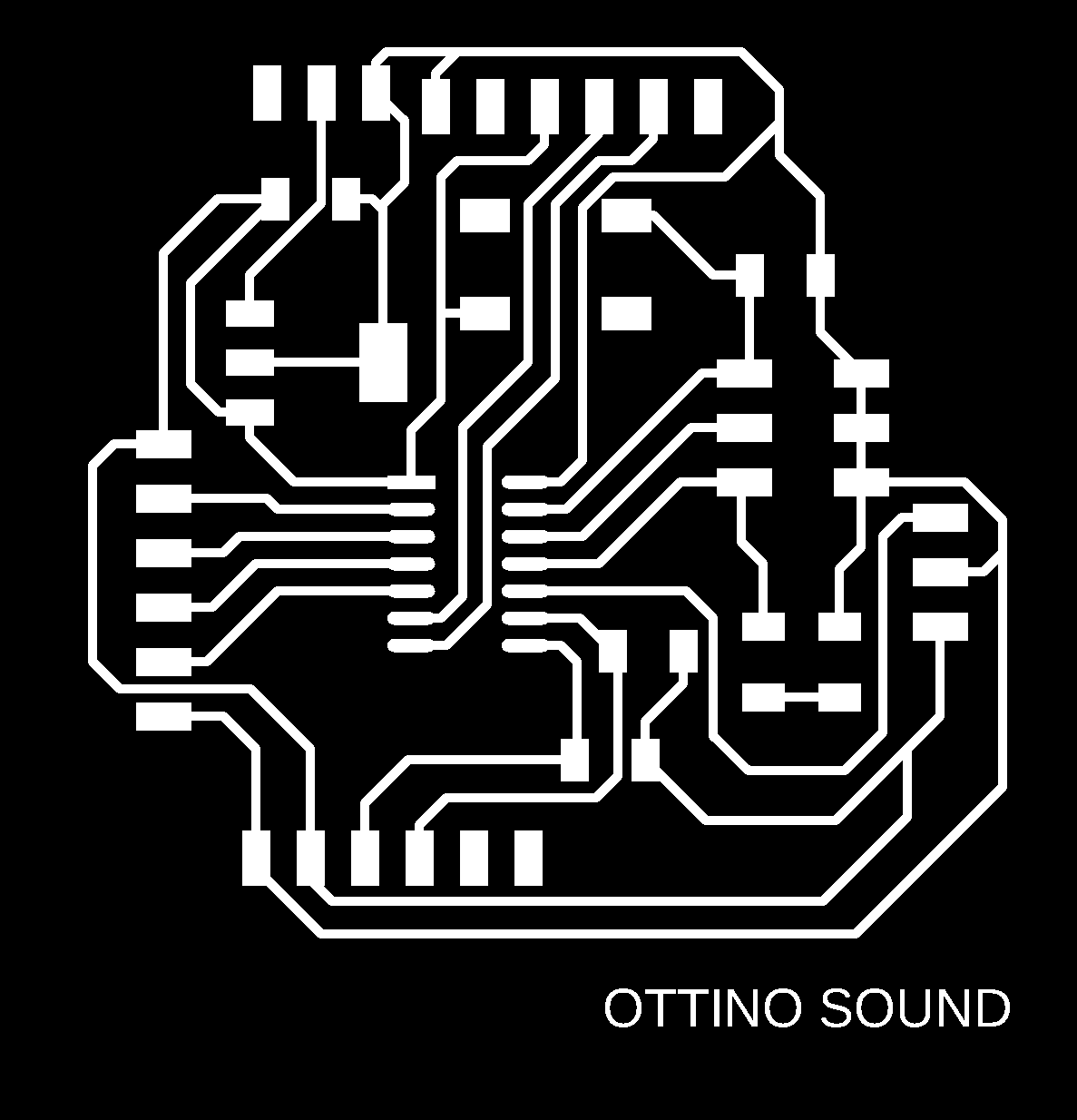
Ottino sound traces

Presentation of components
It was time to mill the PCB board. Everything worked as expected. The traces were very high quality this time. It is reflected in the final result and finish of the board.
Milling my PCB
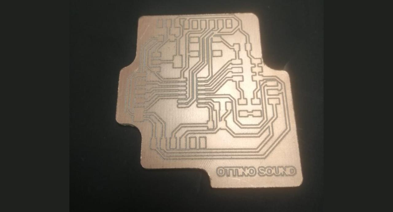
Finished PCB
I fabricated two electronic boards, always thinking that when soldering the components something could go wrong. One has the traces without releasing the remaining copper, and the other one has all the remaining copper removed.
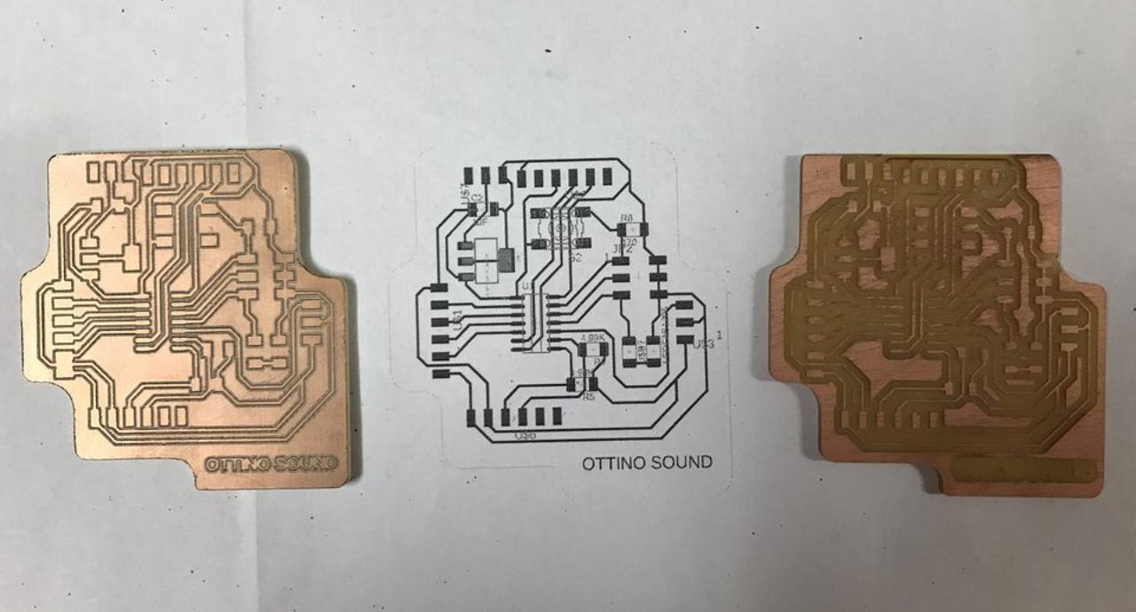
Results
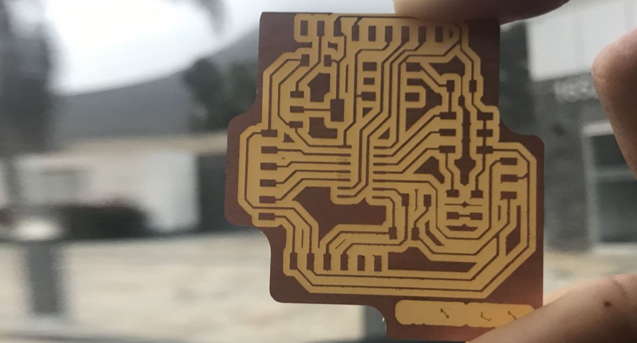
Final result
First practice
Before soldering the components to my board, I did some tests with arduino to understand how to turn on a led from a button. It is a good exercise to work on and understand a little more about electronics, which is not my background.
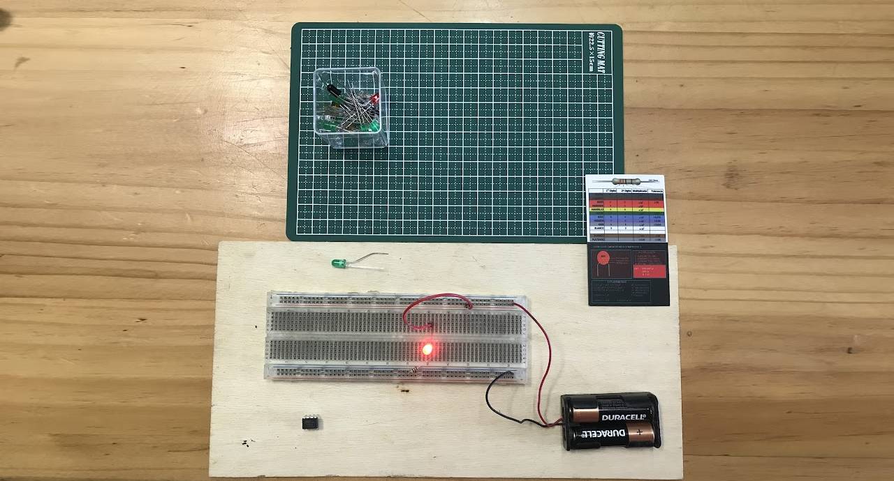
Led and button
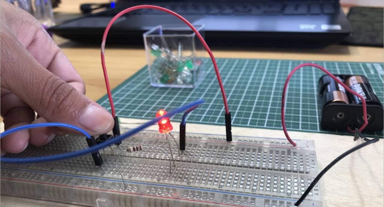
Led and button
Practicing with led and button
Welding my PCB
Together with Mayra, we have had several "soldering stations", at home, at the Detonador workshop in Barranco, Lima, en Moquegua, wherever we can find what we need.
Soldering the components this time was a bigger challenge, they are all very small and they move and fall. Therefore, if you put a soldering point on the board beforehand, then it is easier for the component to "stick".
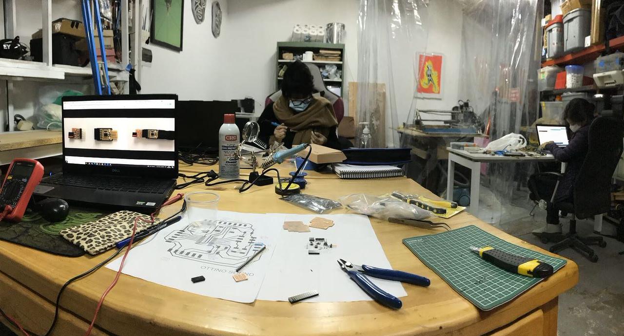
Welding station
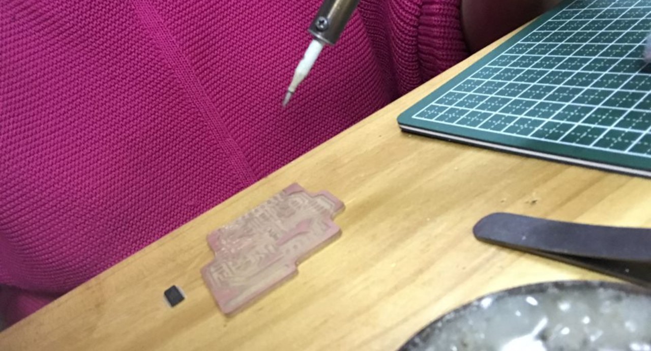
Welding
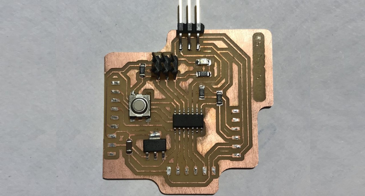
Welded components
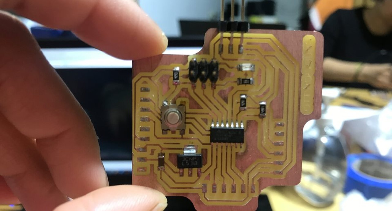
Almost!

Final result!!!🤗🤗🤗
To Connect
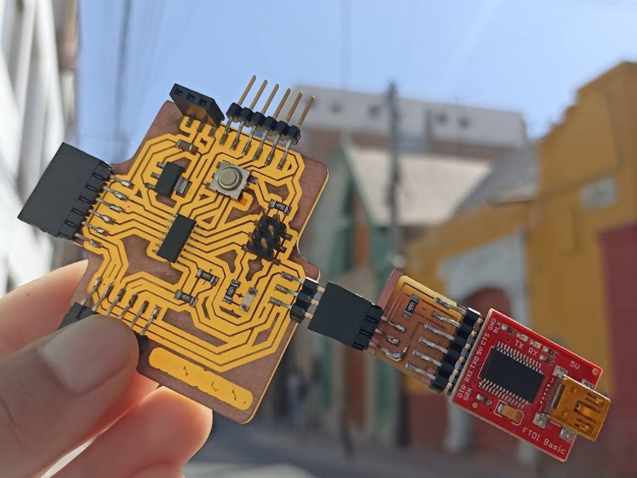
Moving on, I am using a UPDI connector and a SparkFun Basic Breakout FTDI, I had to fabricate the UPDI and purchase an FTDI in order to load programs onto my electronics board.
The UPDI (Unified Programming and Debug Interface) is a carefully designed, central connector that I use to program and debug the ATtiny1614 microcontroller. This microcontroller model uses the UPDI protocol as its primary means for programming and debugging, which is essential for loading firmware and making adjustments during project development.
The UPDI connector operates through three pins: VCC, which provides power, GND, which acts as common ground, and the UPDI pin, which allows direct communication with the microcontroller for program transfer or real-time monitoring of its operation.
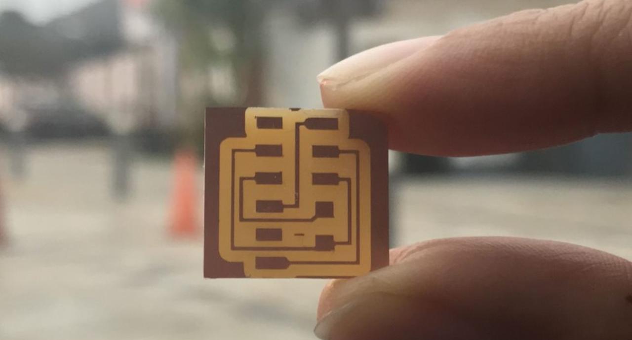
Final result!!!🤗🤗🤗
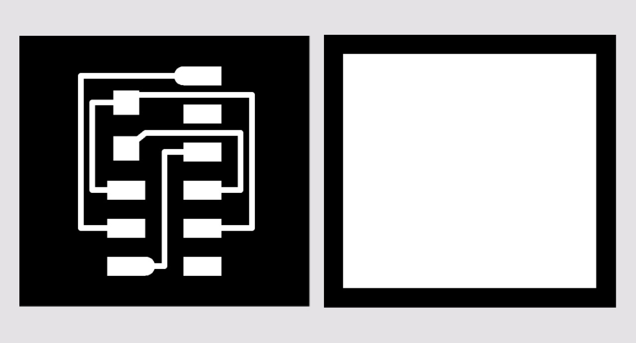
Traces
The FTDI SparkFun Basic Breakout is mainly used to establish serial communication between the computer and the microcontroller, facilitating program loading and debugging during project development. This module is especially useful for sending and receiving data through the UART (Universal Asynchronous Transmission and Reception) interface, allowing to monitor and debug the behavior of the microcontroller in real time or to interact with it through commands.
In addition, the FTDI acts as a converter between USB and TTL signal levels, making it essential for working with microcontrollers that do not have a native USB connection. In this way, it complements the UPDI connector by providing a convenient way to interact with the device while developing or testing. The components are:

Components
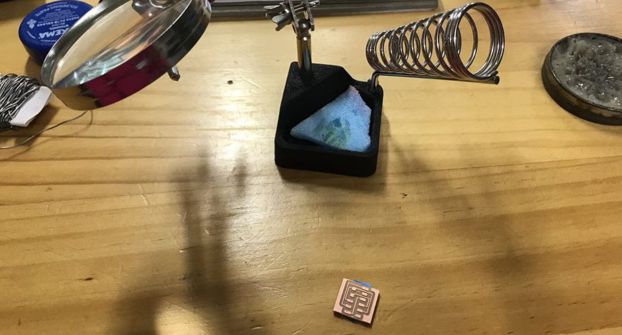
Welding station
Finally I have the whole package ready and soldered, my final board, I called it “Ottino sound”, it is part of Ohmmy 🧡. And it's all ready to go to programming.
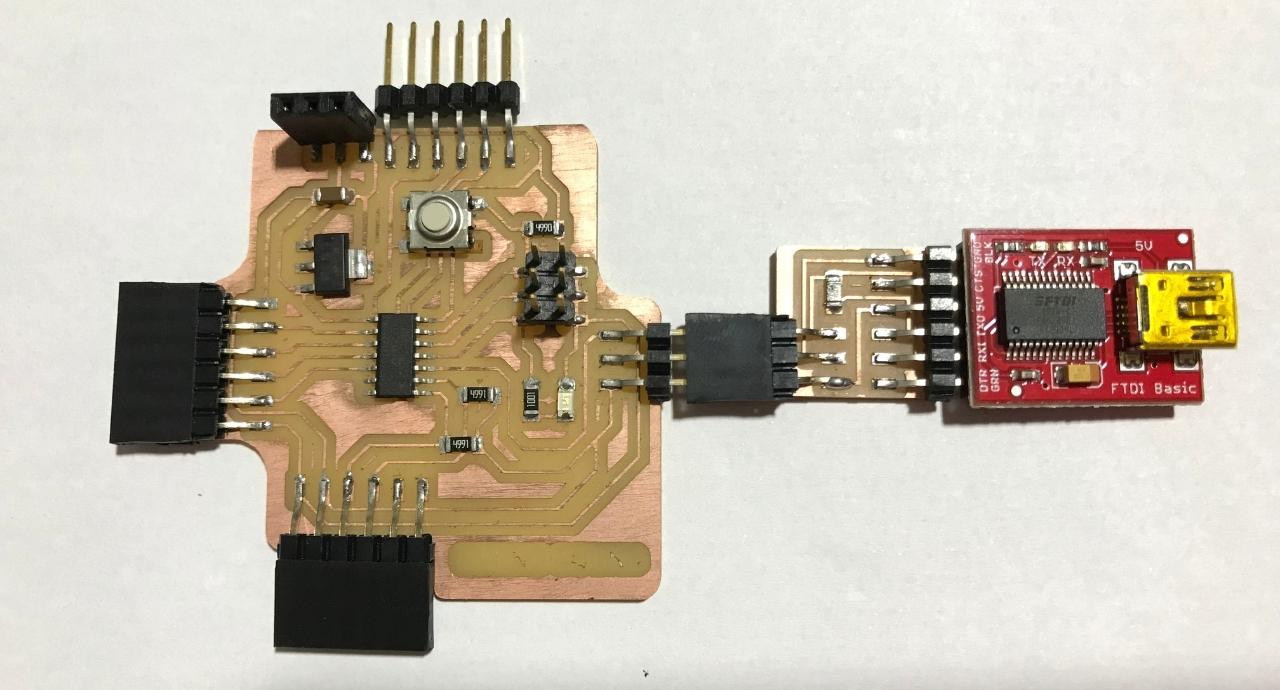
Final result !!!🤗🤗🤗
Programming the PCB
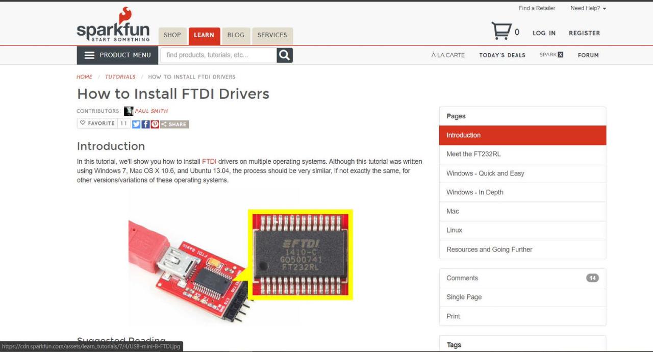
For the computer to recognize the FTDI SparkFun Basic Breakout, it is necessary to install the FTDI drivers available on the official site, use a compatible USB cable that allows data transfer and configure the COM port (in Windows) to identify the device.
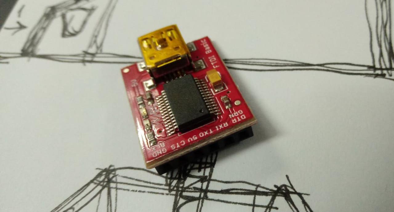
FTDI SparkFun Basic Breakout
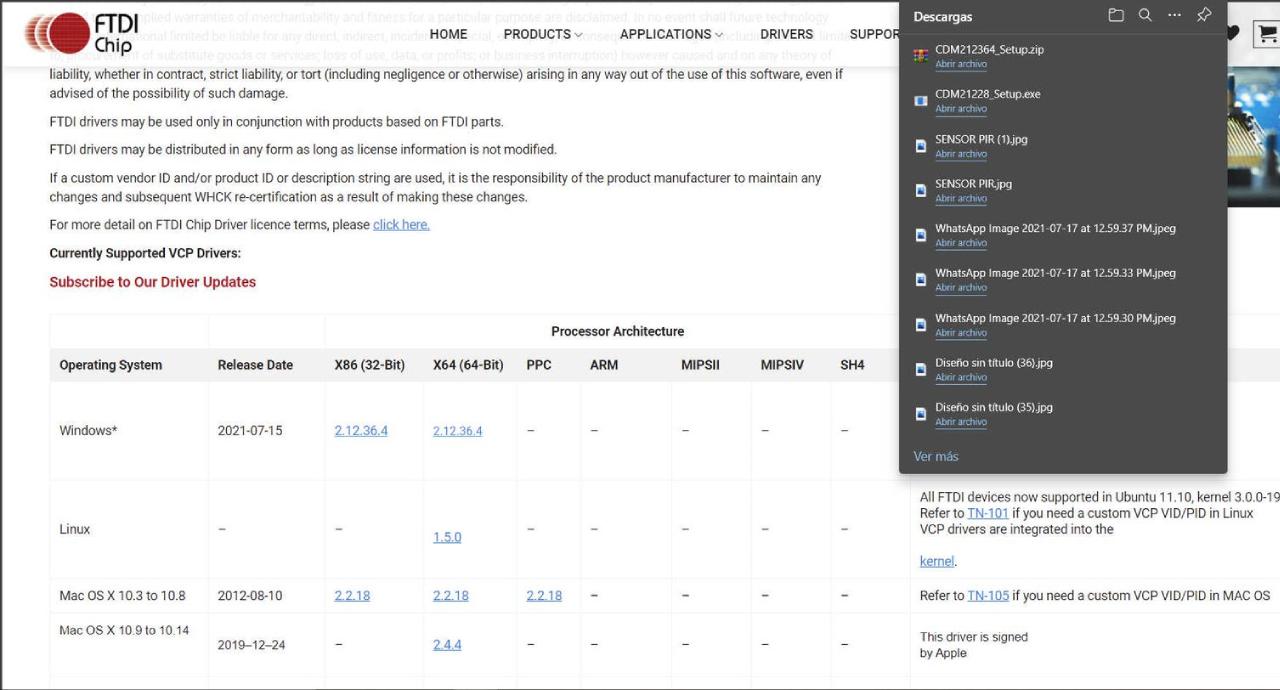
Installing all about FTDI
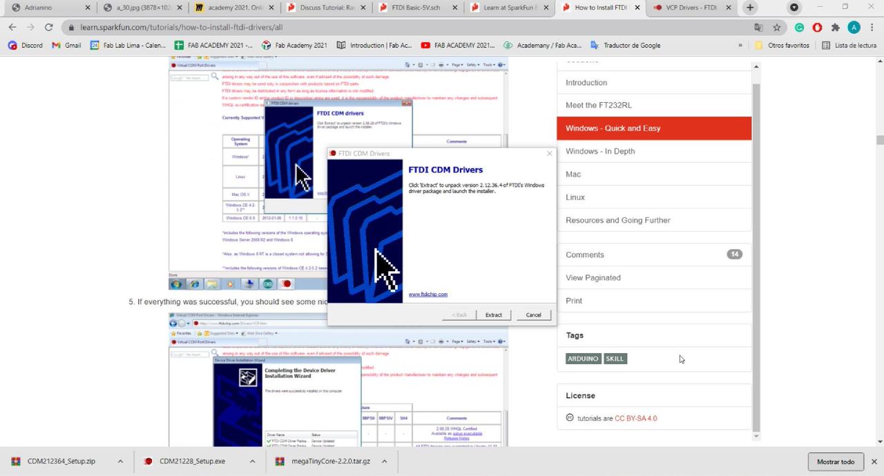
Installing all about FTDI
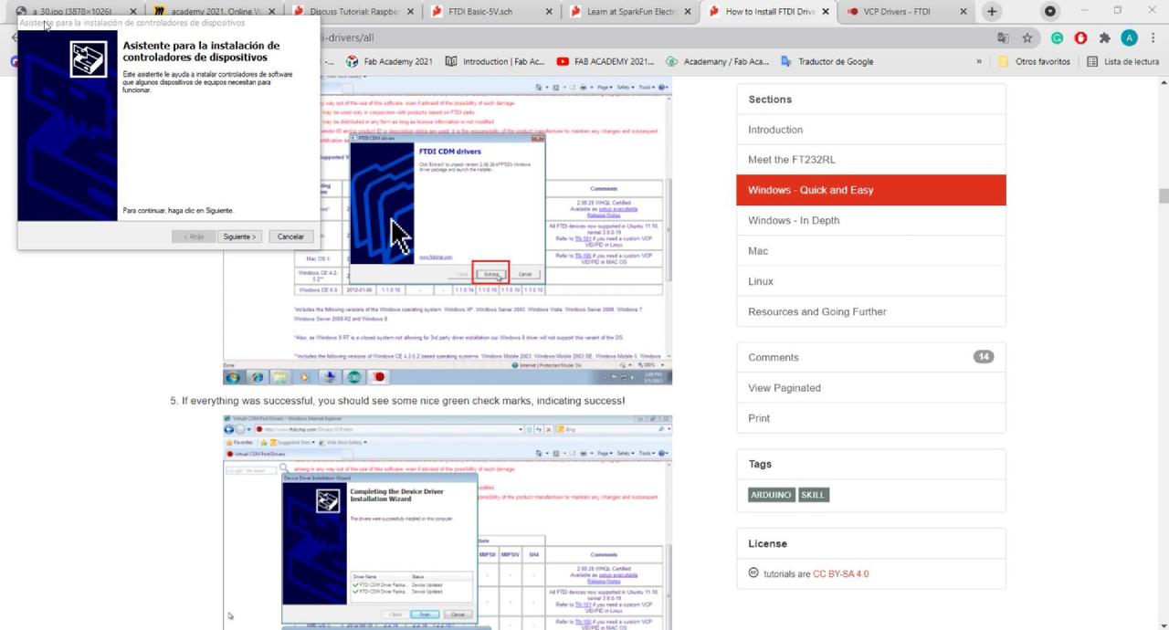
Installing all about FTDI
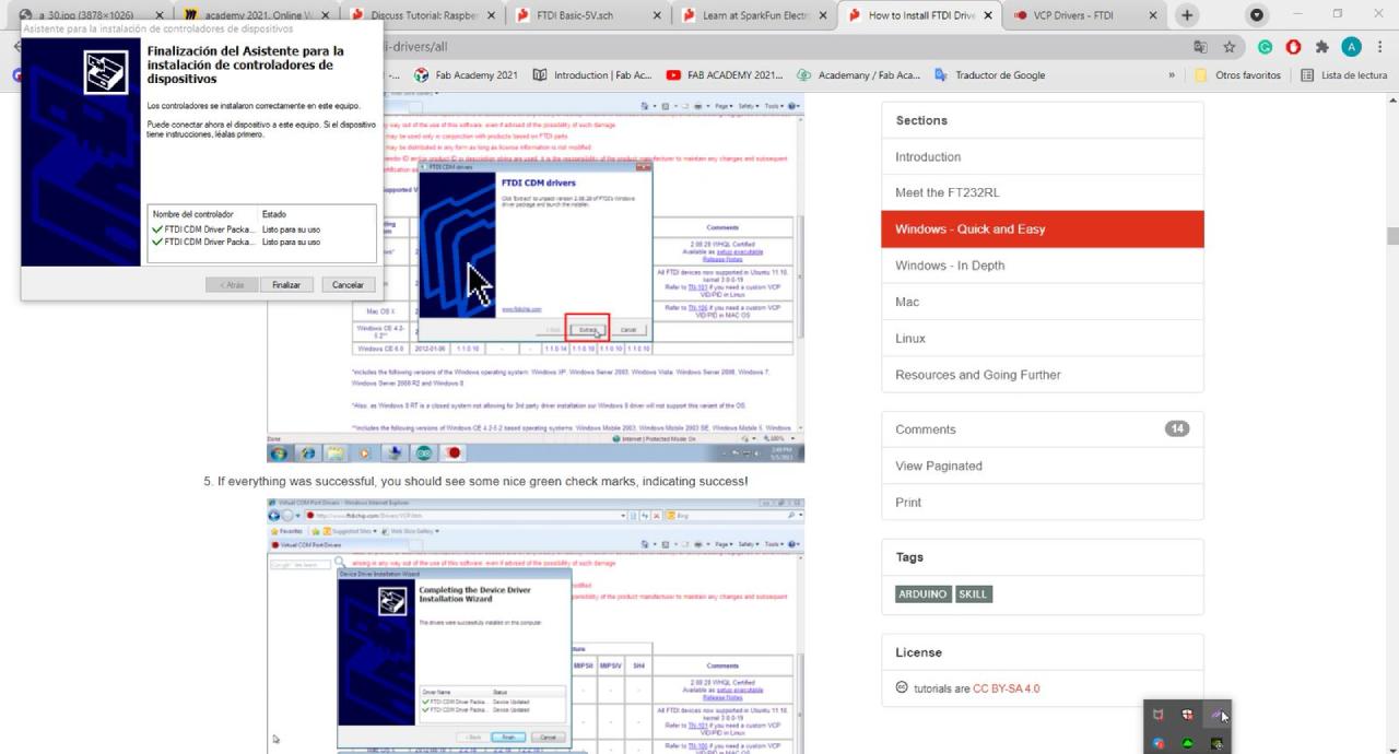
Installing ready
After having everything installed about the FTDI, it is necessary to install everything needed to be able to record my board with Arduino IDE, also choose the programmer, the right board and the COM port. All this in order to burn the “Blink”💡 program to my board.
Using Blink programming on a new electronics board, is crucial because it validates the operation of the hardware by turning an LED on and off, ensuring that the connection and program load are correct. In addition, it introduces users to basic programming and electronics concepts, such as setup() and loop() functions, and the use of digital pins. This simple project allows for easy experimentation with code modifications, encouraging exploration and serving as a basis for developing more complex projects in the future.
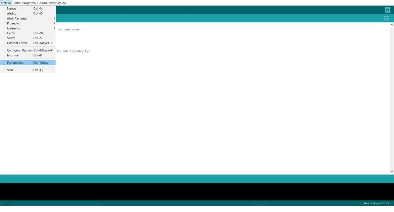
Arduino IDE > File > Preferences
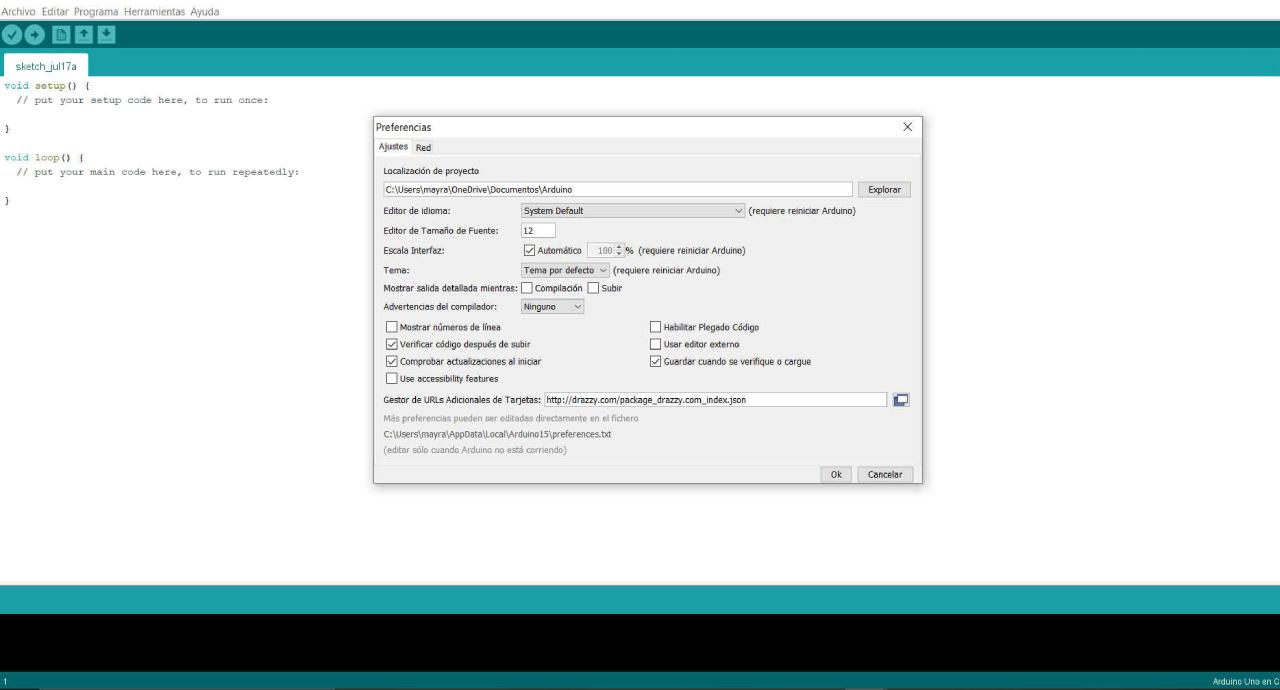
Card url manager
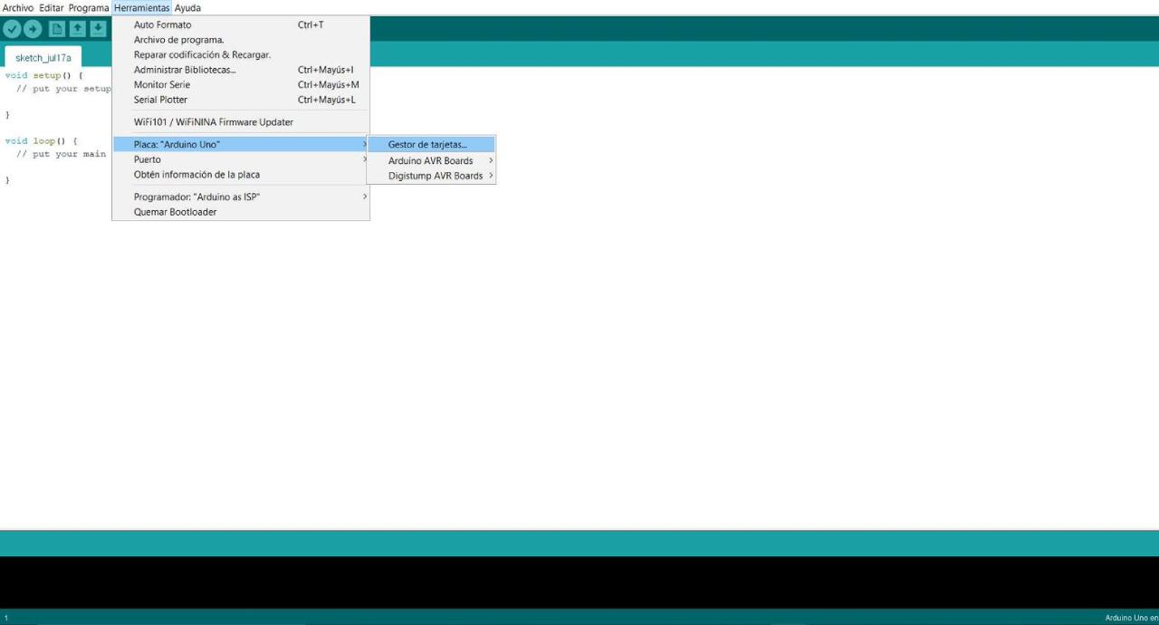
Board Arduino UNO > Board Manager
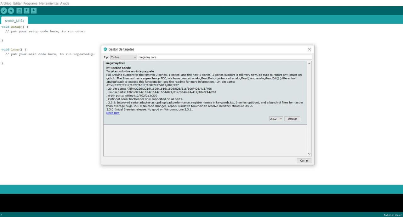
Search Megatiny Core
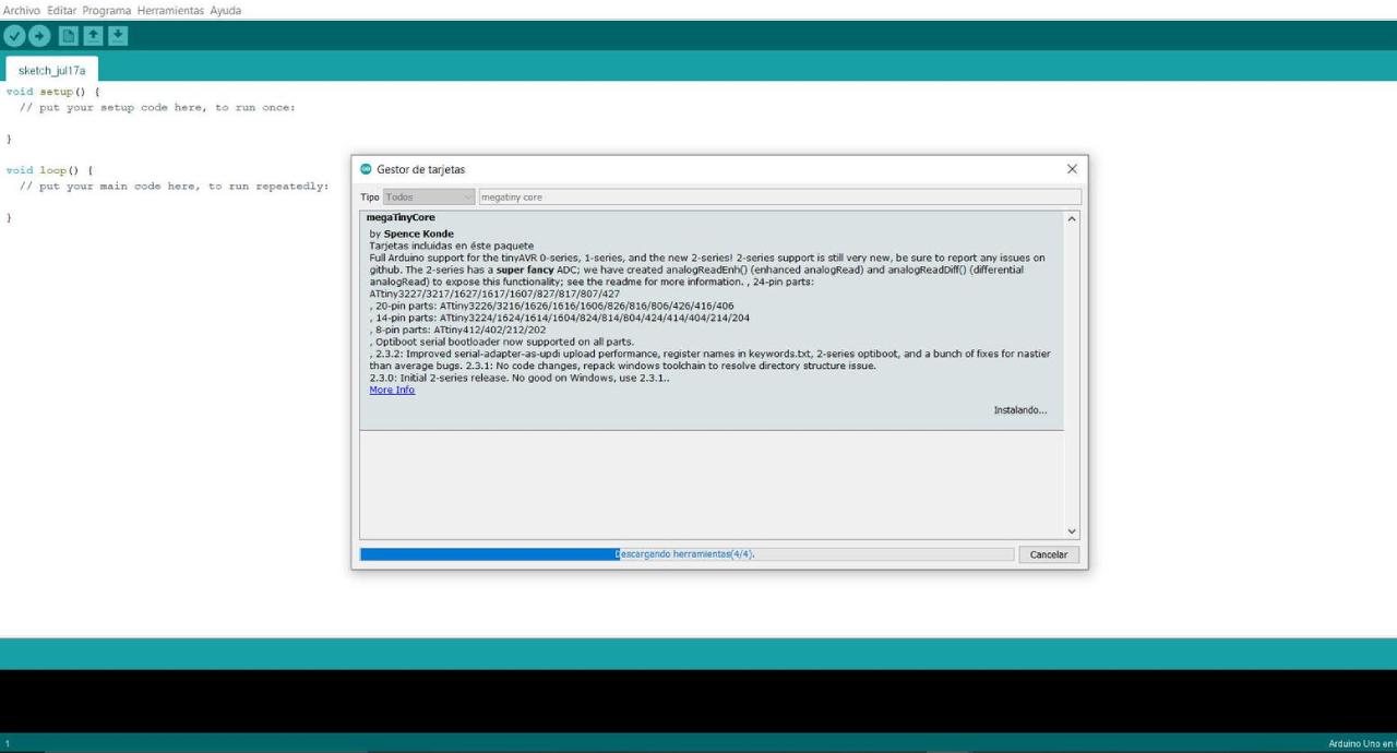
Install MegaTinyCore by Spence Conde
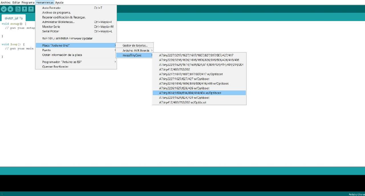
Board Arduino UNO > MegaTinyCore >ATtiny 1614/1604...
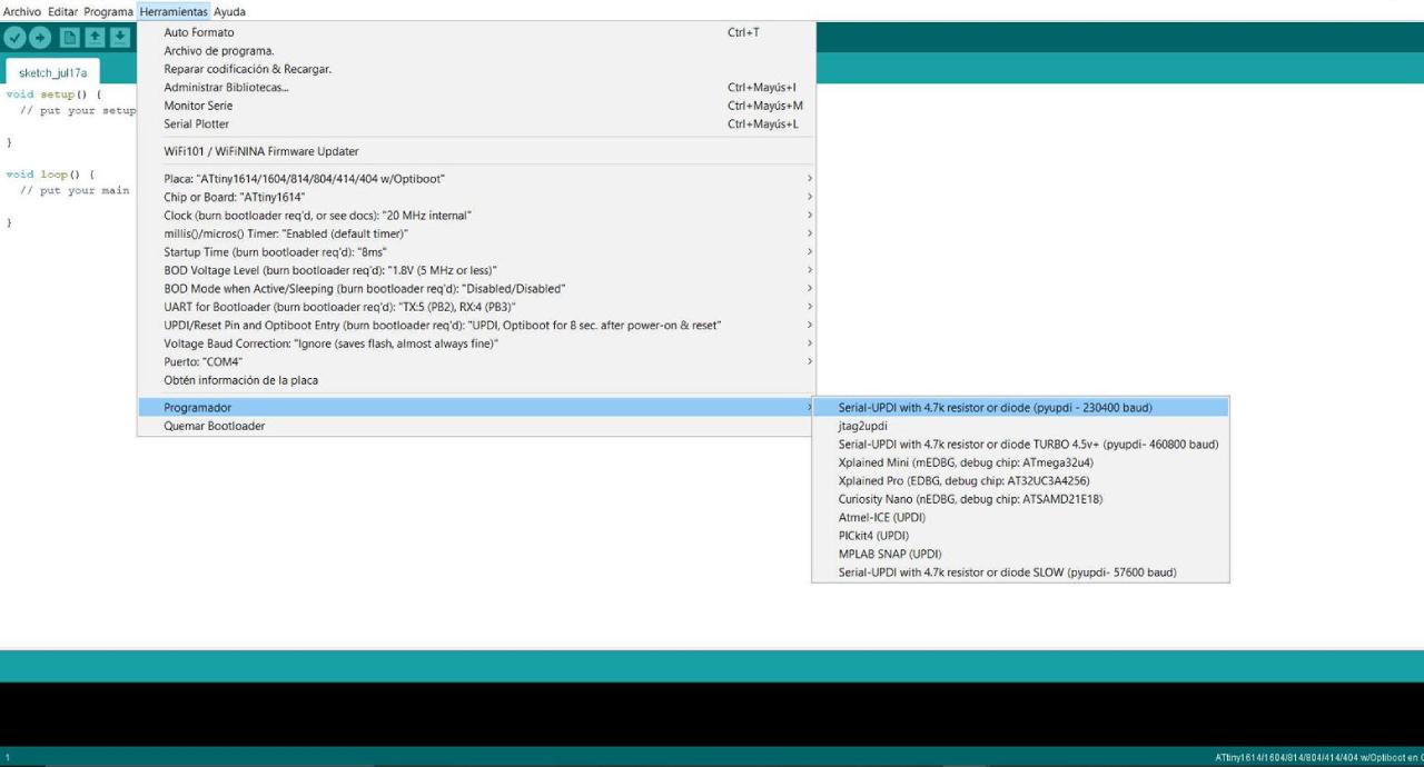
Programmer > Serial UPDI with 4.7k resistor...
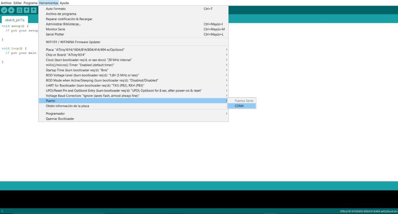
Select Port > COMX
            /*
            Blink

                This example code is in the public domain.

            https://www.arduino.cc/en/Tutorial/BuiltInExamples/Blink
            */

            // the setup function runs once when you press reset or power the board
            void setup() {
            // initialize digital pin LED_BUILTIN as an output.
            pinMode(8, OUTPUT);
            }

            // the loop function runs over and over again forever
            void loop() {
            digitalWrite(8, HIGH);   // turn the LED on (HIGH is the voltage level)
            delay(1000);                       // wait for a second
            digitalWrite(8, LOW);    // turn the LED off by making the voltage LOW
            delay(1000);                       // wait for a second
            }
Arduino IDE Code for Blink
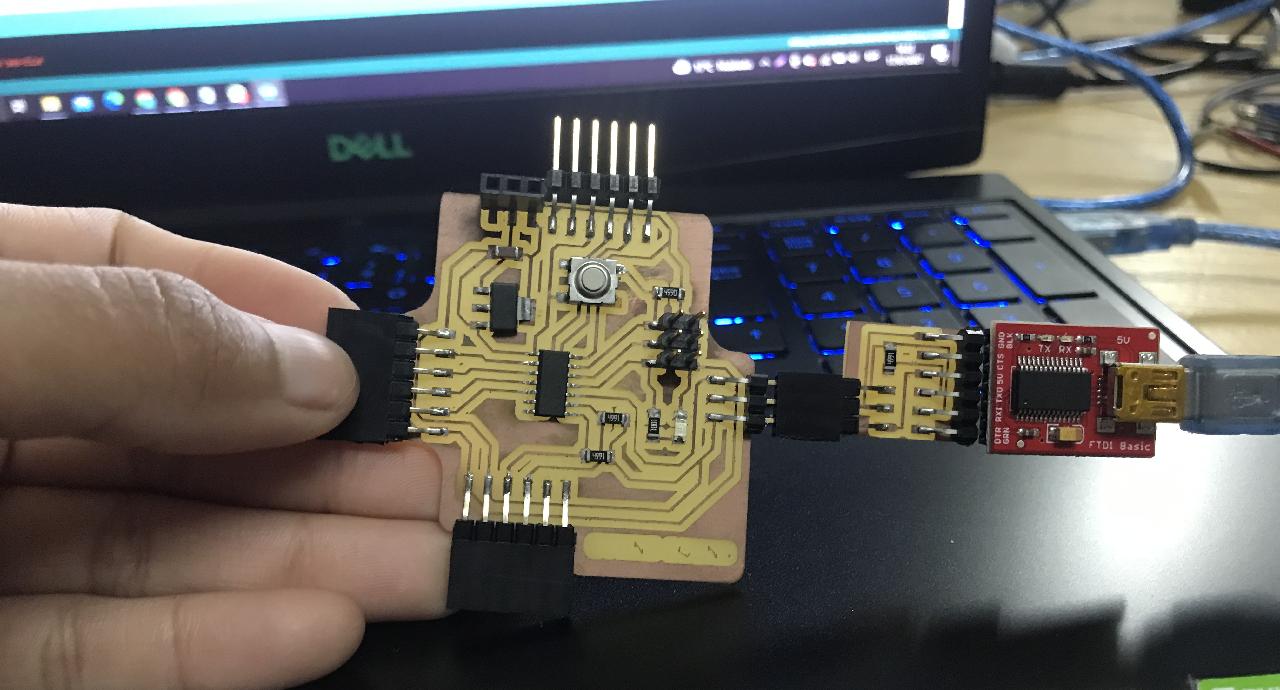
All connected
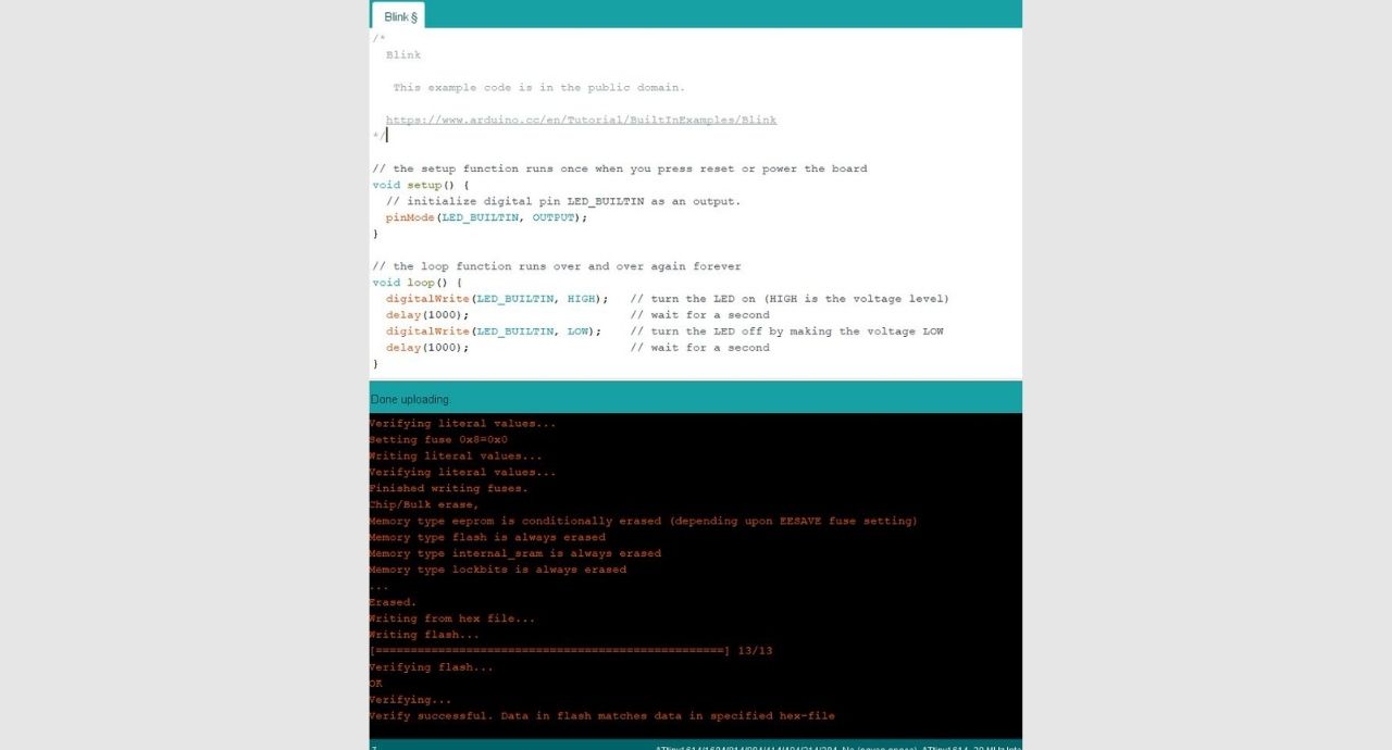
Done!
⭐Blink complete, PCB board working⭐
AboutLearning
- To design electronic boards it is very important to understand the logic of everything!😵 The components, positive, negative, power supply, polarities, the correct position of everything. You have to study and research a lot if you are not an electronics engineer.
- Then comes the second part, connecting the board to the computer and getting it recognized. Then comes the part of drivers, device manager, COM ports, cables among other things I learned.
- Finally, to program the board using the Arduino IDE software, it is necessary to learn the following essential concepts: use of the Arduino IDE development environment, where code is written and uploaded to the board; basic C++ language syntax, including structures such as setup() and loop() to define initial setup and cyclic actions, respectively; and interaction with hardware, such as turning on a led from the button.
My Veredictfrom what I learned
- I learned to have a lot of patience and it is necessary to do a lot of research, but also to ask a lot of questions to understand the electronics a little more.😅
- You must have a lot of pulse, precision and practice to solder such tiny things, it is good to practice before soldering your original board.
- I really enjoyed developing the PCB for my final project and I feel that it is getting closer to becoming a reality.
