5. Electronics production
This week I worked on defining my final project idea and started to getting used to the documentation process.
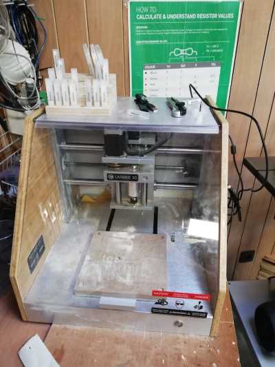
milling the PCB
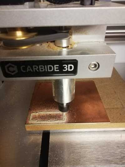
For this part We worked with the nomad. This is a multi purpuse milling machine whit a very userfriendly interface. It is very easy to use even if you have never used a cnc millin machine. the cons of this machine are that it is not Possible to make a lot changes in the paths. But overall a good machine.
I watched the following video before I started.
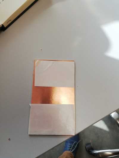
I started whith testing the machine settings. It was a difficult task to do. I tried different settings and differnt tools. At first I noticed that that the machine was not leveled. on some places the cut was good and other places it was to deep. I used 3 kind of tools to the PCB. I used double-sided tape to fix the board to wasteboard.
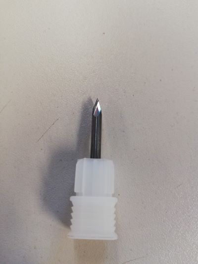
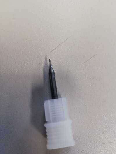
PCB engraver from NOMAD tools
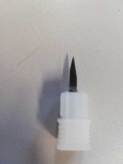
This tool is the standard tool that comes with the machine. It has a angle of 40 degrees. is was difficult to get a small cut with it.
The first tests were not good. You can see that one side is not completely milled. I did found out the tape was to flexible and i pushed one side harder on the board than the other side. After this I used a thinner peace of tape and it was much better.
Square 0.032Ӧ
This tool gave good results for cutting large areas. But the small lines were not good.
PCB engraver
This tool gave the best results for fine lines, for large areas it worked but it took a bit of time.
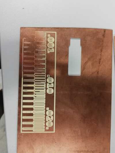
preparing the file
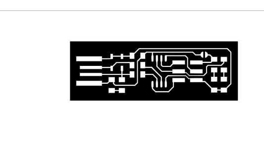
I have prepared the file in inkscape, iT is not the ideal program but it worked.
import the file in carbide create
To prepare the file I used carbide create
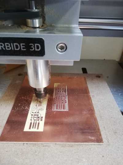
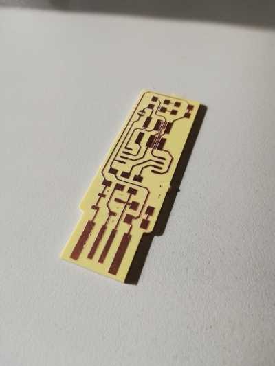
I imported the file in carbide create and made the toolpaths.
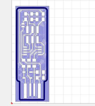
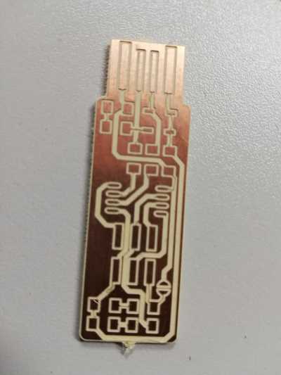
These are the the setting for cutting completely through the board this went very good with no problems.
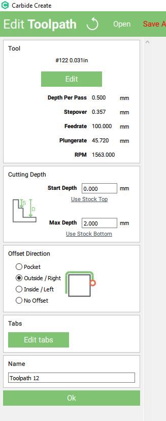
The following settings are for engraving.
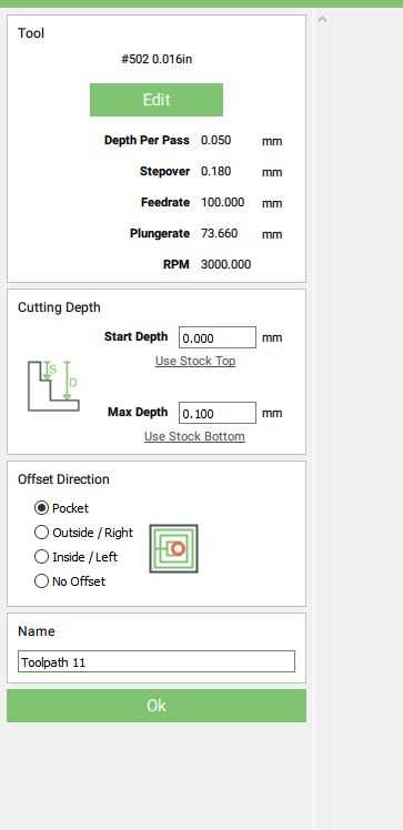
After a lot of trail and error I found the right setting. I changed the depht per pass, the feedrate and the stepover. I did 24 test with different settings.
problems i encounterd
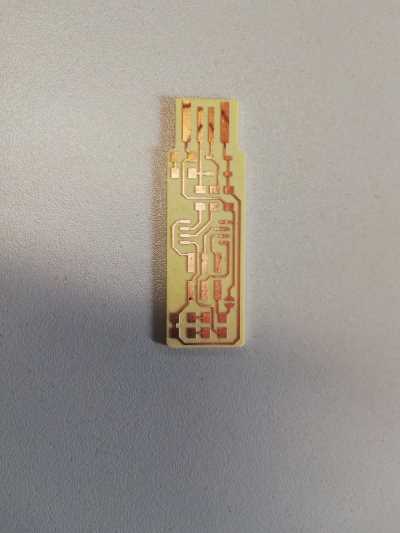
After al the trails and error. i found out that the biggest problem was setting the starting position on the Z-as. I had to do in manually with each job. Each time I put in a new board with new tape it was different. but after all the test I got it right And i had good results.
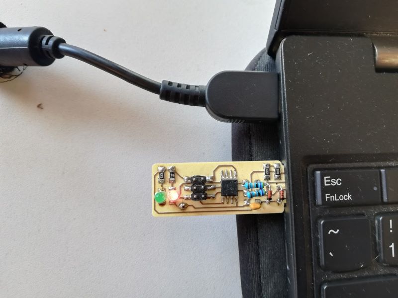
soldering the componets.
I first did some excersise on a failed PCB. I used a lead free solder wire and a soldering station, the tempature i used was 350 degree
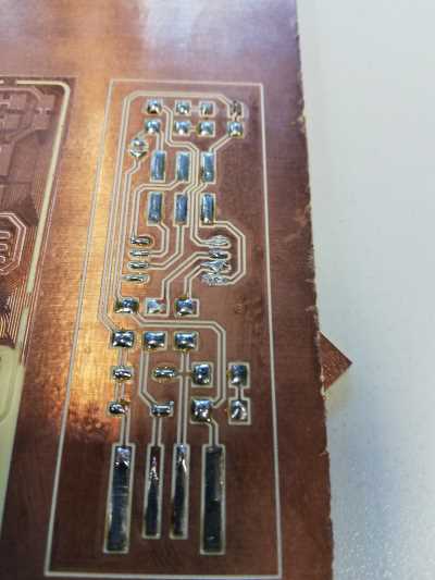
After the excersise i got all the components. The elektro shop did not have all the components in smd so i had to use some bigger parts.
- 1x ATtiny45 or ATtiny85
- 2x 1kΩ resistors
- 2x 499Ω resistors
- 2x 49Ω resistors
- 2x 3.3v zener diodes
- 1x red LED
- 1x green LED
- 1x 100nF capacitor
- 1x 2x3 pin header
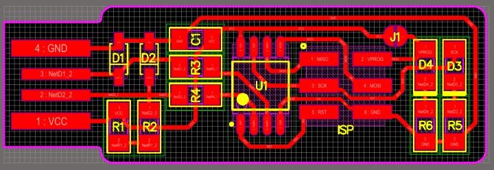
- R1= 1k
- R2= 499
- R3= 49
- R4= 49
- R5= 499
- R6= 1k
- D1 & D2 are the 3.3v diode
- D3 is the green led, and D4 is the red led
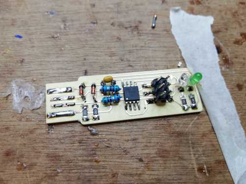
I did lose a lot of time to find the components and I didnt understand the assiment completely. I did understand how to mill the board but not what is was for. I remilled the board with the correct dimensions.
programming the board
This was the hardest part of the course until now, i did not completely understand the logic that I had to follow. It was the first time I did something like this. I had help from benny in the lab and he helped me through this. He showed me to use an arduino as ISP to program the programmer.
We used the following video as help for this.
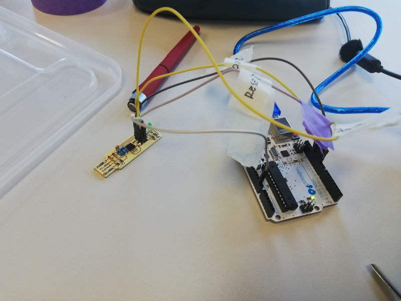
setup ardiuno
I connected the board to the arduino
13 –> SCK 12 –> MISO 11 –> MOSI 10 –> RTS GND –> GND 5V –> V