4. Electronics production
This week’s homework:
1. group assignment: characterize the design rules for your PCB production process.
2. individual assignment: make an in-circuit programmer by milling and stuffing the PCB, test it, then optionally try other PCB processes.
Fablab Digiscope has a fiber laser cutter, so we’ll be using this machine for our PCBs.
Fab ISP Laser Engraving
I’m going to be building the Brian Fab ISP:
http://fab.cba.mit.edu/classes/863.16/doc/projects/ftsmin/index.html
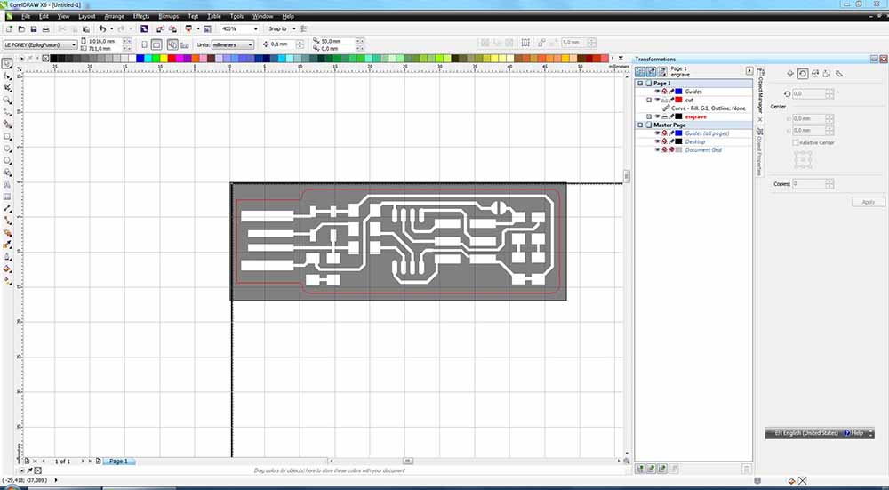
I first downloaded the two circuit images and saved them to a USB stick. I loaded them into Corel draw.
In Corel Draw I created two layers, one for the PNG to rater engrave, and the second as the board outline to cut in vector format.
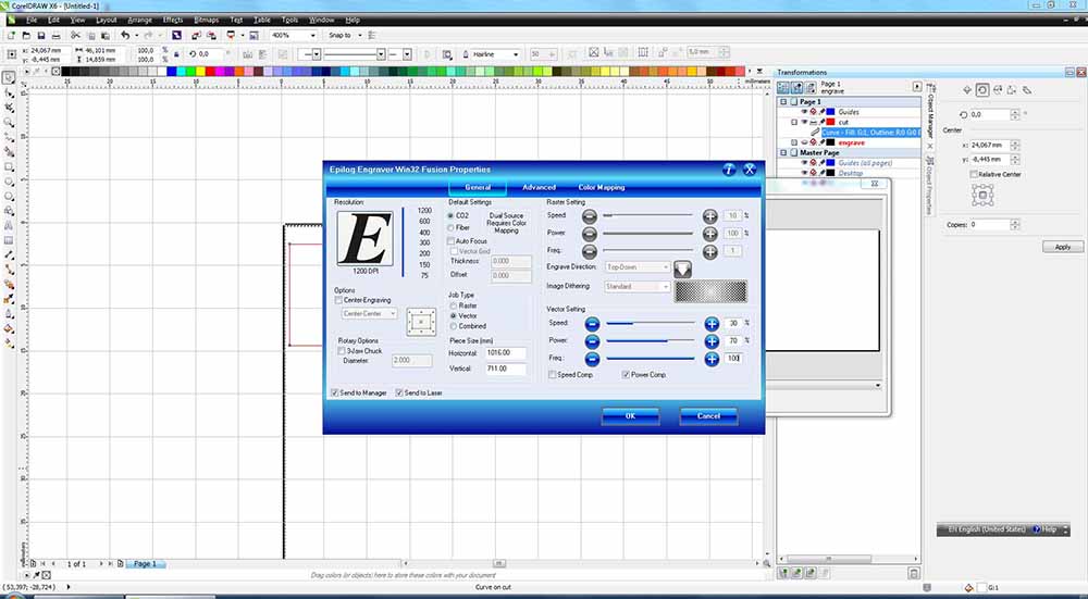
Here are the Fiber laser settings for the raster image: 1200 DPI, 10% speed, 100% power, 1 frequency. These settings are based on previous tests done at the fablab.
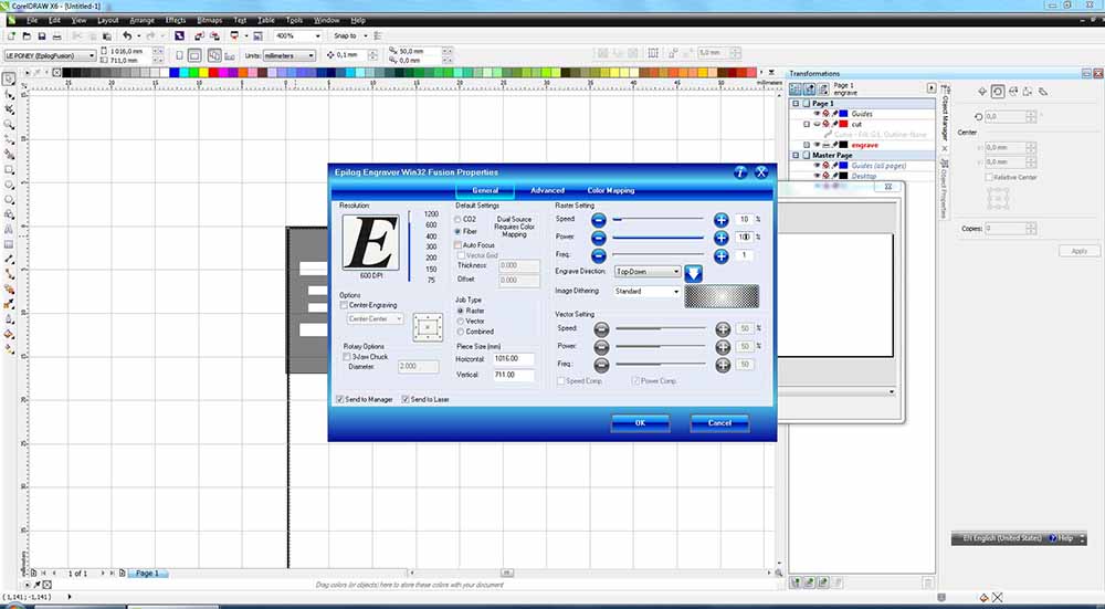
Here are the settings for the CO2 laser to cut out the board outline in vector mode: 30% speed, 70% power, 100 frequency.
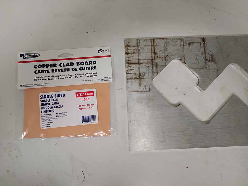
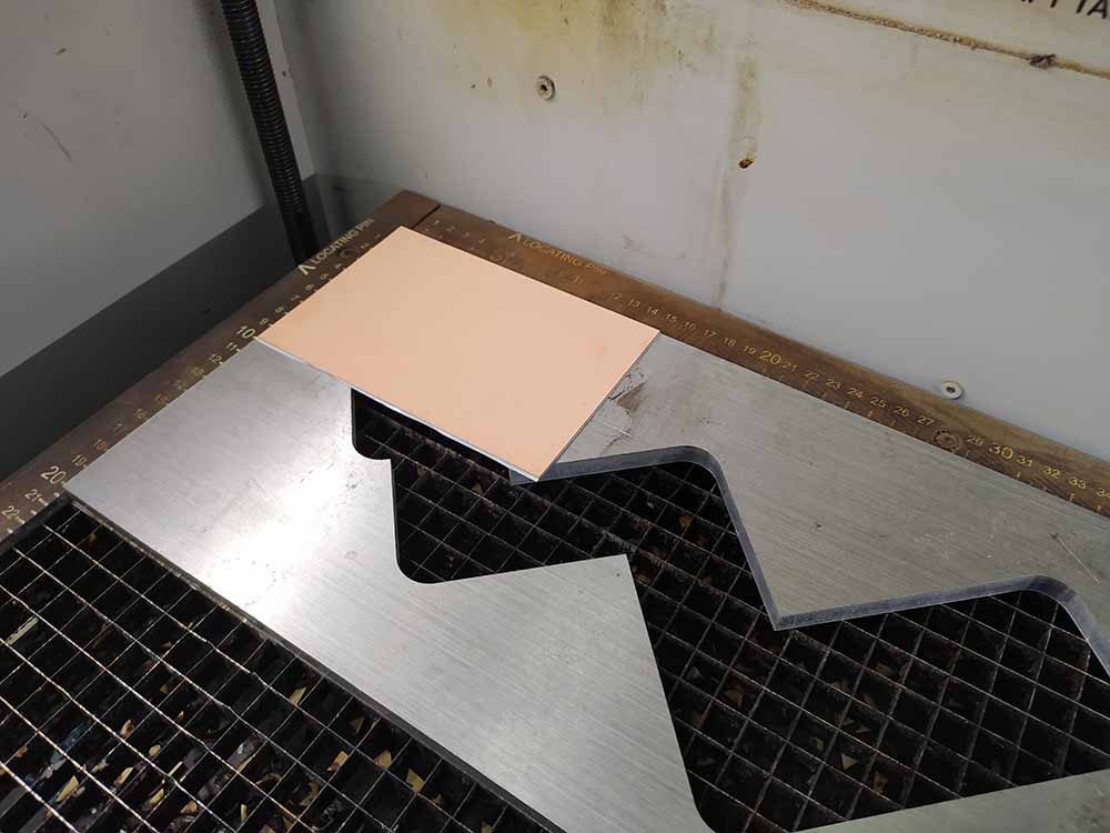
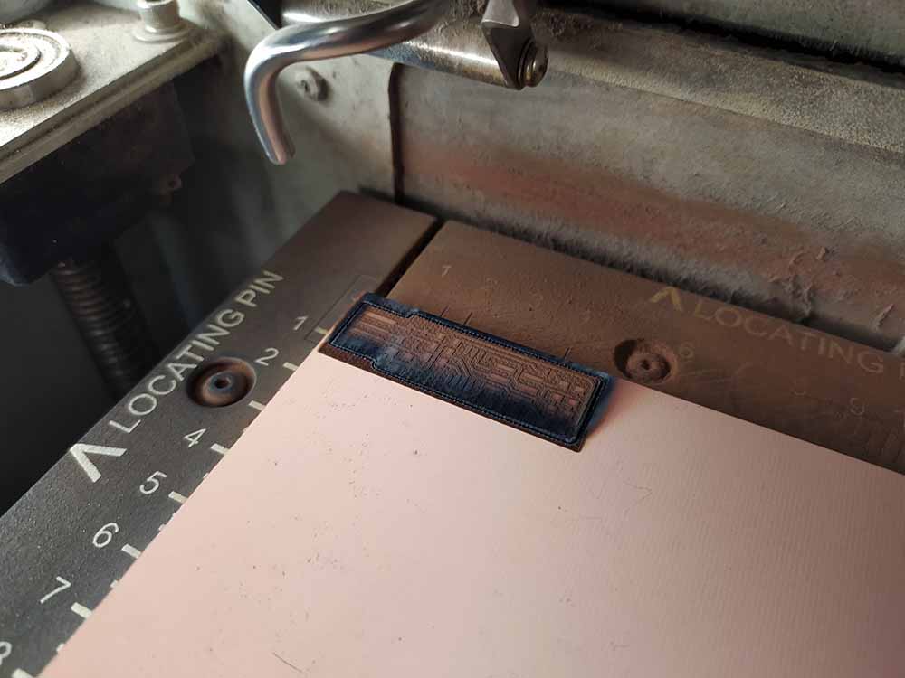
To prepare the copper board, I applied double sided tape to the bottom side of the board, and afixed the single-sided FR4 board to a slab of aluminum in the top left corner.
Here are the two strips of double sided tape placed side by side without overlaps and bubbles:
Here is the PCB taped onto the aluminum slap which we use as a cutting surface:
Set to the right focus for Fiber cutting:
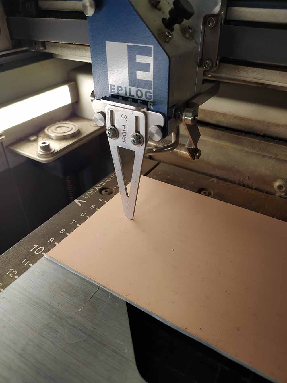
We want to see a nice blue/green light when the laser hits the copper. Once the board was engraved with the Fiber laser…
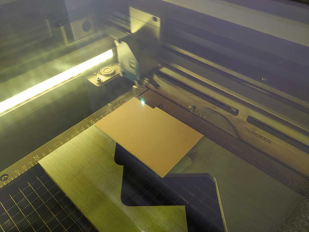
…I switched to the CO2 laser to cut out the board. I did about 12 passes. I knew when to stop when the laser got dimmer as it passed along the same path.
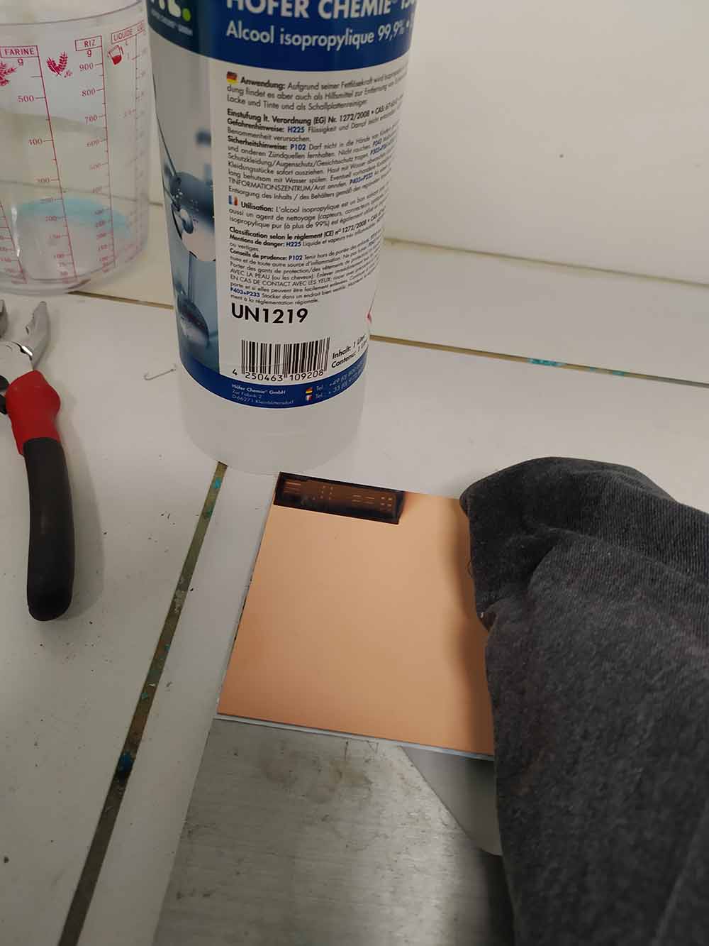
I rubbed the board with a rag and some rubbing alcohol to remove the soot. I am wearing protective gloves while doing this.
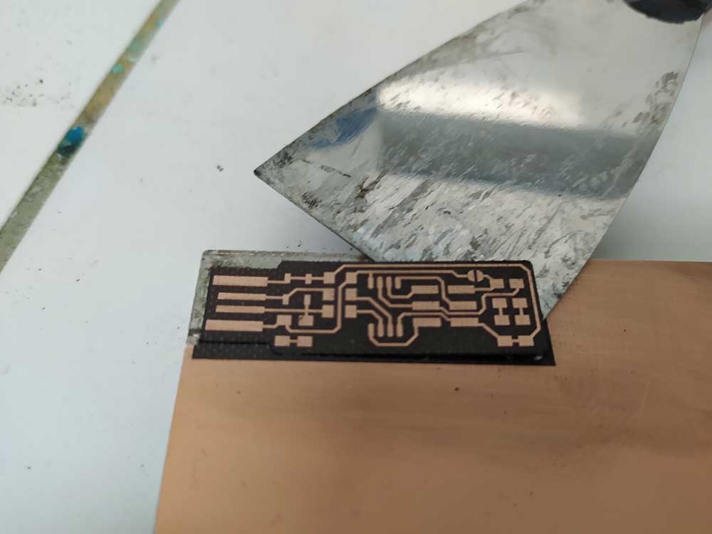
Removing the board sometimes requires retracing the cut line with an exacto knife…
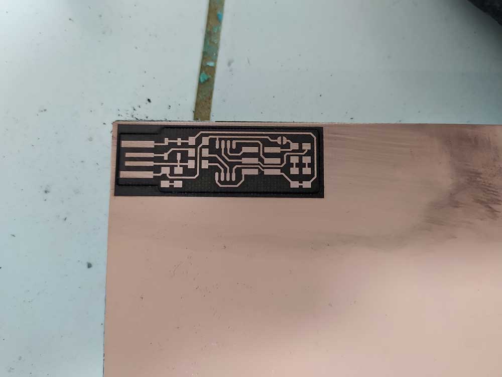
…but this time the cut was nice and clean.
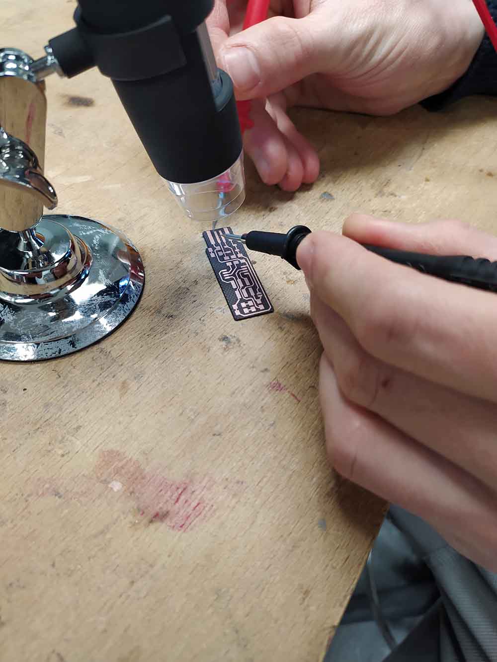
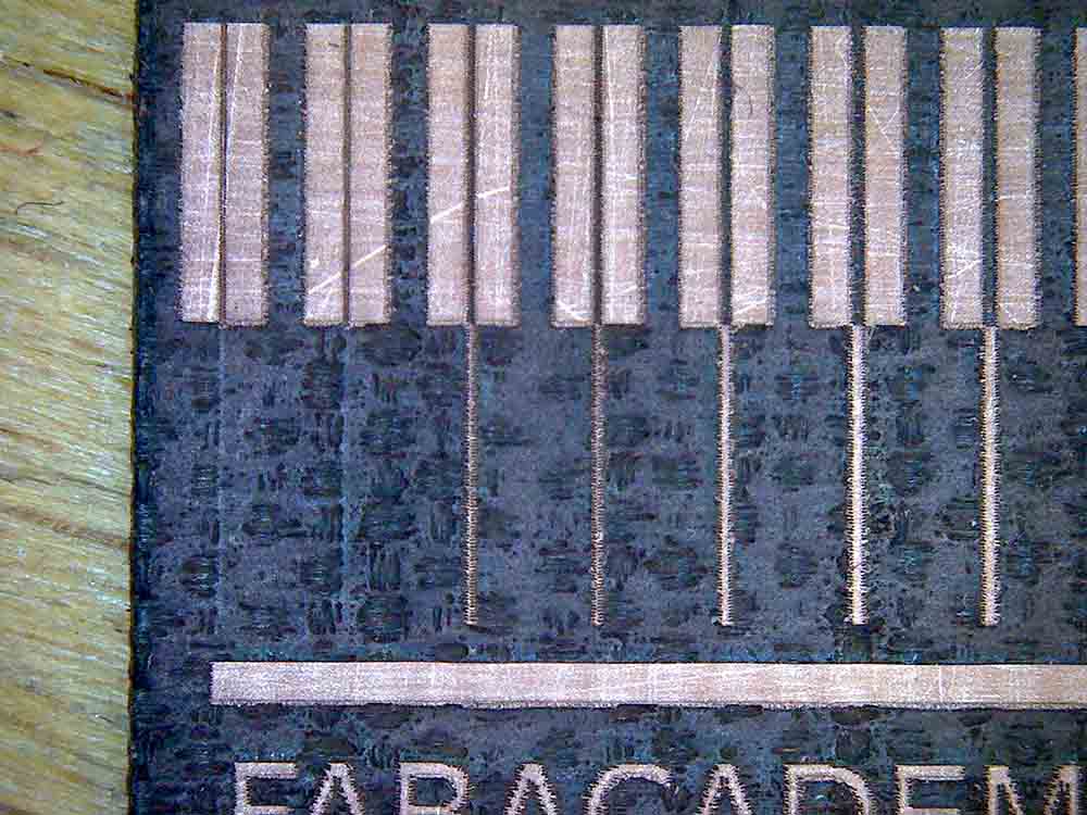
I then inspected the quality of the lasercut under the USB microscope, testing each connection with the multimeter in continuity mode and fine probes to make sure there were no shorts.Also to make sure that the wires I wanted to be continuous were in fact continuous.
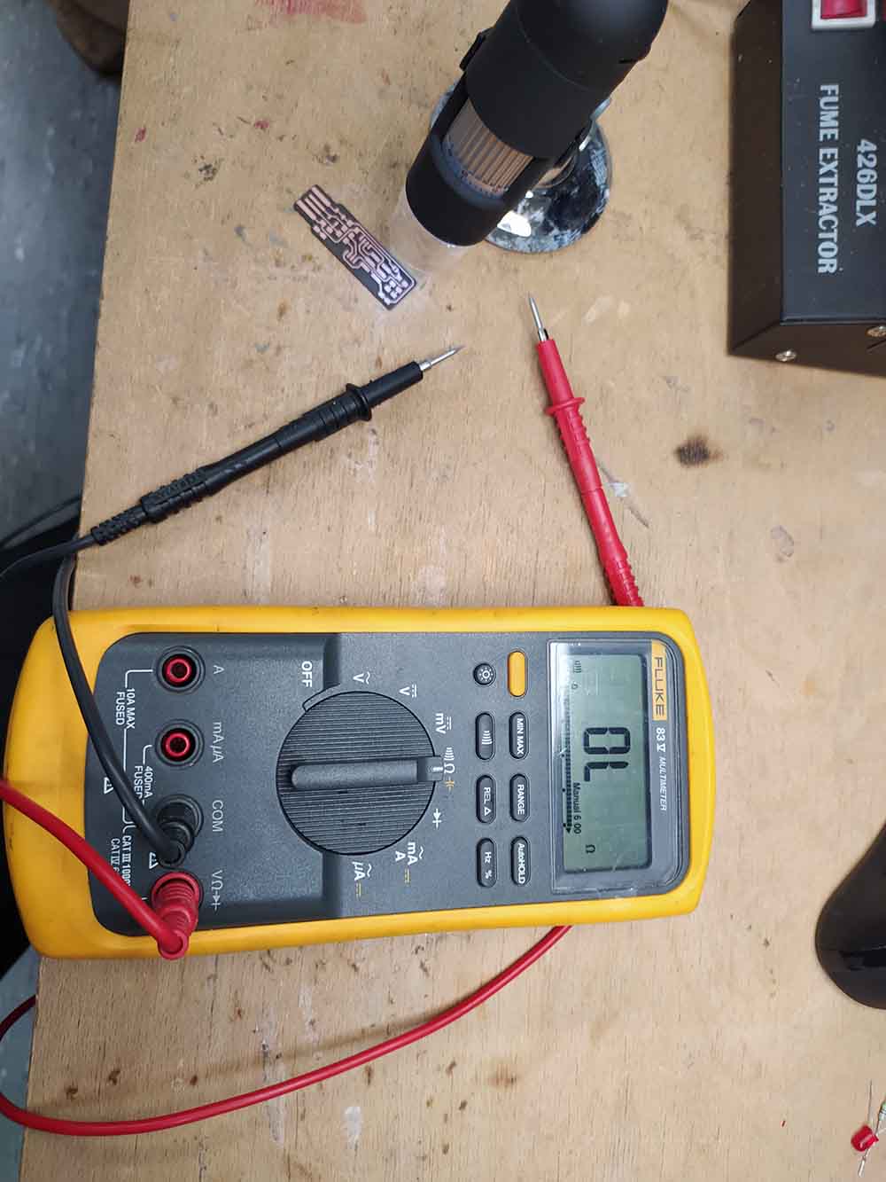
Here is what our setup looks like with the USB microscope and the probes:
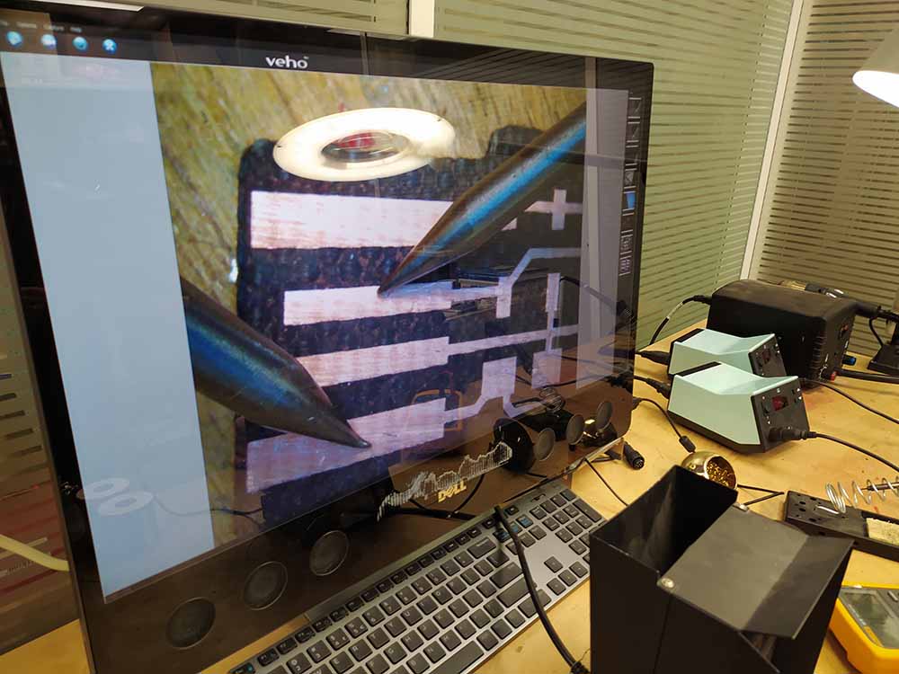
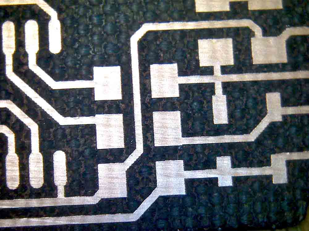
And here is the engraving quality:
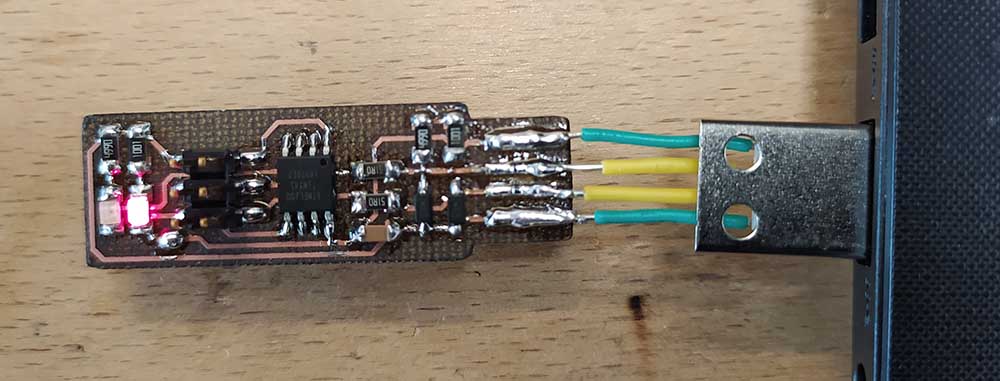
Fab ISP Electronics assembly
I then collected all the parts that I will be needing using a A4 piece of paper with double sided tape on it.
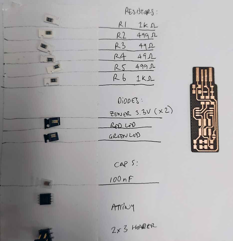
Despite this, I still accidentally included 49K resistors instead of 49R…
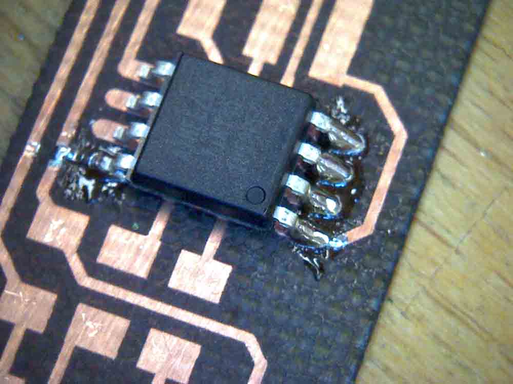
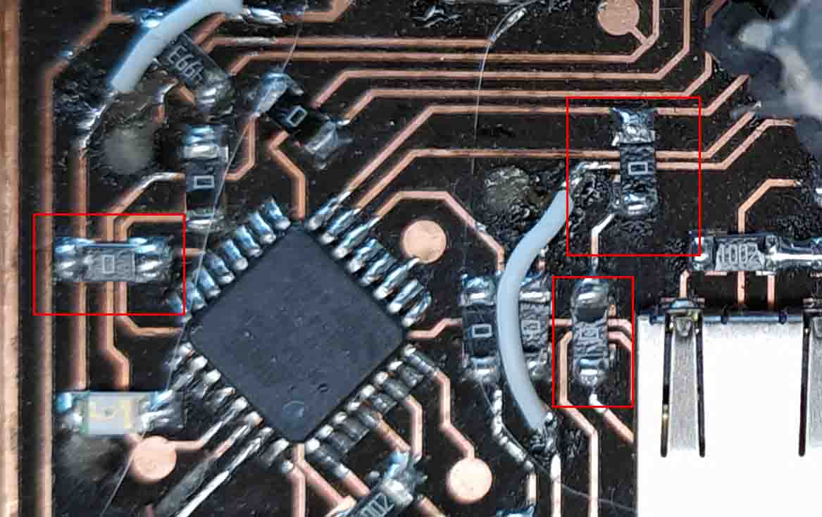
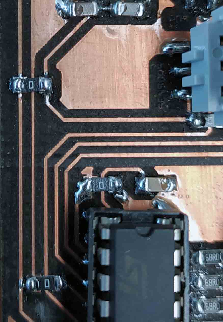
Here are some pictures from the USB microscope showing the quality (or lack there of!) of my soldering:
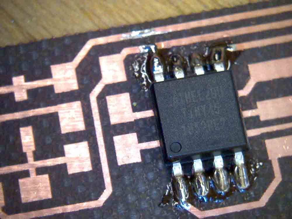
I started with the Attiny, as it is the smallest component and I didn’t want taller components getting in the way.
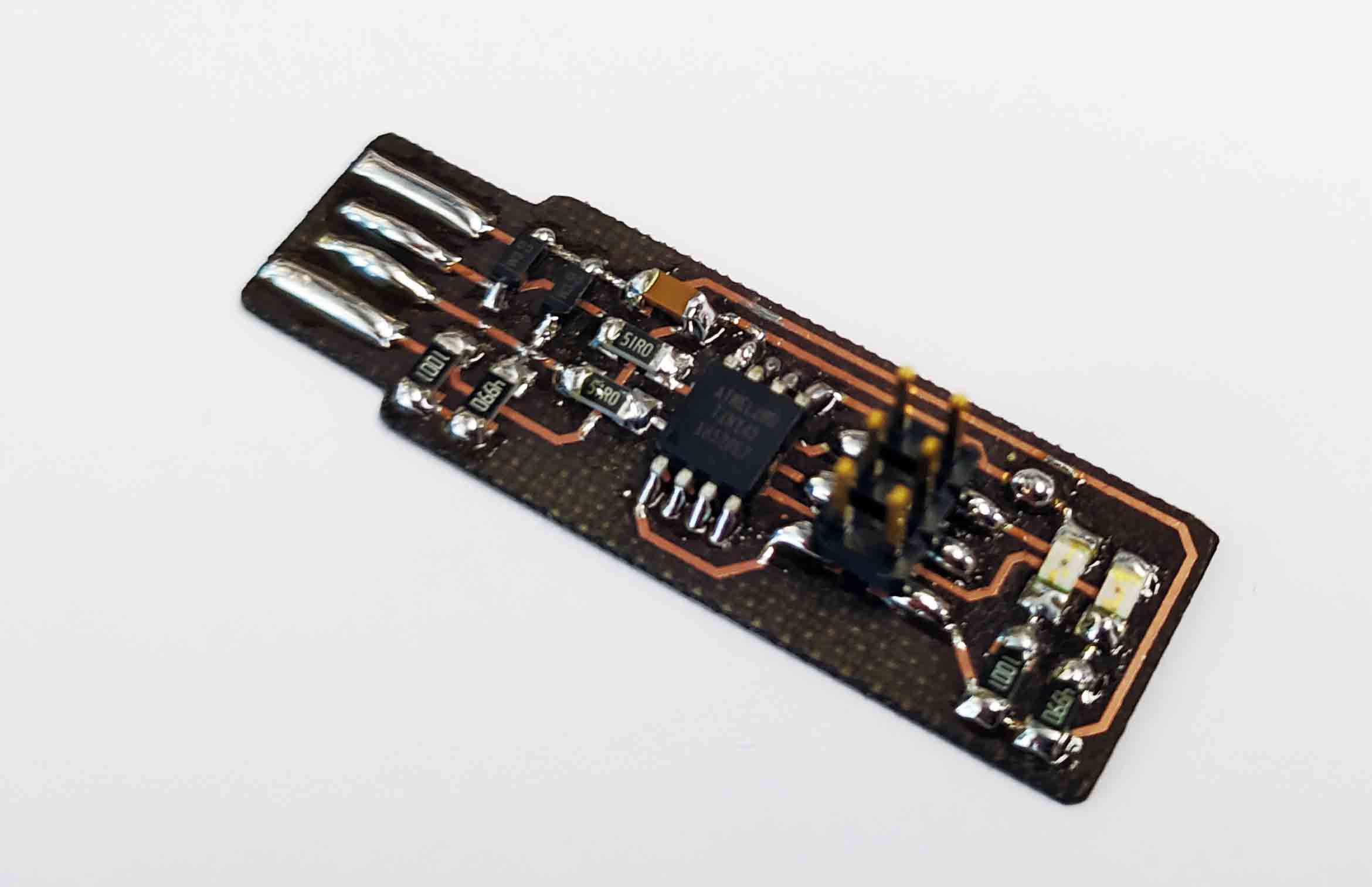
…and here is the final:
AVR Software download and toolchain setup
I’m using an Ubuntu laptop for this project. I first ran sudo apt install avrdude gcc-avr avr-libc make from the terminal.
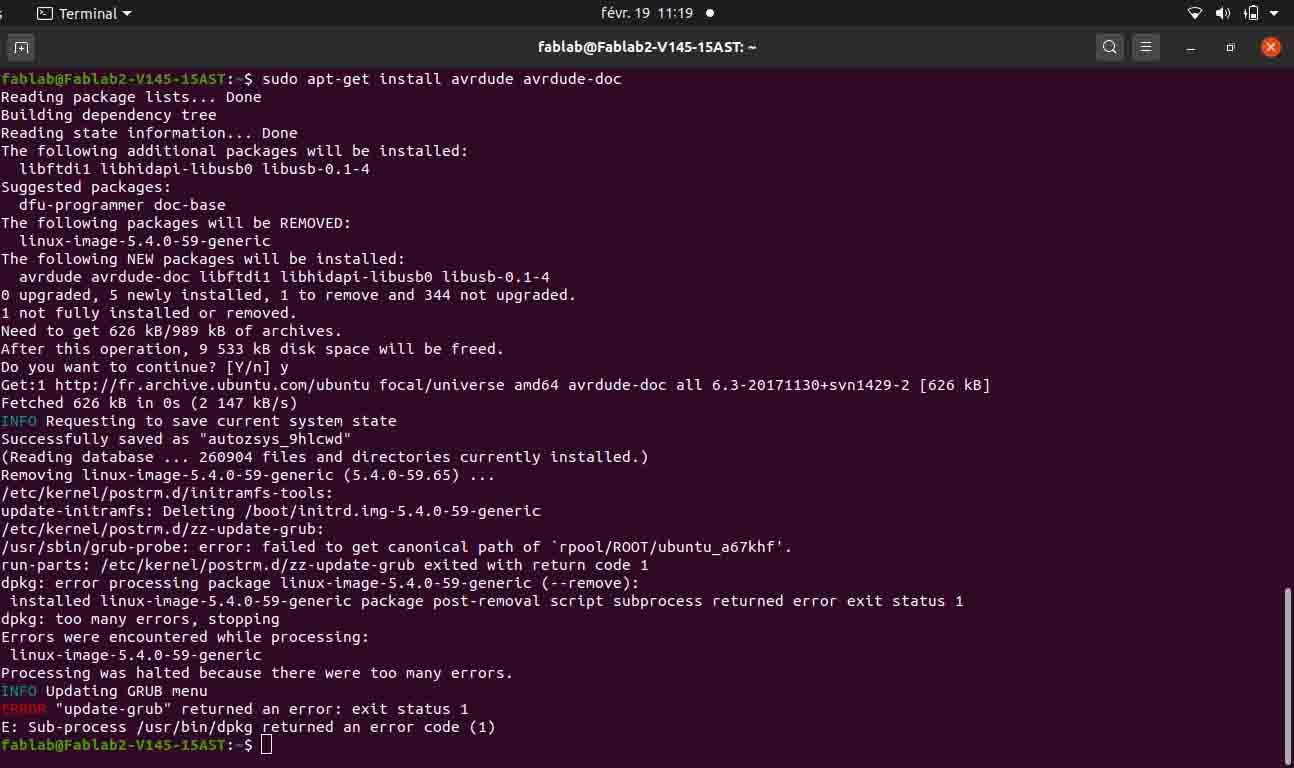
I am getting several errors but I am trying to see if it works just the same by downloading the firmware and trying to run “make”. Not working…
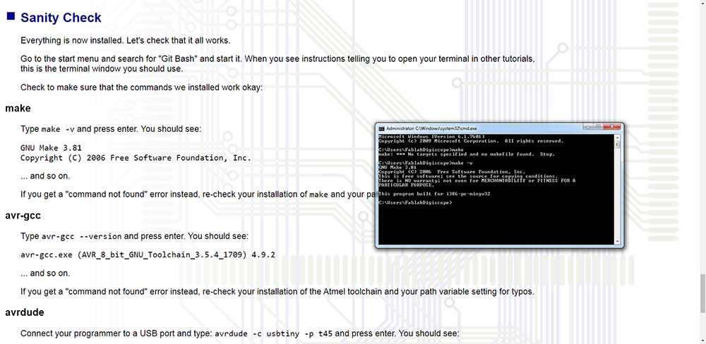
I switched to windows (!) and followed the installation instructions, they seem to be working:
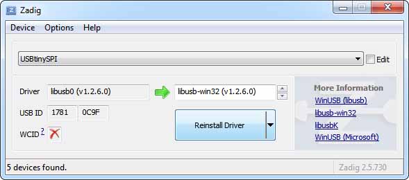
And the usbTiny drivers installed using Zadig:
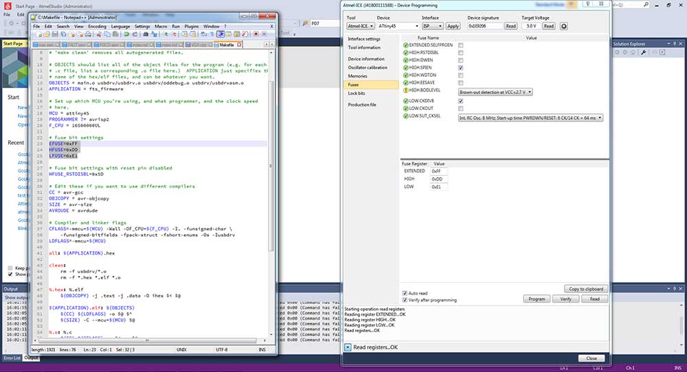
After installing AVRDUDE, I downloaded the firmware source code to the C: drive (as in the files are directly in the C: drive and not in a directory) and then edited the makefile in Notepad++ to reflect chip type and programmer:
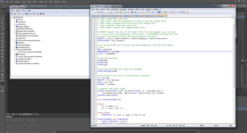
MCU = attiny45
PROGRAMMER ?= avrispv2 (I am using the white box with the blue stripe from Atmel)
F_CPU = 16500000UL
I then opened cmd.exe and typed cd\ (I put folder in C:)
I then typed “make” which will generate the hex. I got this confirmation:

I then powered the board with 5V with a power supply and typed “make flash”.This did not work as avrdude could not find the USB device.
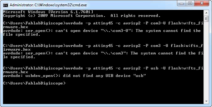
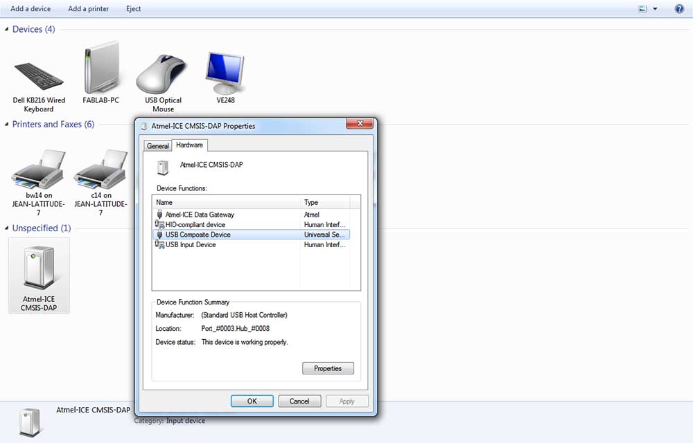
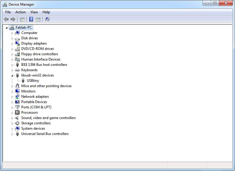
I tried various different ports, com 1, com 3, usb all did not work despite the Device Manager telling me that the device is on com 3.
I moved to Atmel Studio and selected the hex code generated by avrstudio located at C:
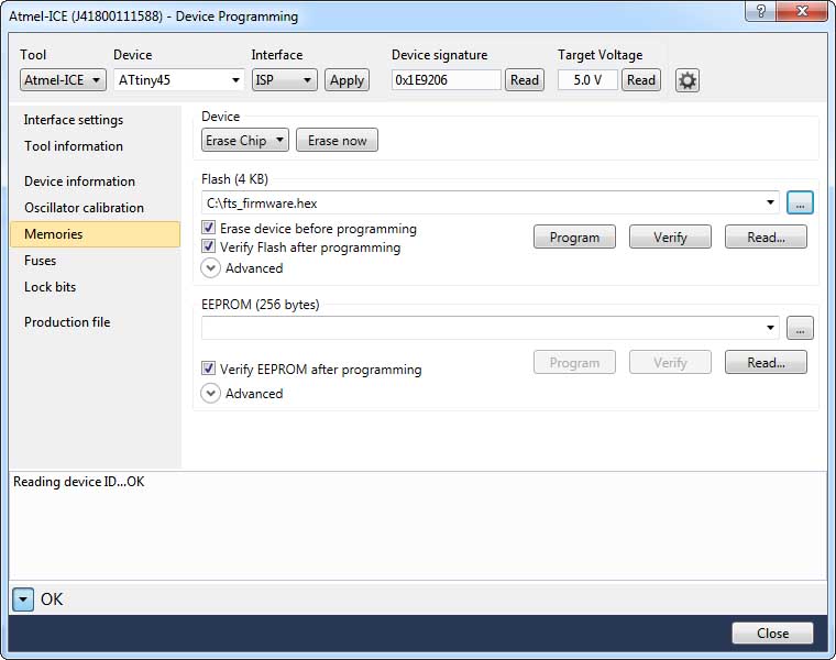
I am powering the target board and the red LED is coming on:
This appears to work fine. I then also burned the fuses (except reset disable) in Atmel Studio:
I tried plugging in the programmer to Windows and Ubuntu, I can see it under Device Manager listed as USBtiny in Windows and in Ubuntu with lsusb listed as Multible Vendors. Looking good!
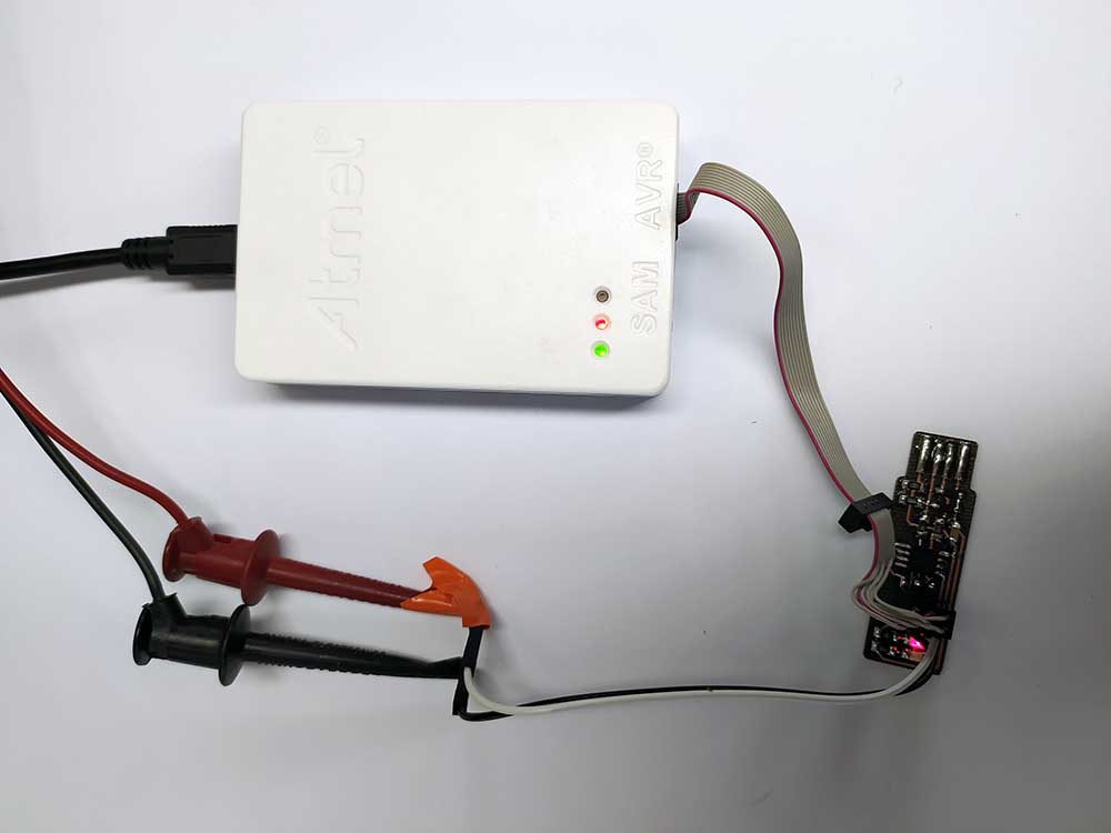
I then burned the final reset fuse in Atmel Studio and desoldered the bridge.
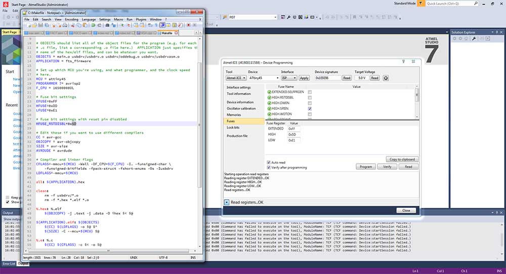
Ready to try to program something!
Programming something with the programmer
Making the programming header :
Because the pin 13 on the Arduino is PB5, I have a C code which just turns on and off PORTB.
#define F_CPU 8000000

#include <avr/io.h>
#include <util/delay.h>

int main(void)
{

  DDRB = 0b11111111; // PORTD is output


    while (1)
    {

PORTB = 0b11111111; // pins on
_delay_ms(1000);

PORTB = 0b00000000; // pins off
_delay_ms(1000);

    }
}
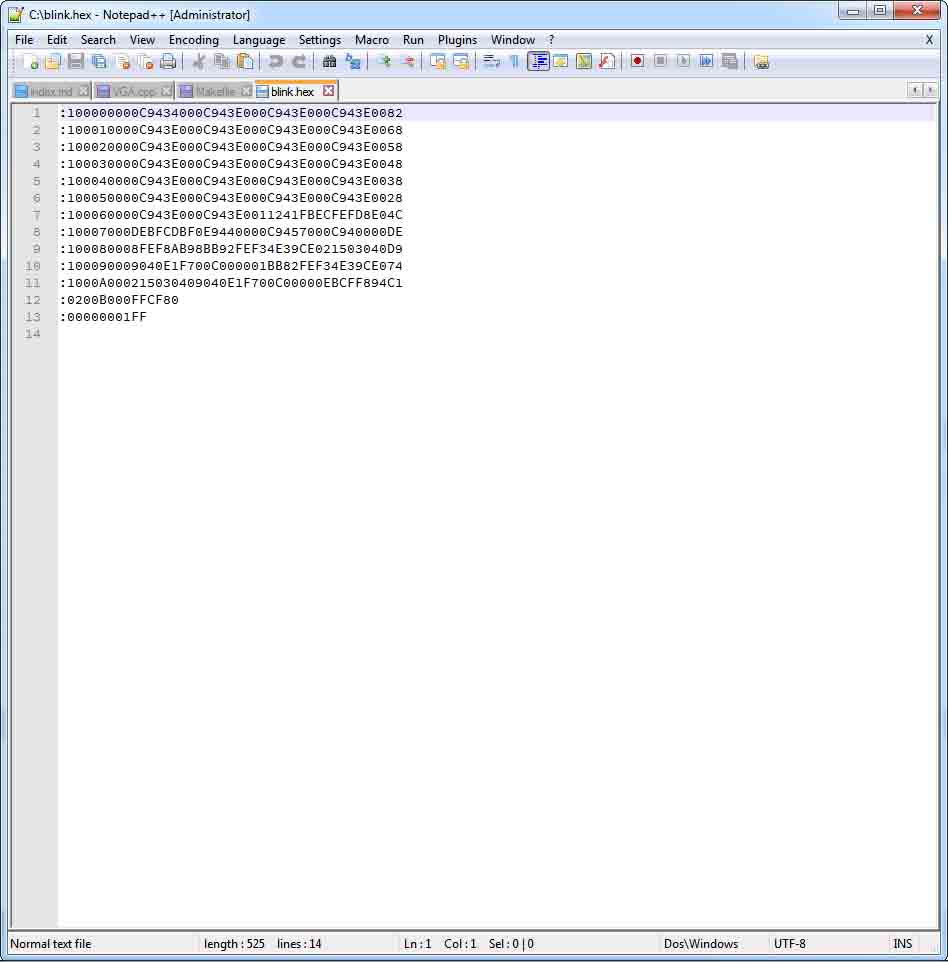
I saved this file as blink.c and then used make to turn it into a hex. Here is the resultant .hex file:
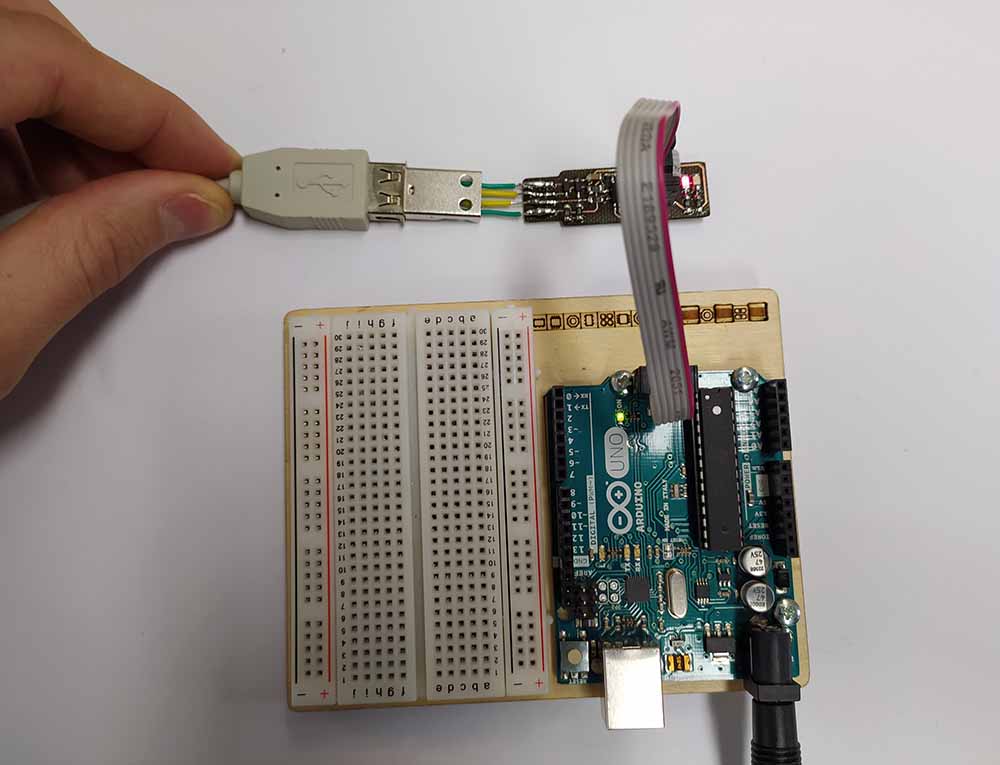
I plugged in the programmer to the ISP of the Arduino’s 328p (powered by a 12V adapter)…
I then ran the following command in avrdude (makefiles are cool but this is my preferred method): avrdude -c usbtiny -p m328p -P usb -U flash:w:blink.hex
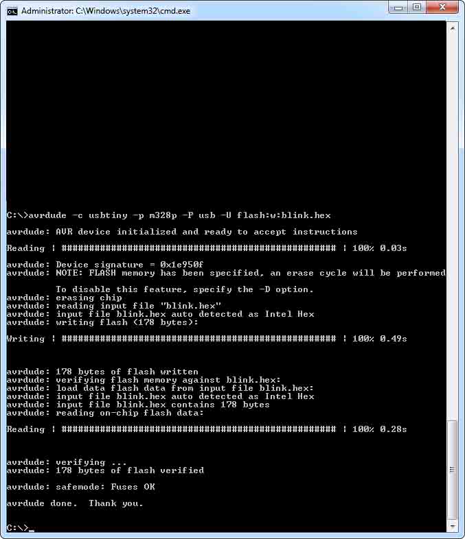
It appeared to successfully program and the arduino starts blinking on pin 13 once a second where before it was not blinking !
Group Project: Design rules for the laser PCB production process.
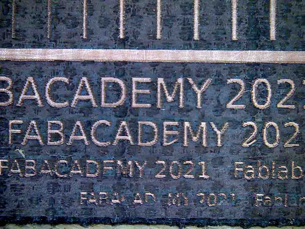
In order to explore the smallest features and text size possible with our Epilog Fusion M2 lasercutter, Ambroise and Selena developed a test image based on the fab academy circuit milling test file. We didn’t get the focus right the first time:
Selena recut the test board and took this microscope photos:
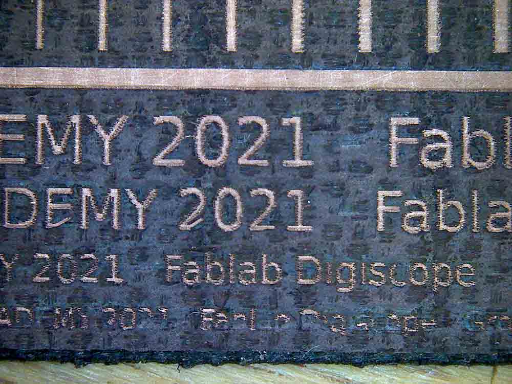
Clearly the cleaning process is responsible for removing some of the smaller copper features…
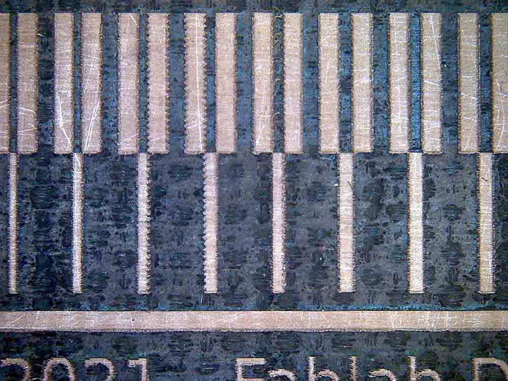
There is also a horizontal banding pattern which dissolves very fine lines…
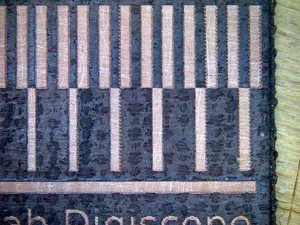
…and sometimes creates tiny shorts. This is why it’s important to test traces with the continuity tester!
While it is true that making holes and then putting rivets though on double sided boards is possible, we are mostly limited to single sided boards with SMD components on our laser cutter. It’s possible to squeeze two 0.4mm traces underneath a 1206 component…
… but I prefer to stick to one trace.
The machine’s focus is very important but once it is optimized the machine is capable of higher resolution that the Roland milling machines.
In terms of smallest components, the limit appears to be people’s soldering skills.
Once we get to the circuit design week we’ll go into more depth with setting up Design Rules (minimum trace widths, minimum distance between traces, etc.) in Eagle.