7. Electronics design
Assignment:
Individual: Redraw Eco Hello world board by adding at least one input.
Group: Use the test equipment to observe the operation of a microcontroller circuit board.
Individual Assignment:
PCB 1
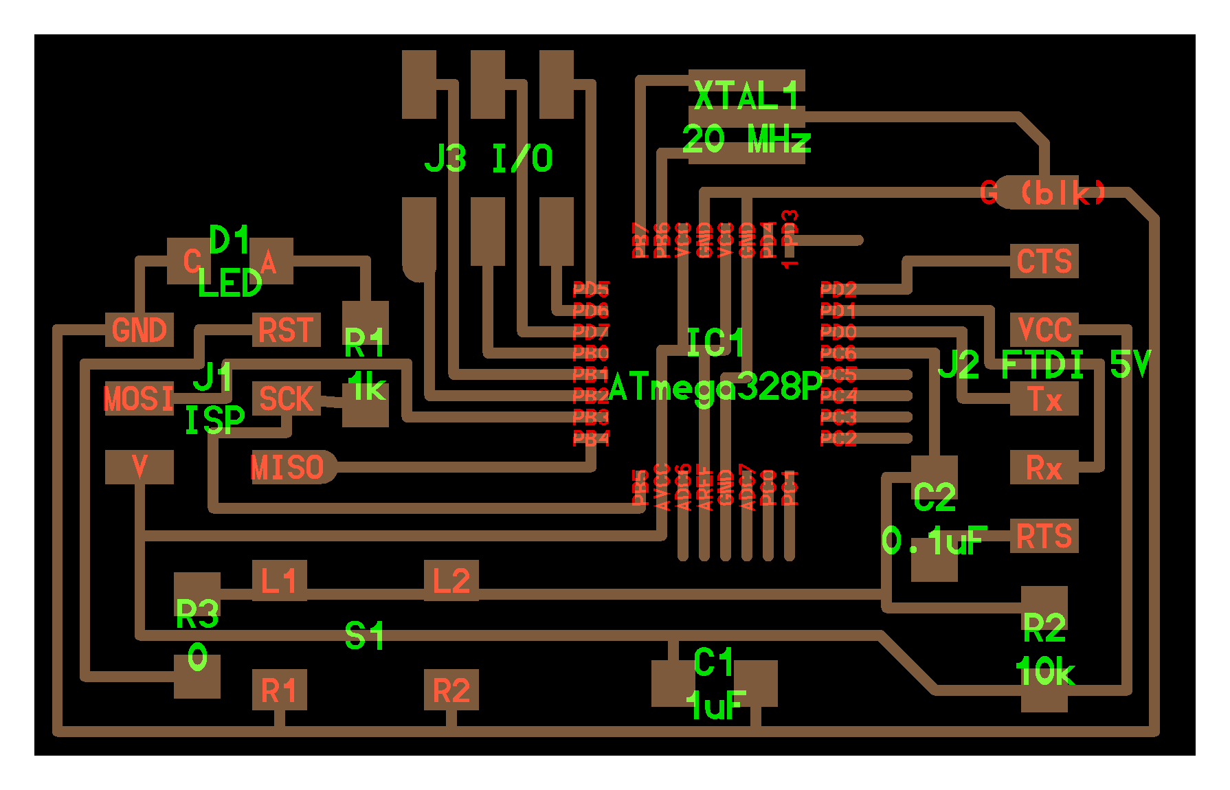
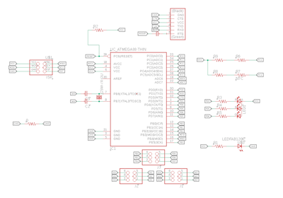
Our assignment this week was to design a PCB from the reference options listed in this, the PCB I chose was the ATTINY.328P. Part of the assignment was to add an input and output, so I added an RGB LED and thermistor, below is the thermistor circuit reference I used from the Fab Academy archive which I redesigned after integrating it to my board.
The first step was to download and install Eagle to create the circuit. I dowloaded the Fab components Eagle folder and added the folder in my eagle library. To do so, I opened the Eagle folder in Git and downloaded the fab file with .lbr extension. Afterwards, I opened my Eagle folder (where all relevant eagle folders are), opened the libraries folder, and moved the fab library (eagle_fab.lbr) to it. Make sure to move not copy the folder, otherwise it will not work.
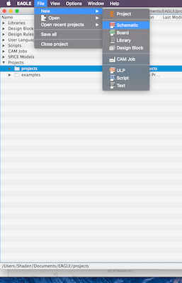
After installing, I created a new project schematic on Eagle:
Then I added all the components I needed. The components used in the ATTINY board were:
ATMEGA88 - ISP connector (2x3 header) - FTDI connector (1x6 header) - Resistor - LED - Capacitor - Crystal
Components I added:
RGB LED - Thermistor
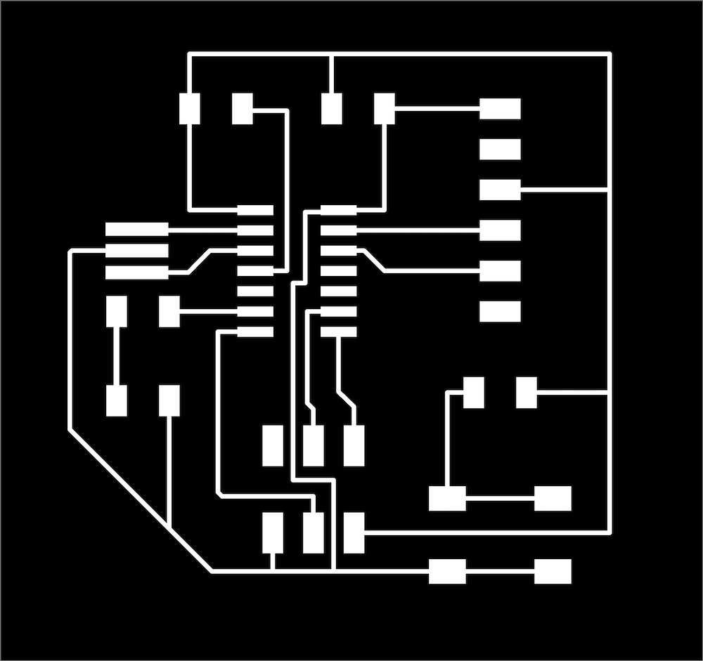
The image below shows my final schematic, after ensuring my connections are correct I converted the schematic to a board and started arranging the components.

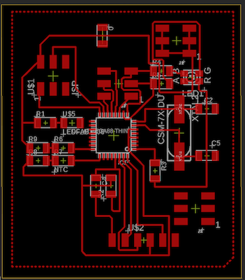
Board:
Before beginning the routing process, I change the clearance to 17ml (to match the CNC bit size and settings).
![]()
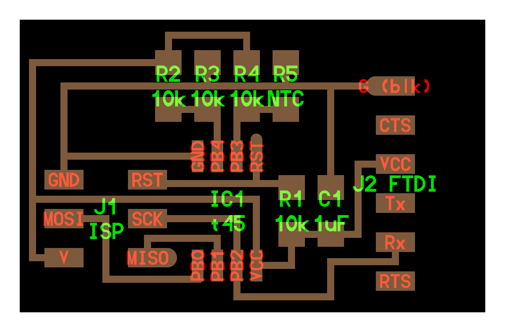
Below is my final board:
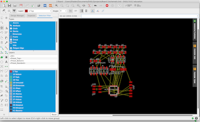
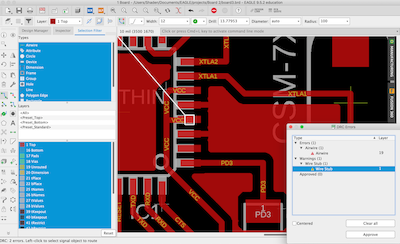
I then ran an error check (DRC) and fixed the errors I had.
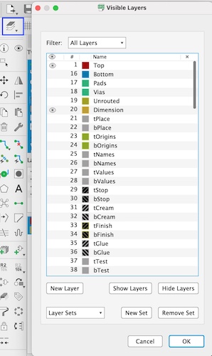
To export the final file, I first opened the layer panel and hid all the layers except for the top layer and dimensions. Otherwise, Eagle will save the file with all the labels and that will result in the these parts being milled as well.
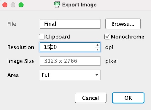
To export go to file > export > image and select monochromatic, increase the resolution to the highest possible, name and export your file as a PNG.
I imported the PNG file in Fabmodules to prepare the Gcode file. The next step was to prepare the machine for milling. Please refer to the Electronics Production assignment for both processes.
Below is the image of the board, there were a lot of errors here. I unfortunately wasn’t able to finish it because the lab was closed. However, the next section will take you through my process to create the Eco Hello world board.
PCB 2
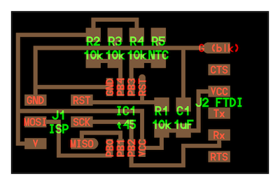
After getting back in the lab, I decided to work on the Eco Hello World board instead. The components are:
- ATTiny4
- 1 2x3 pin-Header
- 2 10Ω Resistor
- 1 499Ω Resistor
- 1 uF Capacitor
- 1 6 pin-Header-Male
- 1 6 SMD
- 1 Button
- 1 LED
- XTAL Resonator
I followed the same steps as above and exported the final PNG file:
Milling
In the new lab I was using another machine (Carvey Milling) so the software and the process was different. Carvey was much more user friendly to use, the software Easel was also much easier to use than fab modules, and also gave more room for editing in the program. For example, I created the outline in Easel instead of Illustrator. After downloading the program, I began the process of prepping my files.
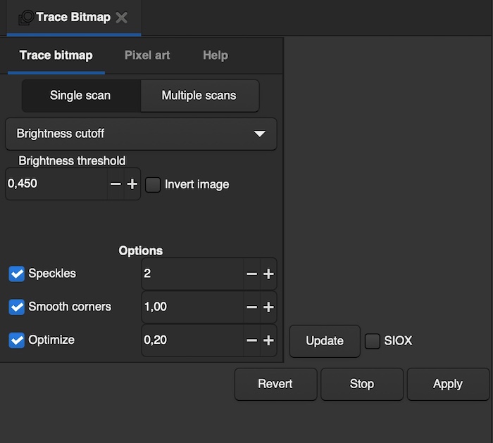
The first step is to open the PNG file in Inkscape and convert it from a raster image to a vector image using the trace bitmap option.
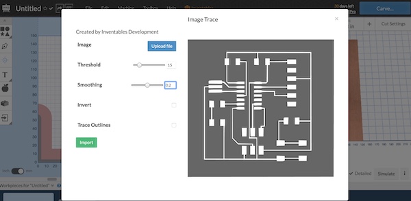
Once the image is converted, I exported it to a PNG and opened it in Easel. The first step was to open a new project in Easel, the select import, image trace, then select the file. I then input the below values.
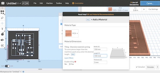
I then selected my material (PCB), and input the dimensions.
Two issues came up here, because I am using a Macbook, the image was doubled in size. After looking at previous students experiences with this, I found that the way to solve this is to resize manually using preview, illustrator, or Inkscape. I tried all three options but it didn’t really help. The solution was to resize in Easel by changing the dimensions manually in the shape tab to the exact board dimensions I got from Eagle (as seen in the image below). If you’re using Mac, I recommend making sure your board dimensions are rounded (40, 41, 42, etc) so the resizing can be done without compromising the final outcome. The second issue I faced was the width of the material, the width I put in was 5mm, but it was 1.7mm -big difference. I relied too much on previous students documentation without doing measurements myself, which resulted in the bit breaking when I cut the outline at a later point.
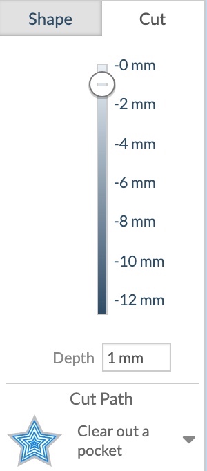
For the feed and plunge rate, I input the below values as per my instructors recommendations. I selected the pass depth as 0.1 mm, and set the total cut depth to 1mm.
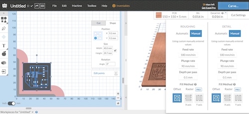
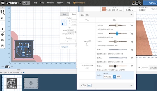
I selected the custom bit and input the dimensions (1/64) for carving.
When I did the time estimation it came to 11 hours, which was unnecessarily long given the size of my board. After looking at some online sources and discussing with my instructors, Yousef recommended I change the cut depth to .1mm and the pass depth to .1mm as well. This changed the total time to 44 minutes with the same results! The pass depth refers to the depth each round of cutting will go, so if your total depth is 1mm and pass depth is .1mm, you will end up with 10 passes total resulting in the extra time.
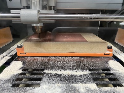
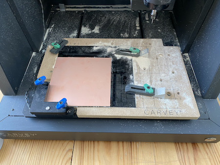
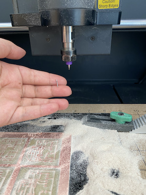
To begin carving, I set up the machine by placing a new PCB sheet with double sided tape, then securing the clamps really well. To insert the 1/64 carving bit, I used two wrenches to secure the bit by moving one clock wise, and the other counter clock wise.
I then went back to Easel, and started the carving process by clicking the Carve button on the top right of the screen. After finishing the first carve, I noticed that the bit wasn’t carving certain parts as seen in the reference image below. We tried many options; changing the threshold, redoing the board layout on Eagle using a Windows operated laptop, and adjusting some parts manually on Inkscape. The solution that gave the best result and was most recommended was to edit manually on Inkscape, however, I felt like that was too complicated and that surely there was a solution to this.

After a week of trying and many failed attempts, I found this previous student’s page who recommended using SVG instead of PNG. I learned from this experience to always look and as many pages documenting the same process using the same machine to avoid wasting time! I was finally able to carve a couple of PCB’s then proceeded with cutting the outline.
I created an outline using the pen tool, and made sure it’s on the same axis (X,Y) and dimensions as the board. I then changed the bit settings to cutting at 1/32 inches. I changed the cut depth to the material depth (1.7mm). As I mentioned earlier, the first attempt was with a 5mm cut depth, that immediately broke the bit as seen in the second image below.
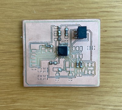
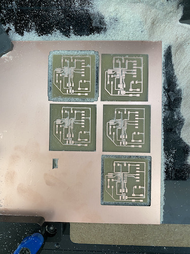
Final PCB on the bottom right:
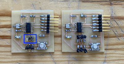
Moving to soldering, I started with the centre parts and moved outwards. For more details on soldering you can refer to my Electronics Production page.
I had to solder my board twice, when I came back to the lab the next day I found one of the pins had ripper from the board. I believe it happened by mistake during regular lab cleaning. The pin in the second board also ripped when I connected the wires to the pint and tried to take remove the wire! I had to leave the lab and didn’t have time to cut again and solder as well, so I cut the PCB’s and will solder once back in the lab tomorrow. Overall, soldering is a skill that can be mastered with time, and I’m still working on it!
Programming:
To program my board, I will be using arduino as an ISP. I followed this as well as Nora’s and Munzir’s process for programming their board.
The first step was to connect the pins as follows:
- Arduino Pin 13 —> SCK
- Arduino Pin 12 —> MISO
- Arduino Pin 11 —> MOSI
- Arduino Pin 10 —> RESET
- Arduino 5V —> VCC
- Arduino Ground —> GND
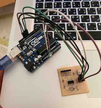
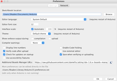
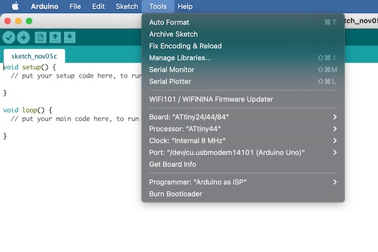
I connected the USB and opened Arduino to add Attiny to the board library. Go to File > Preferences.
At the bottom of the pop up menu where you see “Additional Boards Manager URLs” you want to copy and paste “https://raw.githubusercontent.com/damellis/attiny/ide-1.6.x-boards-manager/package_damellis_attiny_index.json” (without the quotation marks) and click OK.
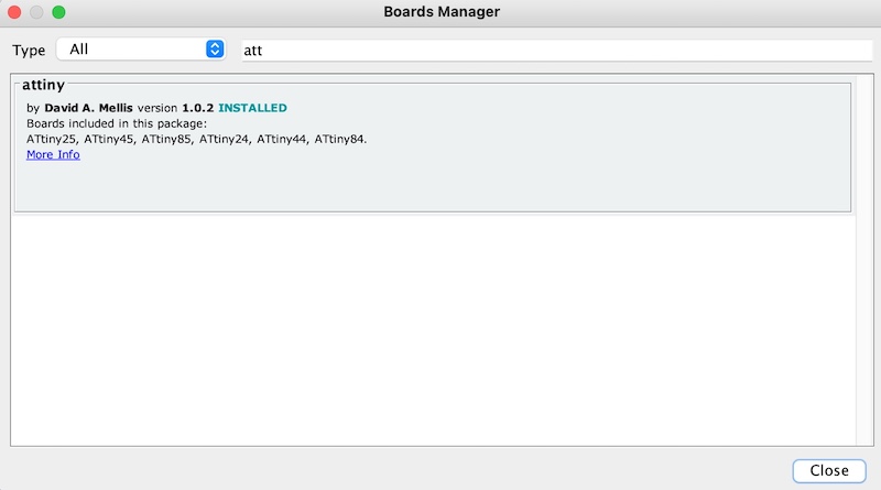
Navigate to Tools > Board > Board Manager. At the bottom and you should find “attiny” - you can also use the search tab. Click the install button and the words “Installed” should appear when the task is complete.
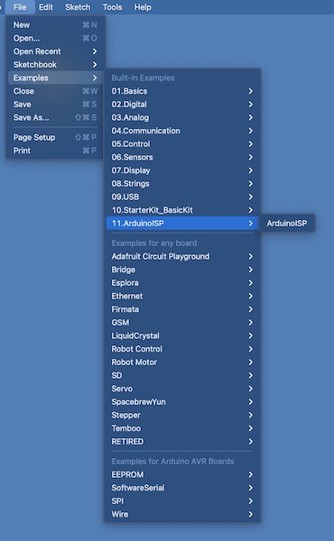
Then go to File > Examples > ArduinoISP and a window with code should open
Then go to tools > board > attiny 24/44/48. Under processor select attiny 44. Clock should be at 8mhz (internal attiny clock). Then select your port.
Then select “burn bootloader” under tools. This is where I received the error message “programmer not responding” - I wasn’t sure what the issue here was, so I changed the clock to 20 MHZ to see if that would make a difference but I still got the same error message.
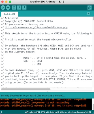
I double checked the direction of my soldered microcontroller and it was correct, I also double checked the pins and all were correct. I restarted Arduino and followed Nora’s process instead of the tutorial. She did not burn the bootloader and instead uploaded the Blink code directly, I changed the void loop and void setup but still got the same error message.
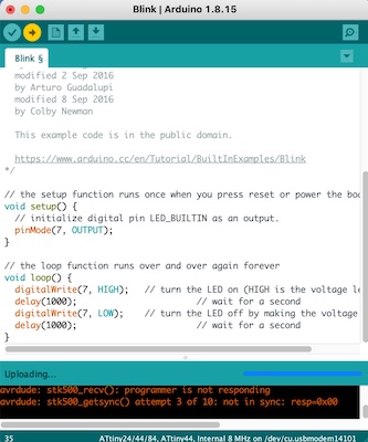
The only reason I could think of is maybe because I used male to male jumper wires and cut one side with pliers to make it female, and that probably compromised the connection. I will be back in the lab tomorrow and check with male to female and hopefully that is the only issue!