4. Electronics production
Group assignment
● characterize the design rules for your PCB production process
Individual assignment
● make an in-circuit programmer by milling and stuffing the PCB, test it, then optionally try other PCB processes
Group assignment
Group:
● - Xinhui Hu
● - Zhengya Gong
● - Yazan Barhoush
● - Noora Nyberg
The details of group assignment
Individual assignment
PCB Milling Process
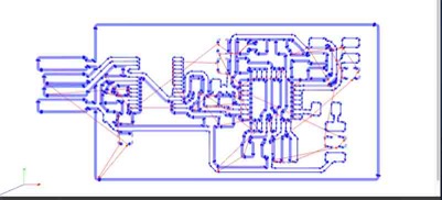
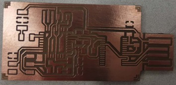
Of the lecturer suggested on the Fab Academy’s talk page this week, I chose the version from - Fab Lab Oulu.Also, most of Fab Academy students from Fab Lab Oulu did the same thing. So, if I run into problems, I will get excellent support. Fab Lab Oulu provided the .png files required for PCB traces and cutout borders on his page. Therefore, I need to make a .rmf file for the SRM-20 milling machine.
Making the .rml file:
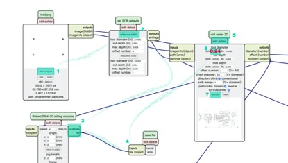
Antti gave a comprehensive lecture on the subject, including how to convert the .png files to .rml using mods SRM-20 machine, etc.
● Go to - Mods
● Select png file and press invert.
● Select the process from process > PCB traces (1/64).
● Select SRM-20 as the milling machine. Set the speed to 4mm/s and origin (x0, y0, z0) to zero and outputs to inputs.
● Set the tool diameter (I used a 0.23mm flat milling tool), the cut depth to 0.1016mm, the offset number 5 needed to clear the copper between USB pins, offset stepover number to 0.5.
● Press the calculate button. Now save the .rml file.
For producing the other file, the process is more or less the same.
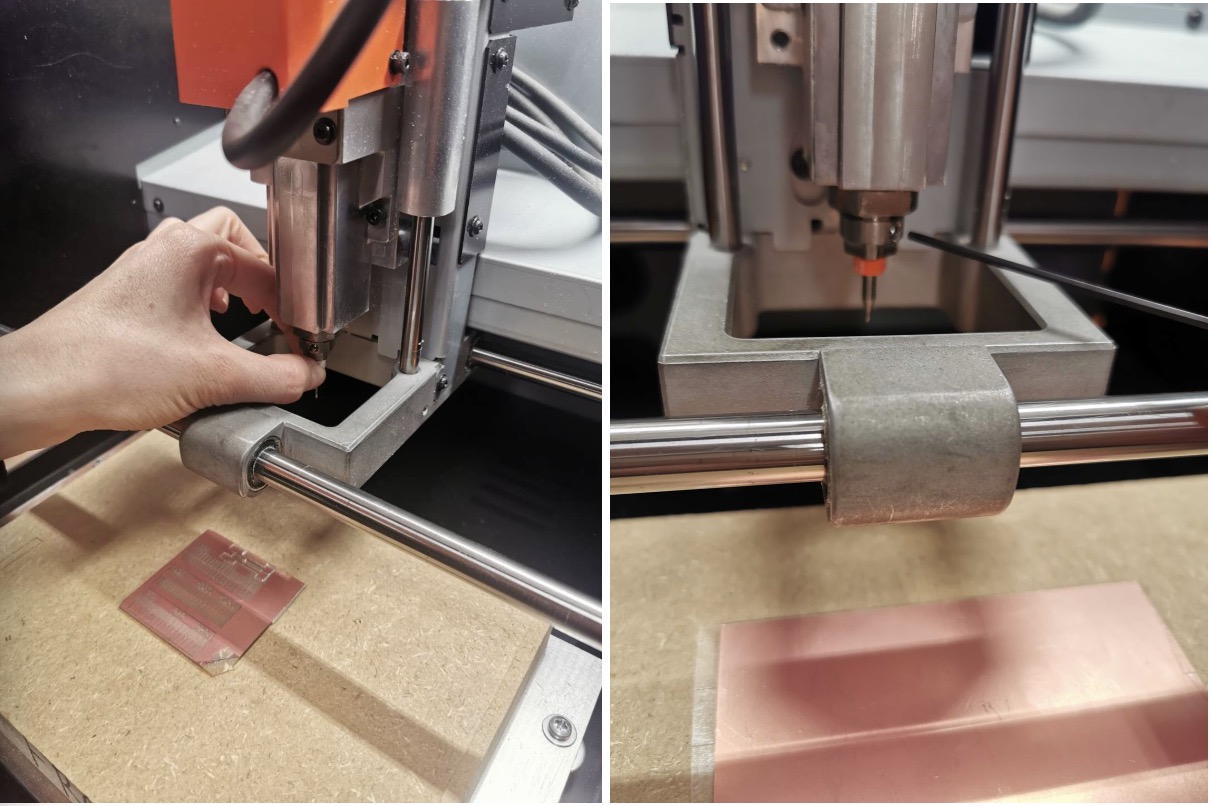
Milling the PCB:
The process is same as the group assignment.
We used a Roland SRM-20 milling machine to engrave the test patterns on the PCB board via VPanel software.
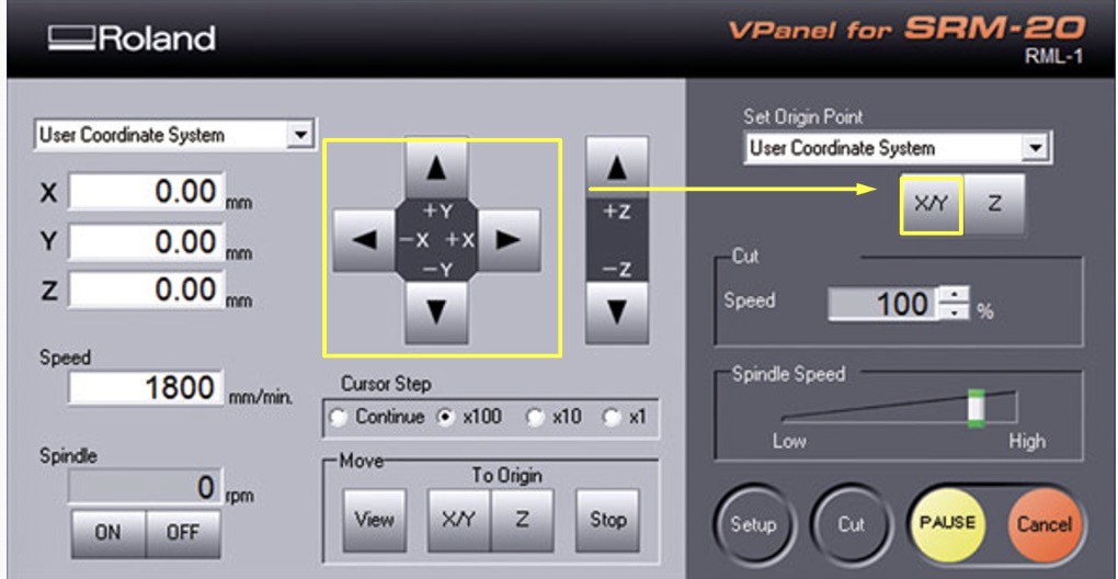
Calibration:
Adjust X/Y origin: The X/Y origin determines the start point on the flat PCB board. The X/Y direction buttons can be used to adjust the X and Y coordination of the milling bit. After reaching the ideal location, click Set Origin Point >> X/Y to set the current coordination as X/Y origin.
Adjust Z origin Z coordination determines the depth of the milling bit.
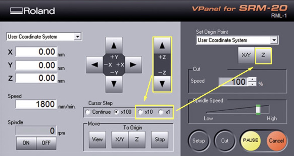
● Use the Z direction button to lower the milling bit until it is close to the PCB board without touching it. Select a small cursor step when the milling bit comes close to the board.
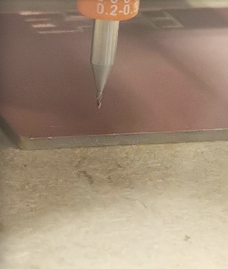
● Hold the milling bit with one hand and use the hex key tool to gently release it with the other hand. Carefully let the tip of the milling bit touch the surface of the board and fasten it again.
● Click Set Origin Point >> Z to set the current height as the Z origin.
Calibration
For V-shape milling bit, it is necessary to calibrate how deep it cuts into the board. Rise Z for 0.3 mm and set the location as the new Origin Point of Z and test the cut depth with the rml files saved from mods.
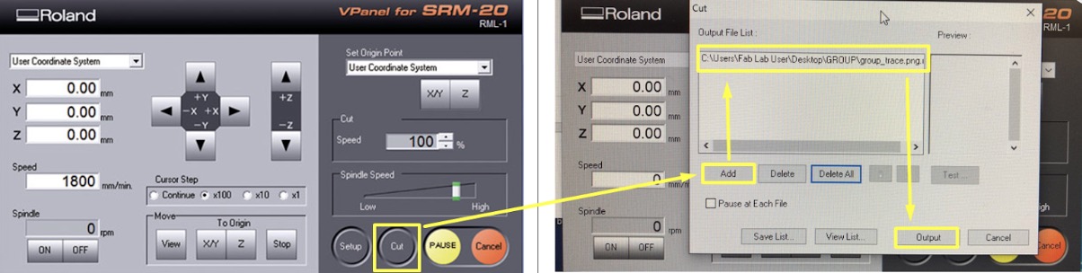
● Start the cutting task by Cut >> Add >> Select corresponding file >> Output. (The cutting task will start immediately after clicking “Output”, please double check everything before that).
● Pause and Cancel the task if milling bit is not touching the PCB board, which is expected to happen in the early rounds of calibration. In order to recalibrate, Click View >> To Origin >> Z to bring the milling bit back to its previous position. The order here is very important. Users must click “View” (which will bring the board forward) before clicking “To Origin Z”, otherwise the milling bit may be broken.
● Use the Z direction button to further decrease the height of the milling bit by a small amount, reset Z origin and restart the test task. Repeat the routine until the milling bit cuts into the PCB board with appropriate depth. This depth will be set as the final origin of Z for this milling task.
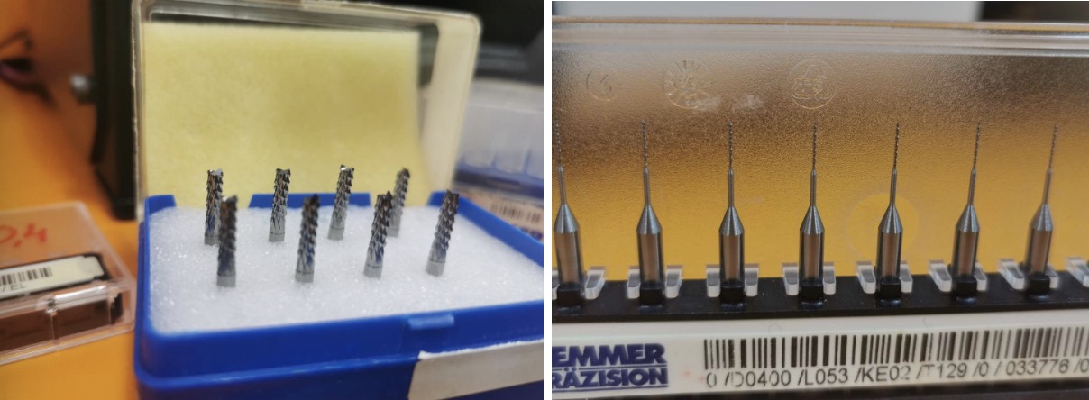
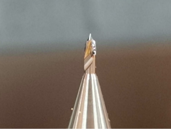
Milling bits:
● Select milling bits
There are many different sizes of the milling bits, for the inside milling, usually using the 0.2mm-0.5 mm V milling bit size as the figure. Also, we were cutting the outline using the 1.0mm size.
● Connect Milling bits
To connect the cutter, hold Milling bits between our fingers and insert it in the place. Then use a hex wrench to tighten it.
● Loosen the Milling bits
When we had been set up the XYZ, we need to loosen the Milling bits shown as figure.
Then cut it and waiting.
Soldering the Components
● Using the components list to find the components
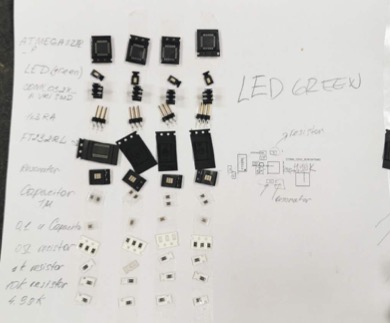
● According to the image of - Noora Nyberg’s version, to soldering it.
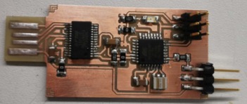
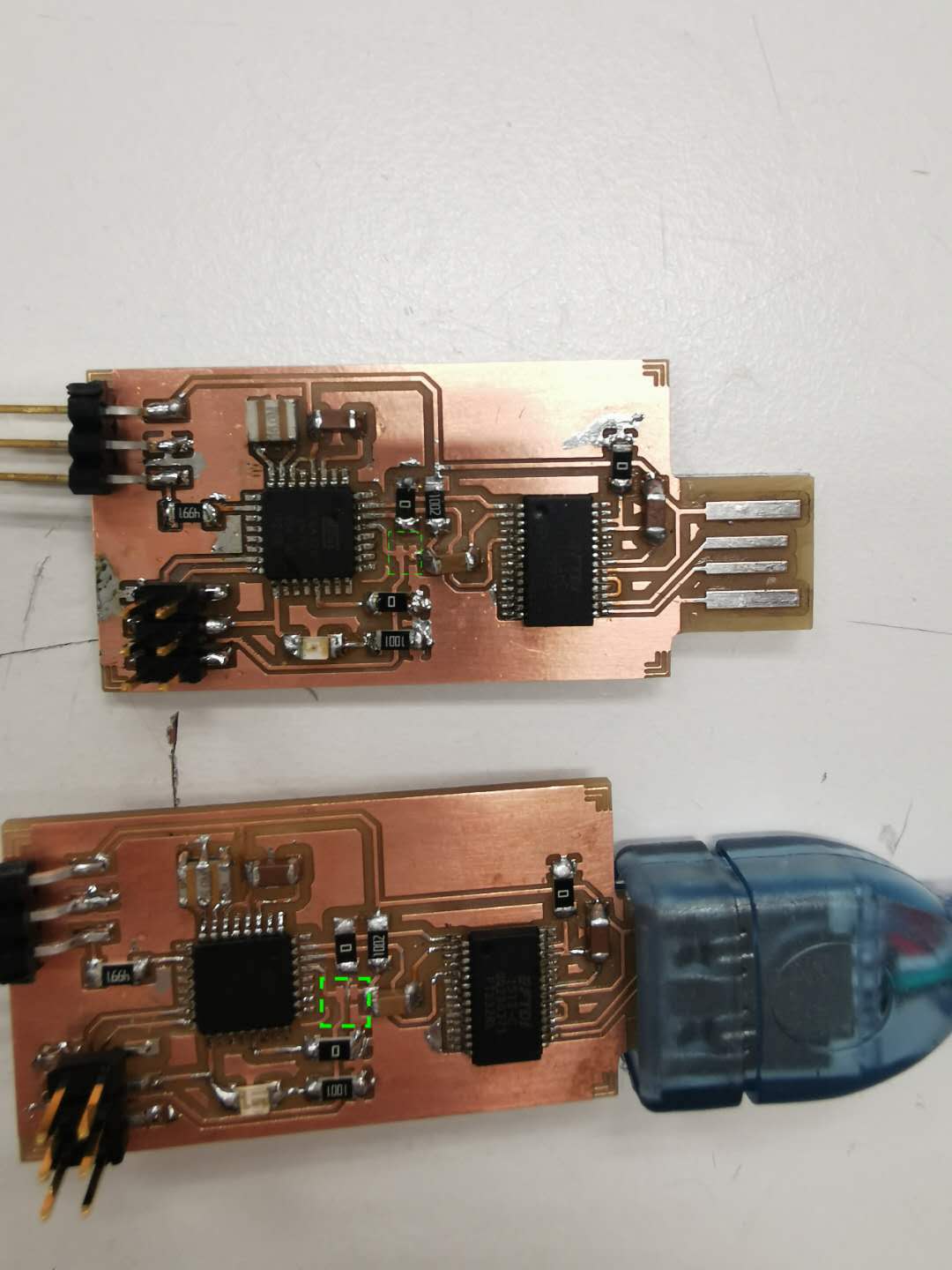
● The first PCB board. Because of my carelessness, although Gleb helps me fix it, the first PCB is very uglily, and I do not want to see it again.
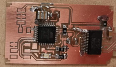
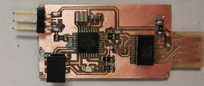
● The second PCB board is not very good, but when compared with the first one, it is perfect.
Programming
Preparation :
● Pasting several layers of tape on the back of the USB port to make it more suitable for insertion
● Downloading the Arduino and the -UPDI programmer sketch
Programming
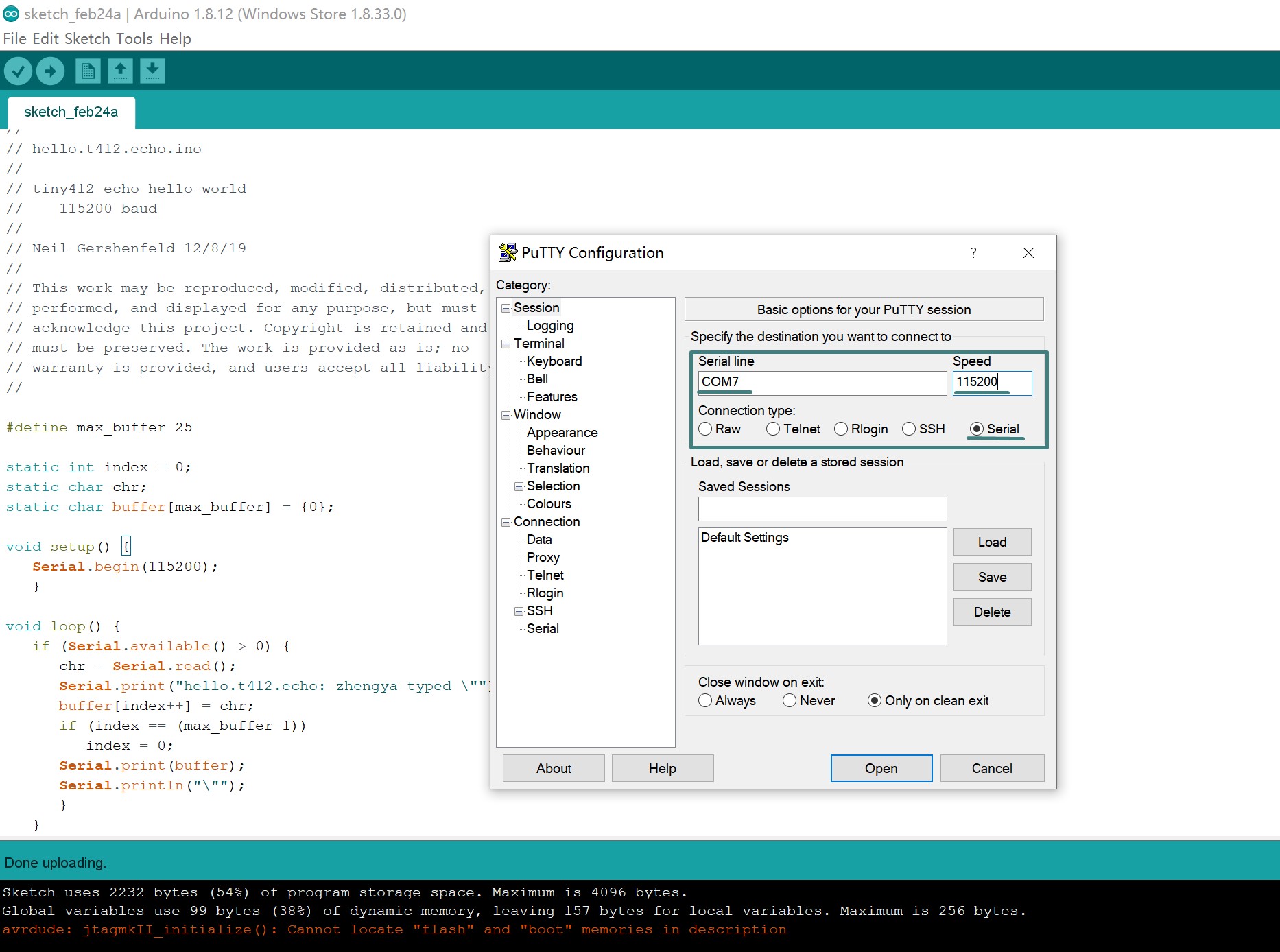
● The PCB need to conenct a USB port for programming. USBtinyISP was used to program the microcontroller with new firmware. The device can be used as a new device in Device Manager.
The Ardiuno Software Tools choose:
Board: “Arduino Nano” Processor: “ATmega328P (Old Bootloader”) Port: COM”the port device connected to” Programmer: “USBtinyISP” Tools> Burn Bootloader
● After that, run a simple program to make the LED blink faster. Now the PCB is an Arduino board based on ATmega328P.
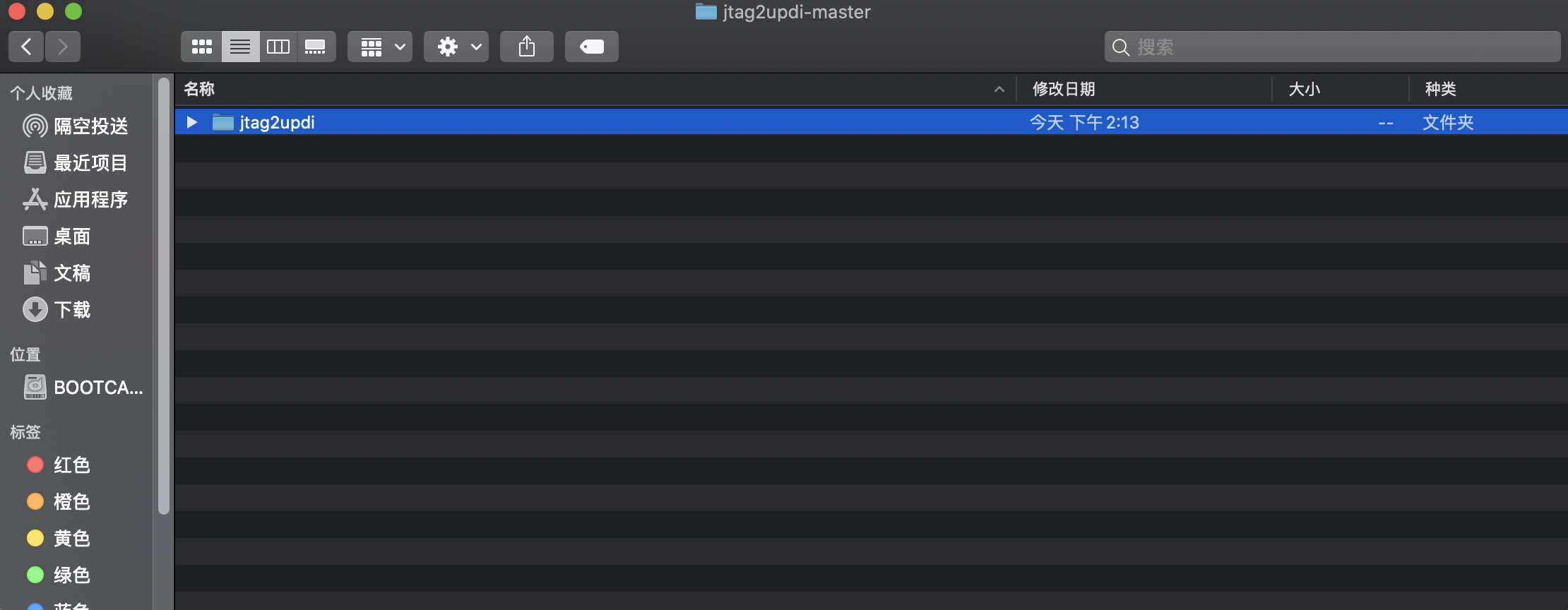
● UPDI programmer can be made by installing ElTangas’s jtag2updi program.
Step1. Downloading jtag2updi and extracting files and created a folder named jtag2updi and pulled other files inside it.
Step2. Opening jtag2updi.ino in Arduino environment that need to be used for compiling, and the code is contained in all the other files.
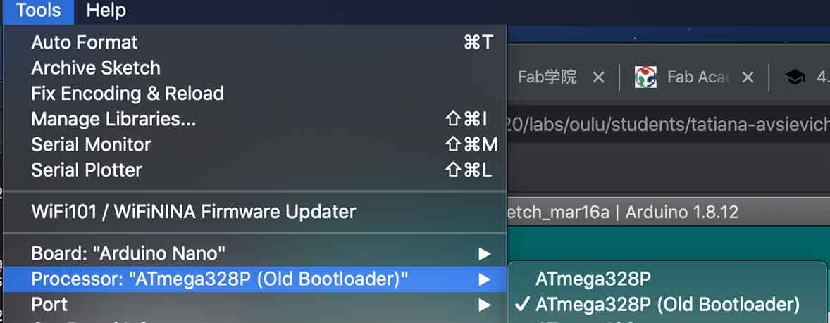
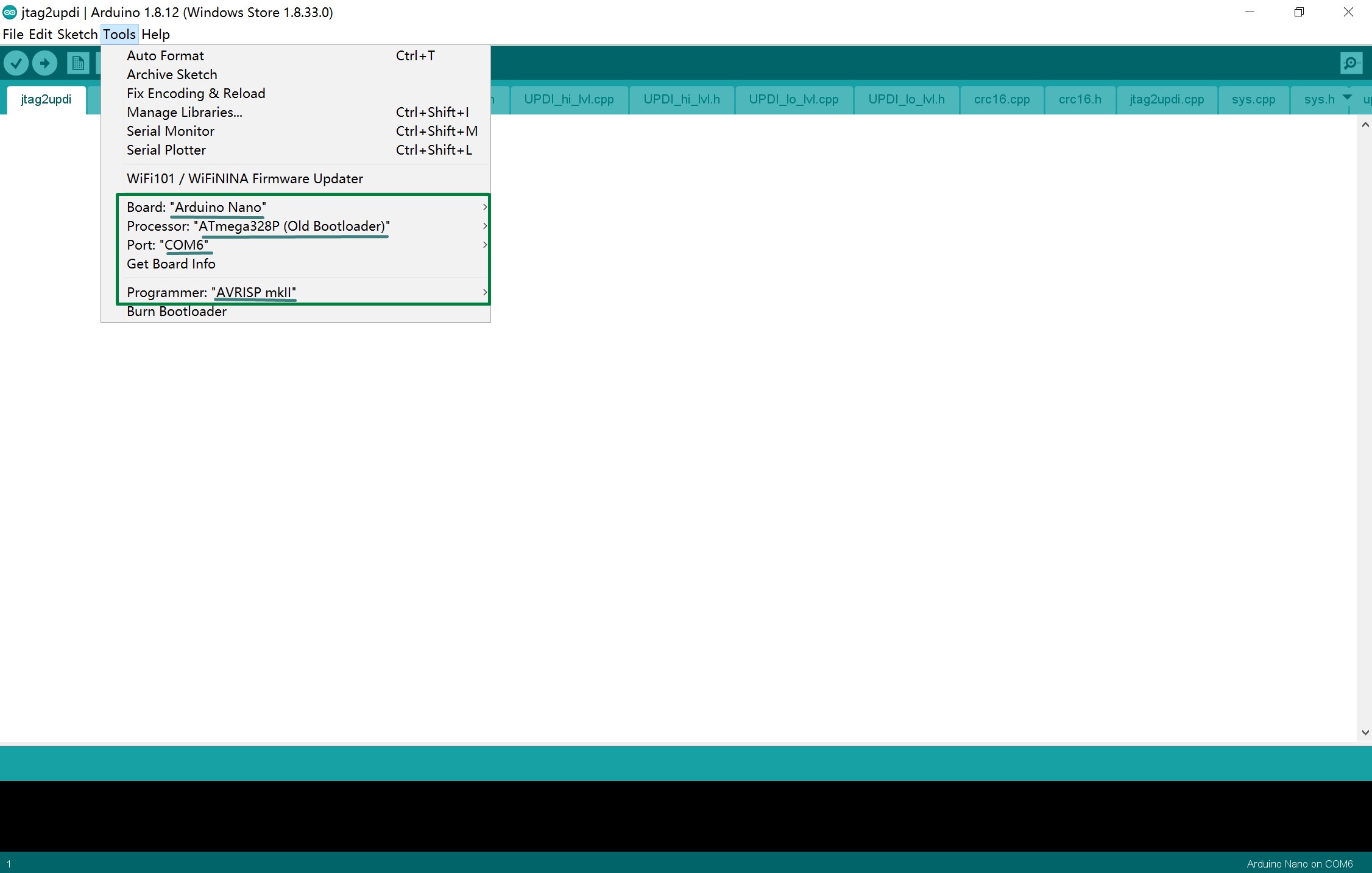
Step3. Setting up the tools.
Tools: Board: “Arduino Nano” Processor: “ATmega328P (Old Bootloader”) Port: COM”the port device connected to” Programmer: “AVRISP mkll”
Step4. Pressing Verify and Upload.
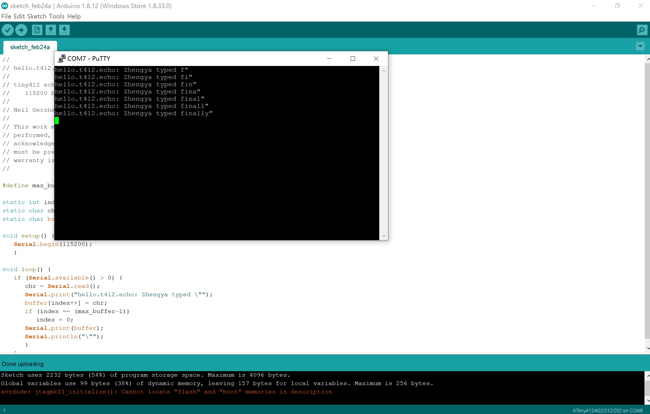
● Programming the ATtiny412
Before programming the ATtiny412, cutting the jumper is necessary, and I cut the jumper that connecting microcontroller and FTDI, and if in the next step, the PCB board is not working, I need check the PCB board or replace the components and soldering the jumper again, and actually, I did the step of soldering the jumper twice, also cutting it 3 times.
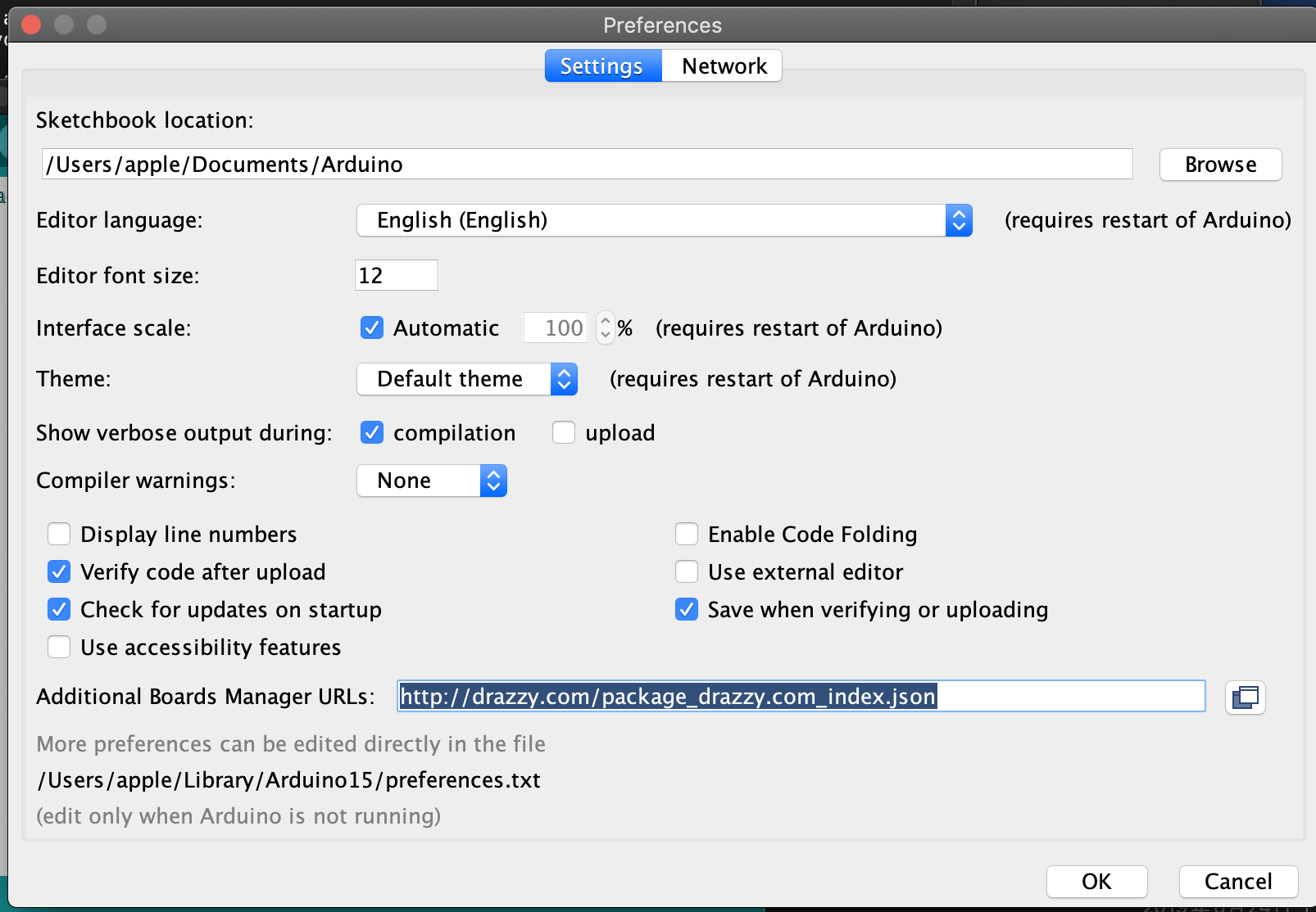
Step1. Installing the megaTinyCore
Go to File > Preferences or Arduino > Preferences, and locate the “Additional Board Manager URLs” text box and enter http://drazzy.com/package_drazzy.com_index.json into the field as shown below and click the OK button.
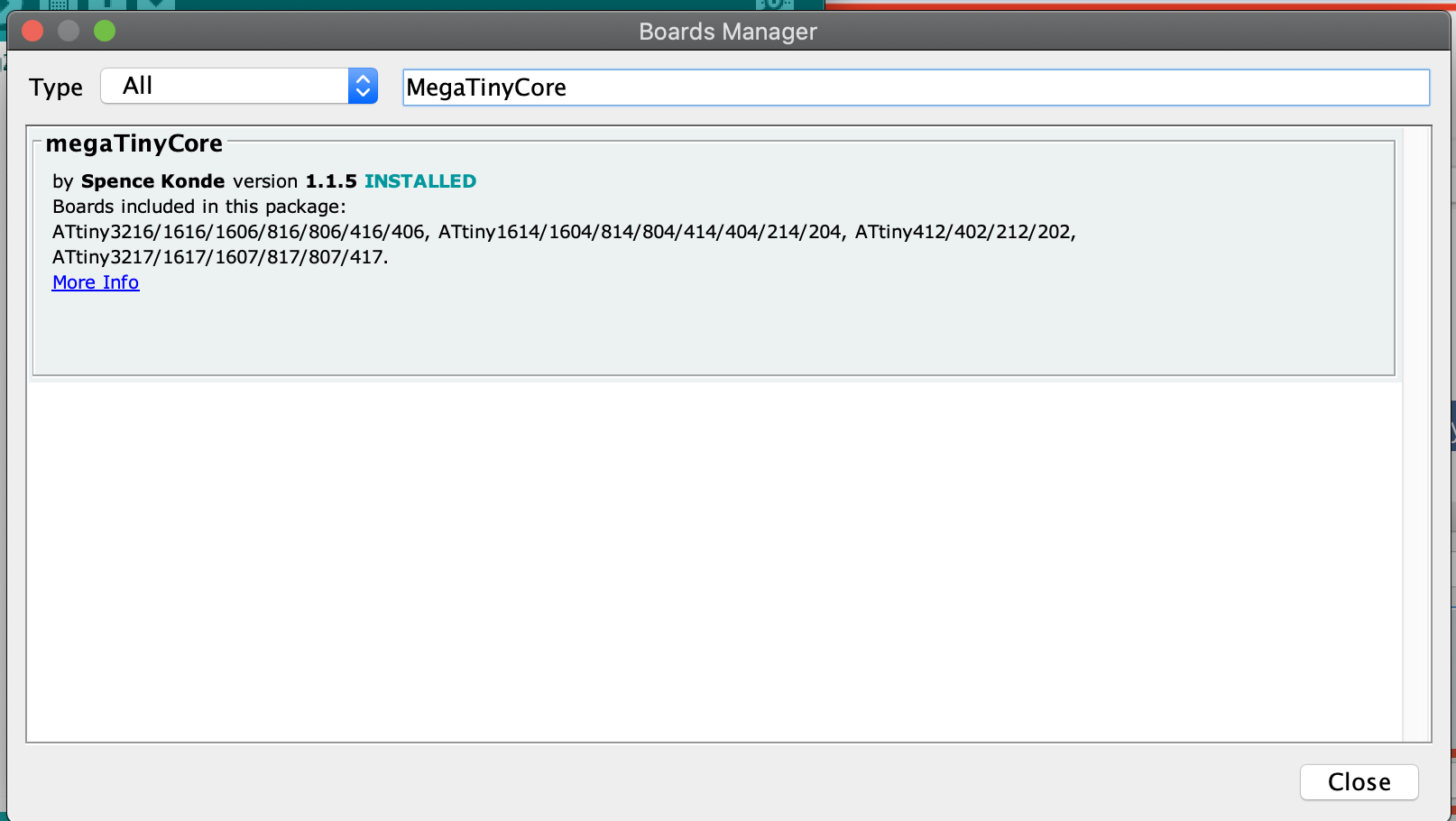
Go to tools>Boards>Boards manager, enter megaTinyCore into the search bar and scroll, click on install.
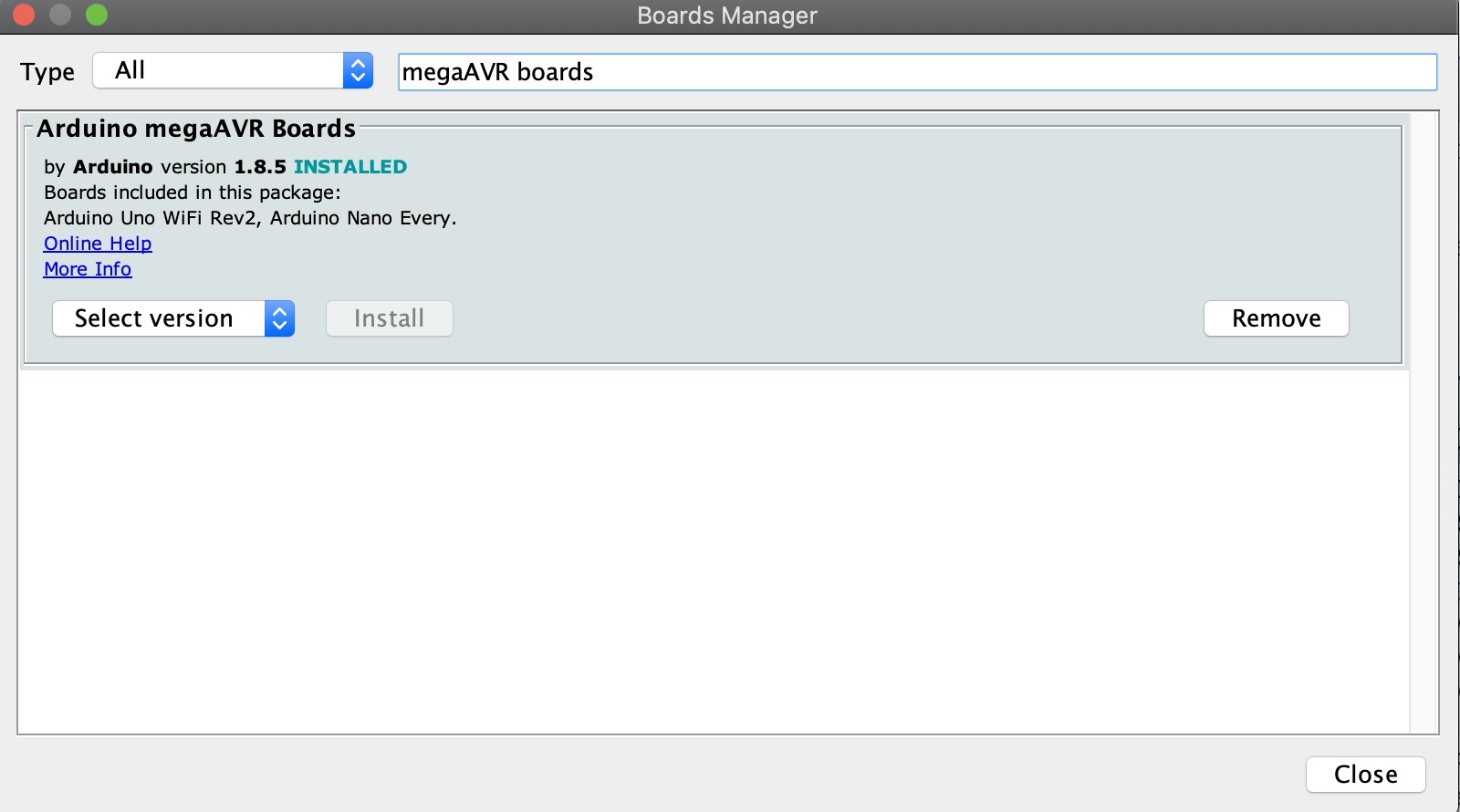
Go to tools>Boards>Boards manager, enter Arduino megaAVR boards into the search bar and scroll, click on install.
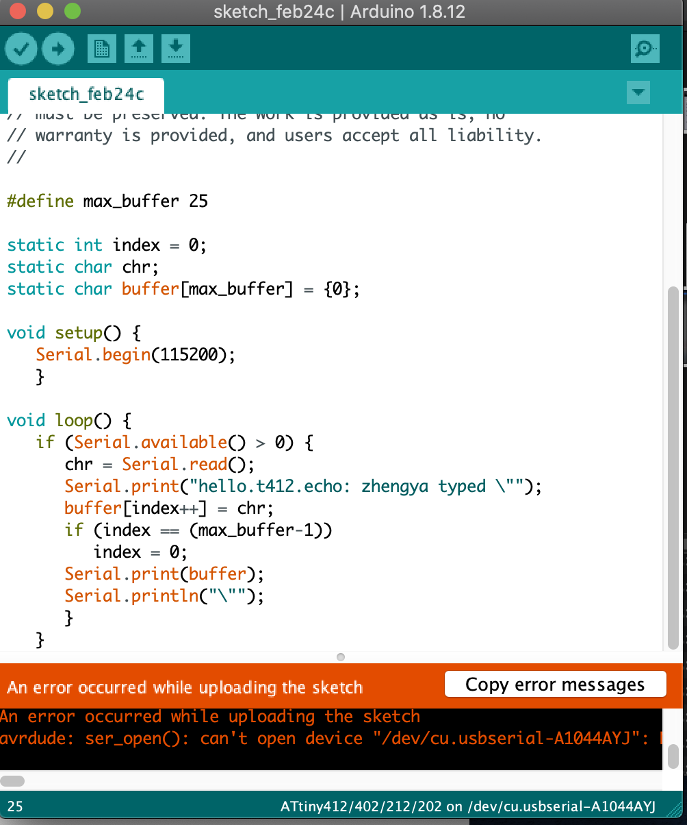
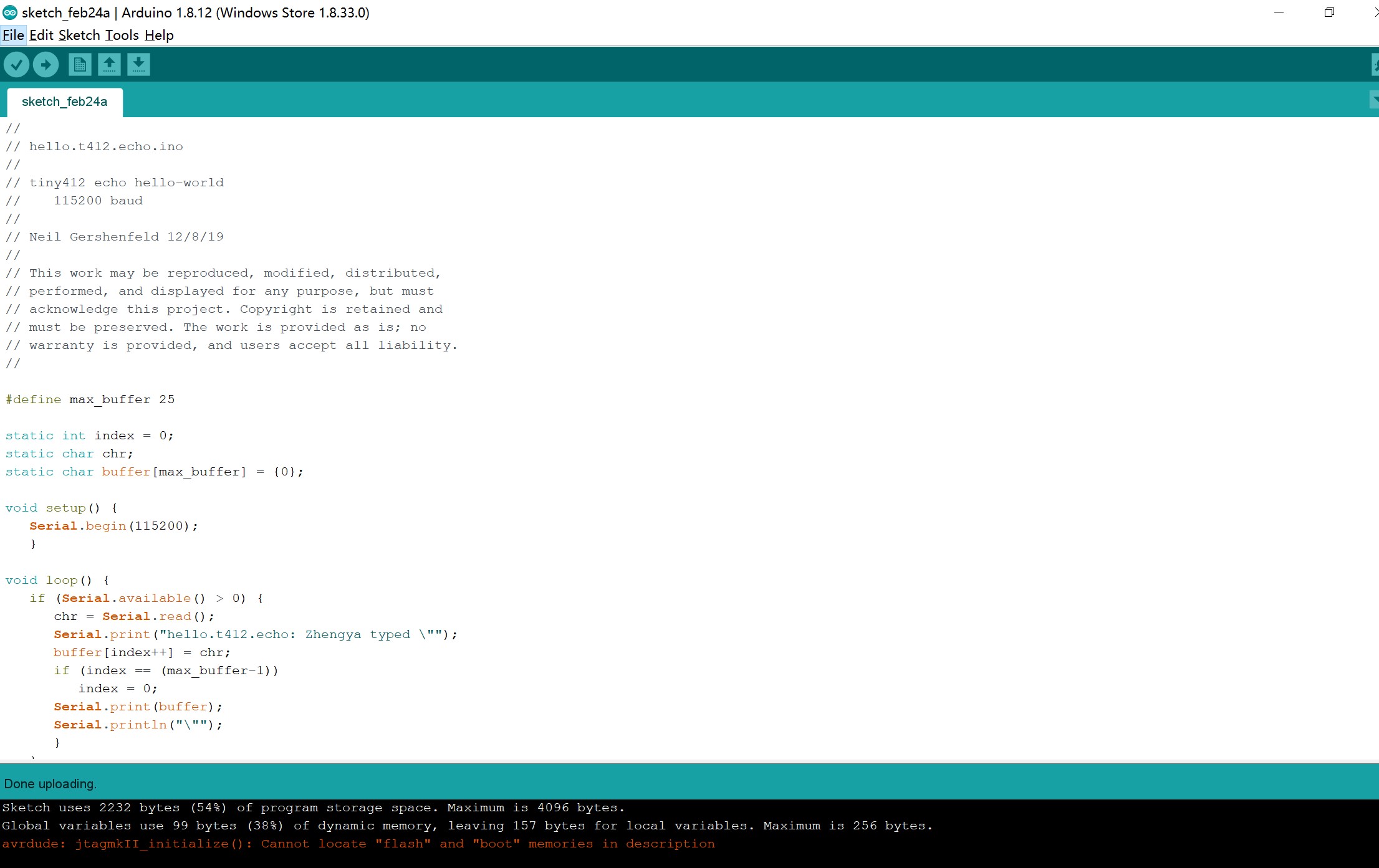
Step2. Connect the board with ATtiny and open a new file and copy the -text as the figure, then upload it.
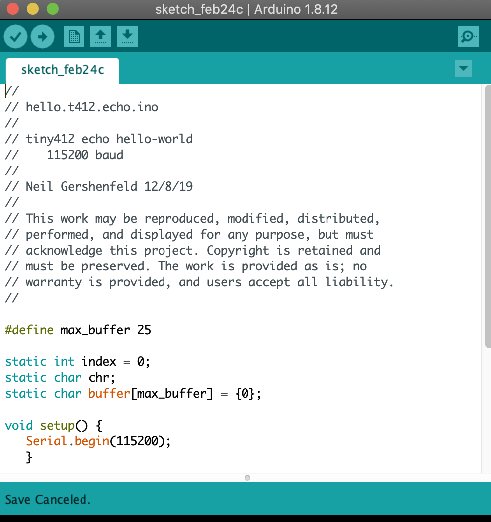
However, in this step, I do not know the reason why my screen showed that. I tried to check it using a microscope and changing the LED, also using laptop of my colleague, and test other’s board using my laptop.
Tuesday, I checked all the connections using a microscope and continuity tester, also replace some components, such as a microcontroller, and soldering it. While, Antti helped me a lot, and he is a professional soldering and very nice. He helped me programming the board again, then I compiling and uploading it using Xinhui’s laptop, she taught me to step by step, and finally, my board is working.
Reflection
For me this week, the challenge was programming, because this is my first time to programming, and I don’t know how to do and how to check everything. However, in the end I seemed to understand the function of each step and completed the work. Maybe I’m not as smart as everyone else, but I work harder although the process makes me crazy。