7. Electronics design
Electronics again… I really need to start from scratch here. So I am following carefully some tutuorials.
Eagle
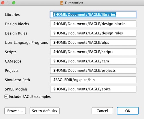
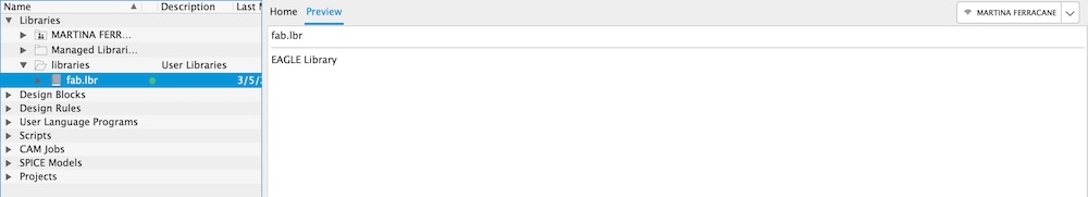
I took this tutorial to start with. First thing I had to do was to import the Fab library to EAGLE. The tutorial made it look simple but the path suggested did not really work with me. First of all, I had to download the entire repository because I did not see any other way to get the library file. Once downloaded, I put it in the folder ‘cache’ > ‘ lbr’. Then I tried to put the library under ‘use’ but again it did not work well. Finally, I found this tutorial and followed it to set up my library.
|
|
Here the main commands to use in EAGLE:
- add = opens up the libraries so that you can add components in Schematic view
- move = moves an item
- net = makes a logical connection
- junction = adds a junction
- value = addes value to components (i.e. ohm rating)
- name = names a component
- label = displays the name of a component in schematic view
- copy = copies an existing component on the schematic.
- route = used in Layout view, this tells you if you need to add a connection (follow yellow lines)
- ERC = electronic rules check; this ensures your board will actually work (use in schematic view)
- DRC = design rules check (in board view) - keep all the default settings (16 mil is fine); it should display a “no error” message in the bottom left hand corner of the screen
- group = groups components in Layout view together; if you right-click, then you can choose Move: Group to move the grouping
- rats = in board view, tells you if you have airwires
- rip = deletes connections in layout
- show = after typing this, select a component to see information about it displayed in the bottom left corner of the screen. Also, if you type show + [name of component] you can see that component highlighted. You can use this to see all the ground traces, for example.
- text = allows you to add text to your board. You can also edit the exported .png file in The Gimp to give text and black and white line images. I recommend adding text in The Gimp.)
- info = then click on text to get properties of the text
Add components to the schematic view
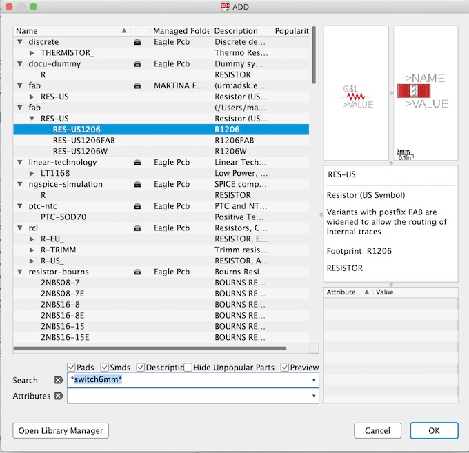
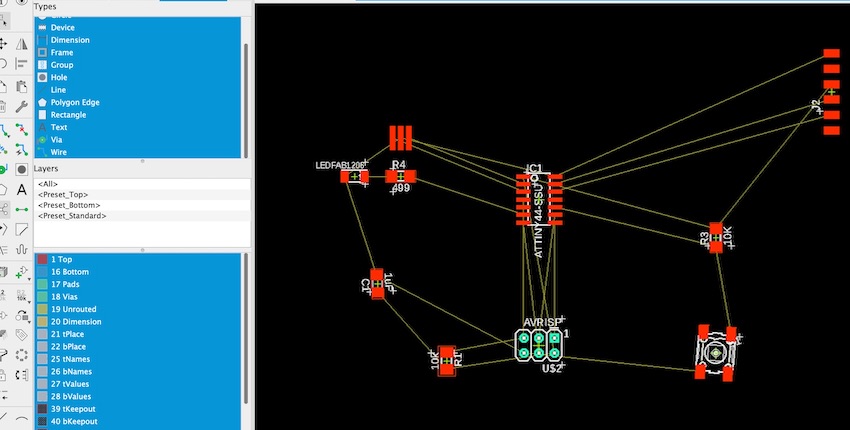
Adding the components is quite simple. Just use the command ‘add’ and select the components needed. It is possible to put the word in between asterisks.
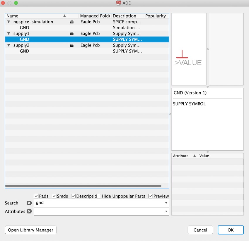
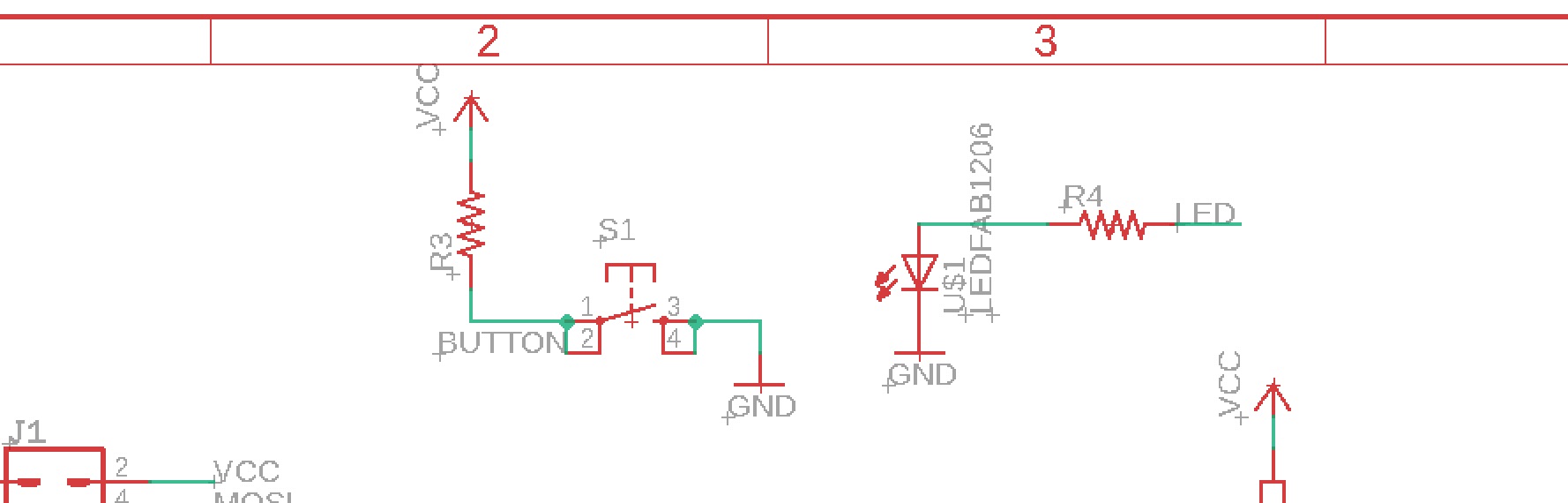
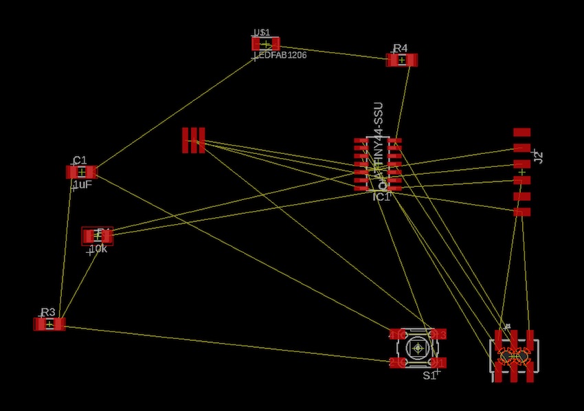
I got all the components to the schematic. The only doubt I have is about the GROUND. By searching ‘ground’ I only get one option. But in the schematic there is another sign for the ground. I’ll use the one in the schematic, but I’ll check if there is any difference.
|

|
But at this point I was stuck as in the tutorial it didn’t say how they were supposed to be connected. I gave it a try by following the image and I hope it all is correct.
Verify the design using the ERC (Electrical Rules Check)
The tutorial only mentioned ERC without going into details. I used it and found no errors, but a few warnings.
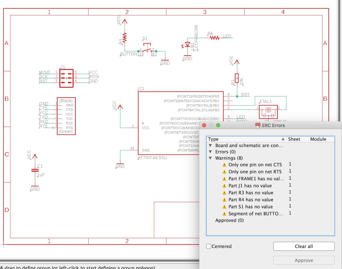
For most of them, I did not really understand what they were about. It seems that values are missing from resistors, which makes sense. I will try to address this once I am done. And also there was a missing label for pin 10, which I have added.
Board view and place the components and route the traces
Once this was done, I switched to the board view.
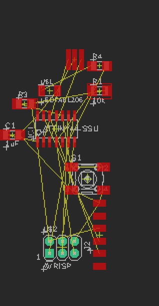
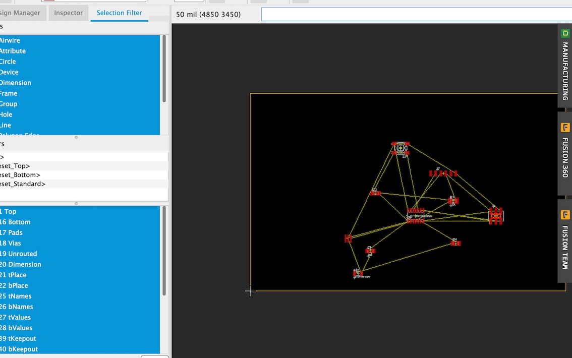
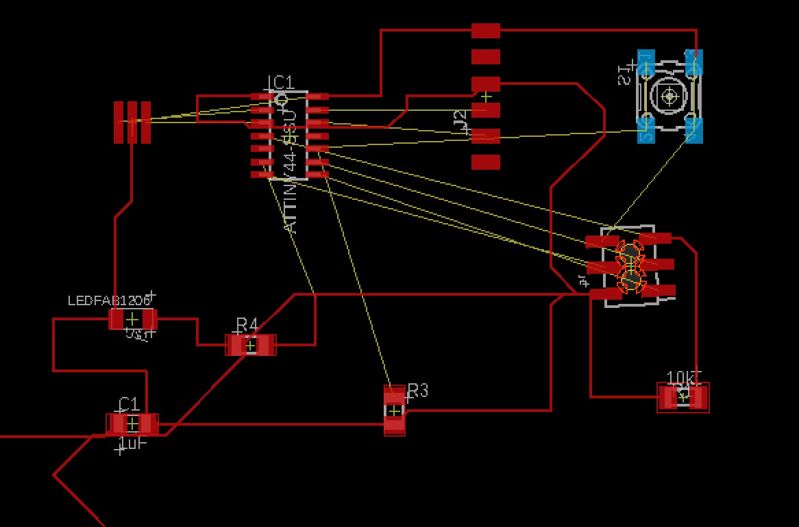
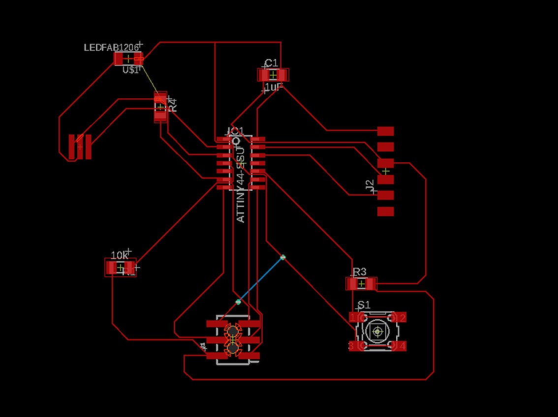
And this is where the trouble began! I tried without success to create the board and I always failed to make it a way that lines did not cross each other. I tried the autorouter but it seems it keeps the position of the components, so it did not make a good job and created one blue connection (which I learnt is a trace on the bottom layer which I would not be able to mill!).
|
|
|
|
|
|
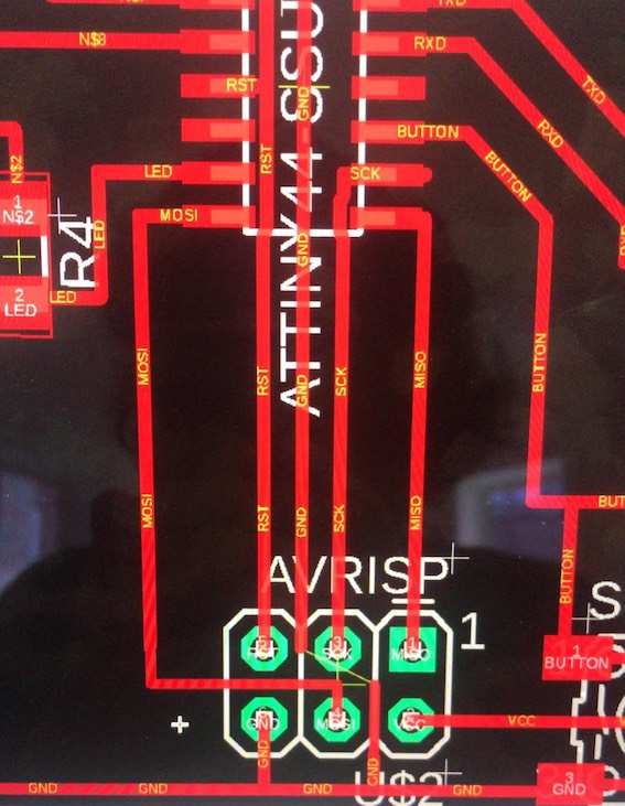
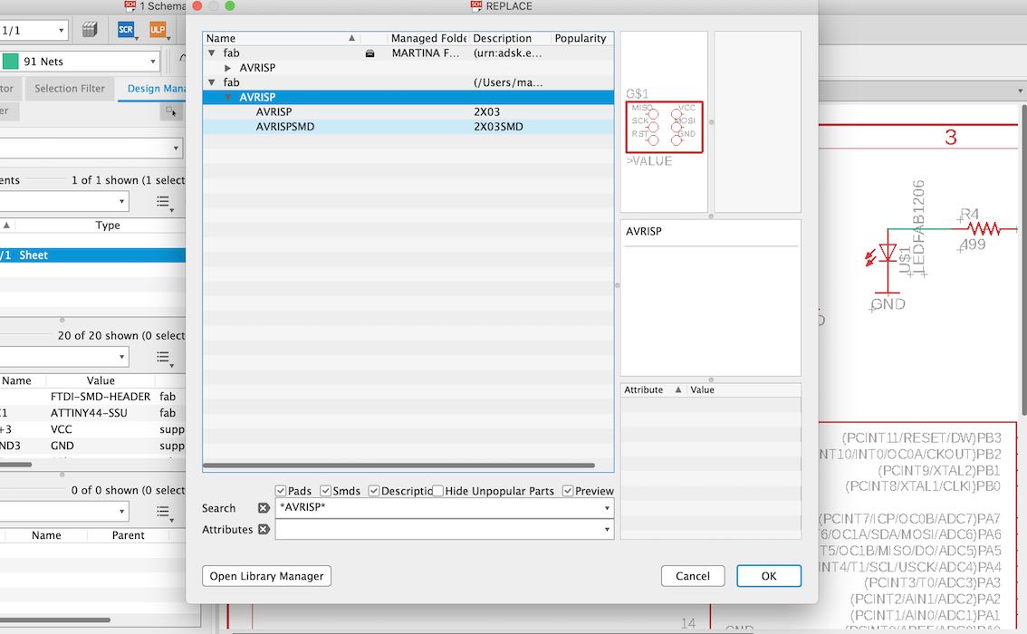
I asked thought the problem could be solved by switching the component with another component under which I could make traces, so I asked the tutor for an alternative component and he suggested the AVRISP 6 pins hearder. So I changed the component and named all pins. But it did not help much with the current design…
|
|
|
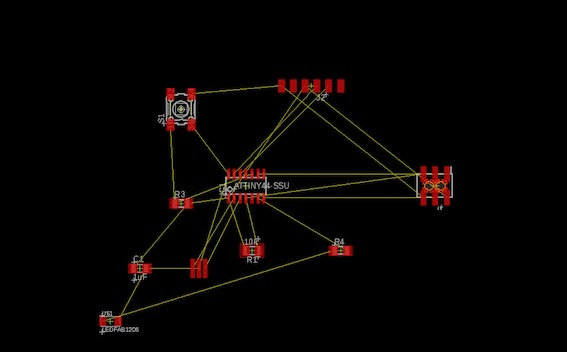
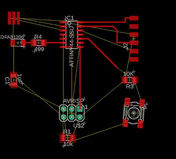
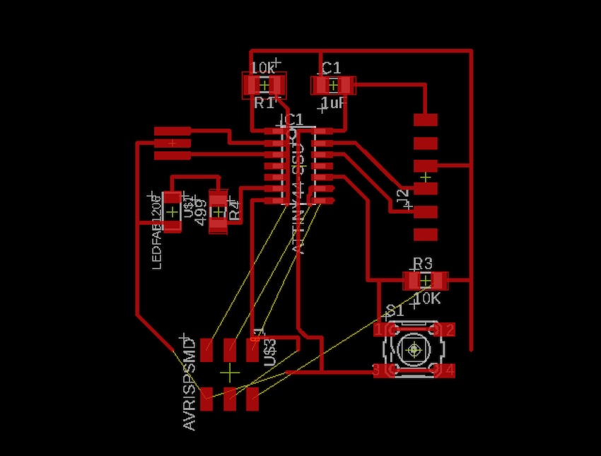
So I started again from scratch and this time followed this image which was in the tutorial!
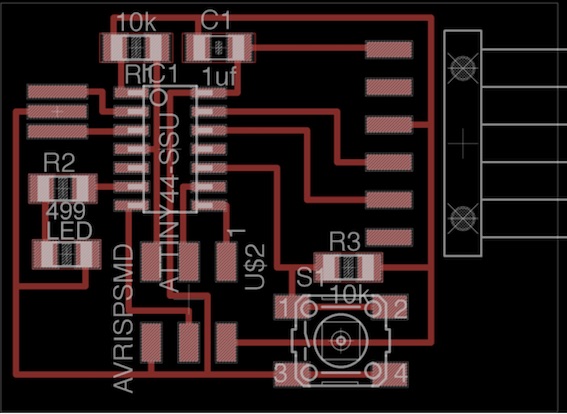
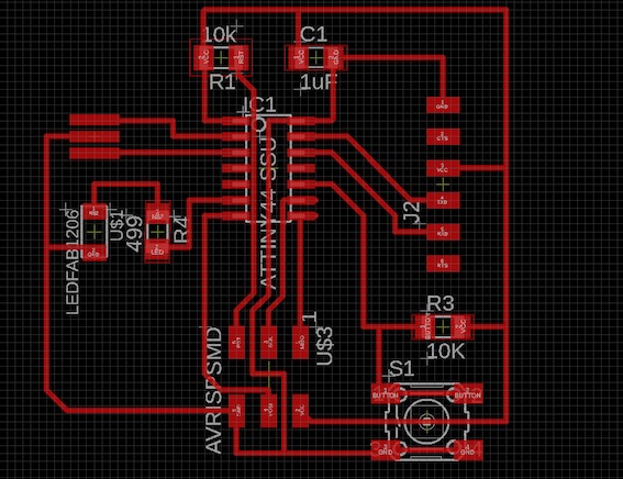
I managed to finalise the board but I did not have much space between the lines.
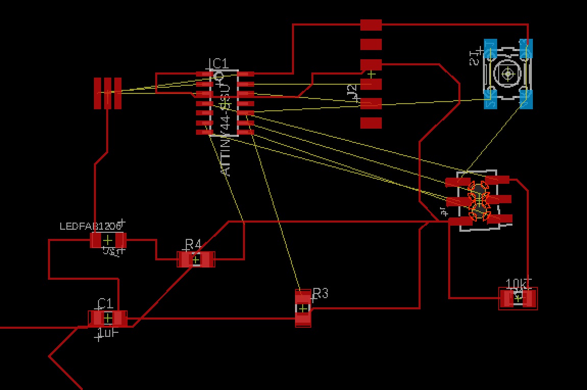
My tutor told me I had chosed the wrong component 2*3 and I was better using one that had more space for the traces. So I changed the component.
|
|
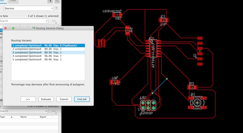
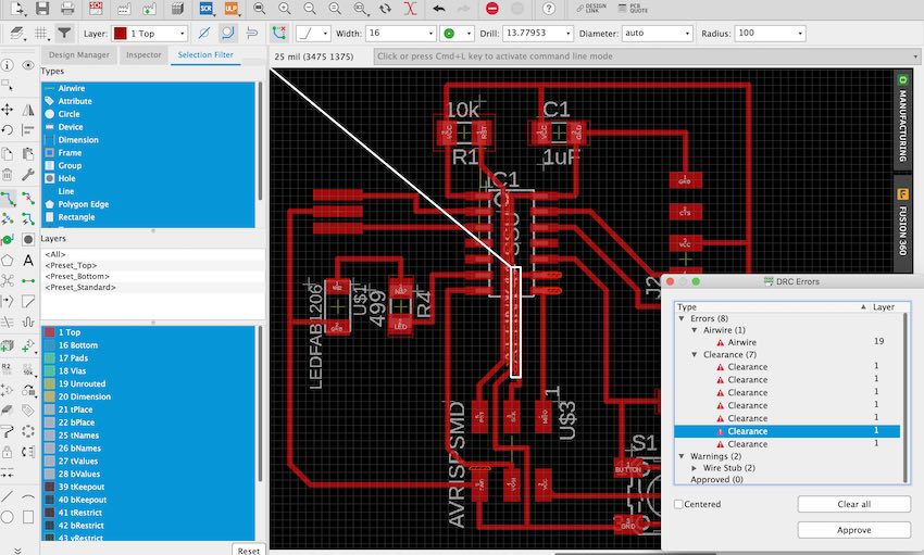
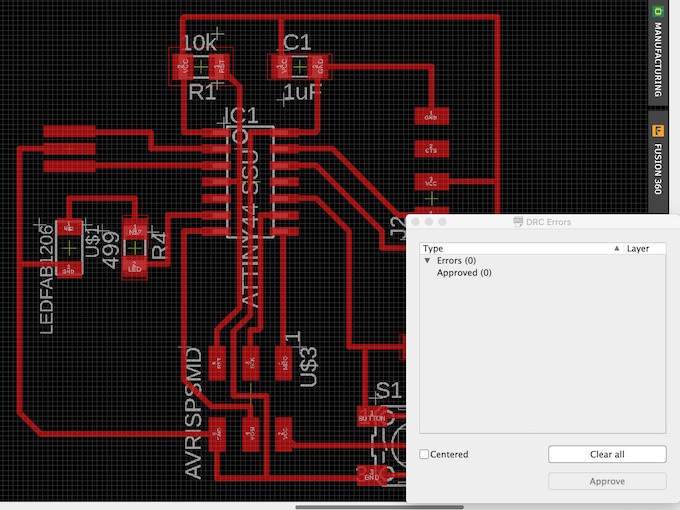
Verify the design using the Design Rule Cheking (DRC)
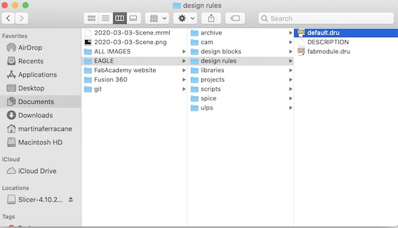
I had to verify now the design rule cheking (DRC). I donwloaded the fablab file for DRC and added it to the folder of design rules.
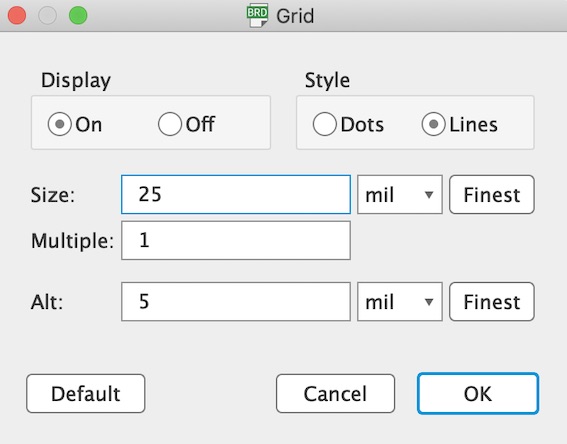
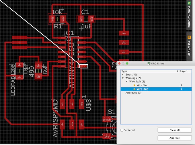
The verification found a few issues. The main one was that the traces were too close to each other. I changed the size of the grid and this was enough to move the lines slightly, so that they would all fit and be separated one another.
|
|
|
|
And after that the board was finally ready to be exported!
Exporting the board design
I first have to select only the top layer view.
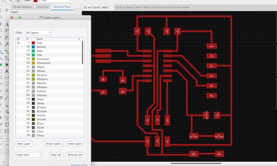
Then selected ‘monochrome’ and a DPI of at least 500 dpi (1000 dpi would be even better), and also window in order to avoid having too much empty space.
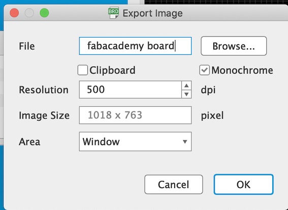
Then the board was ready to be exported. However, with Mac, there is as size error for export. So I instead used a Linux computer to export the image.
Here my Eagle files.
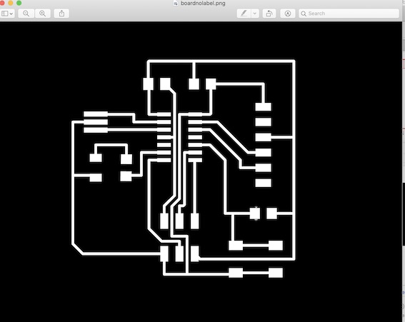
Create traces & interior with GIMP
I used GIMP to finalise the design of the board traces and interior. First thing was to crop the image, then add 20mm width and center.
I then tried to create the interior with a brush, but since I did not know well how GIMP worked, the result was not very good. I tried anyway to mill and see if it worked.
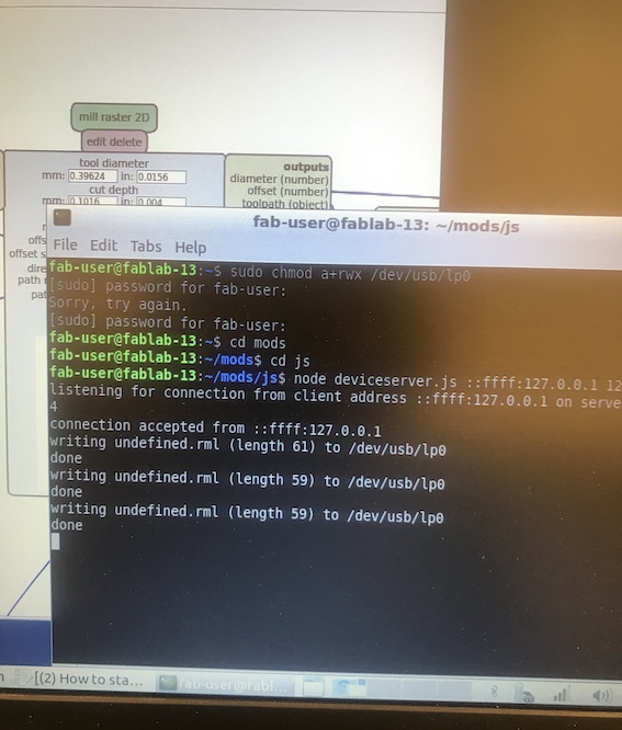
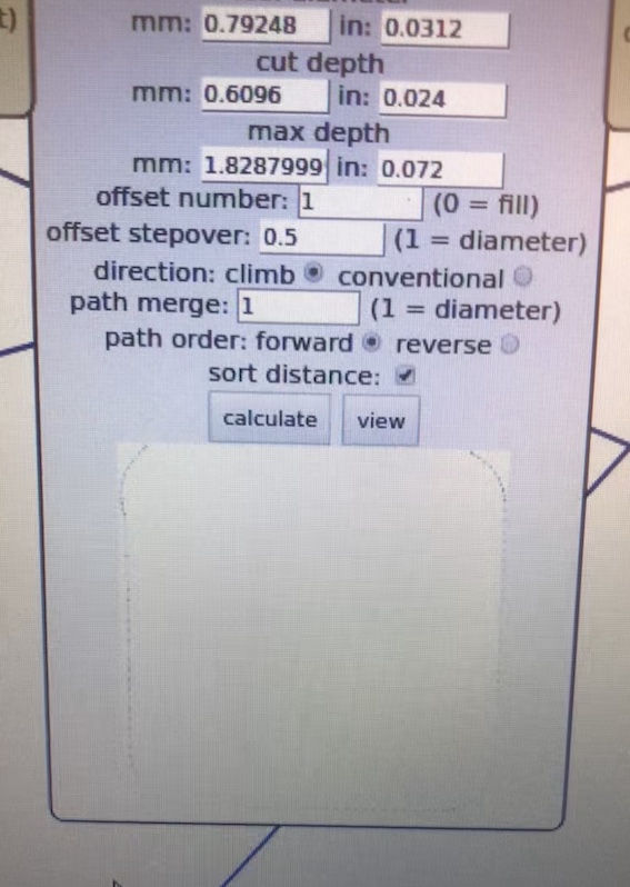
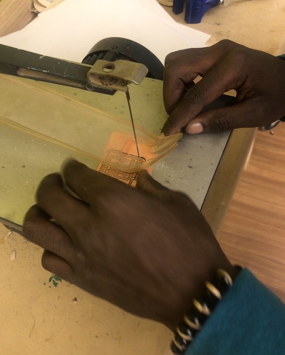
Milling
I did this part of the week at Lena Park. I had never used the milling, so it took me some time before I managed to operate mods.
The traces went fine, but I had a problem with the interior.
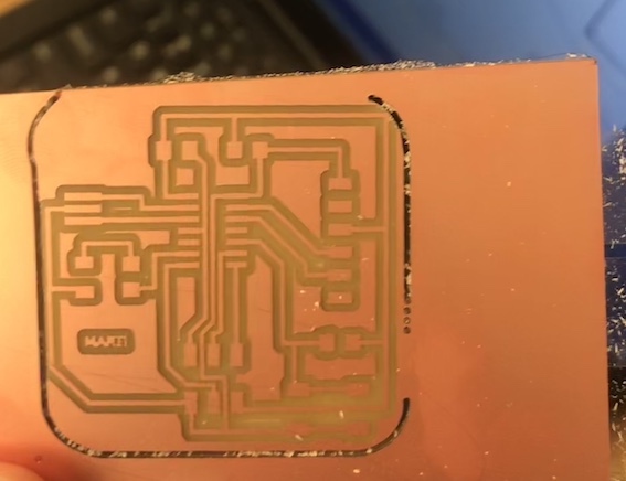
The line for some reason was not correct, so it did not cut all the way through. I got some help in the fablab to manually cut the parts which went wrong.
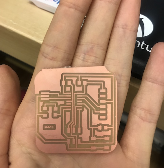
And here the final result:
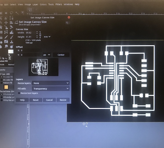
Later on, I went through GIMP again with my instructor and learnt better how to prepare the image for milling with GIMP.
 First I need to resize because there is a bug for mac and I learnt how to do with GIMP. I click on image, then scale image and then set it to 50%.
 Second, I learnt how to crop: I have to select the crop tool on the tool bar on the left and then click once inside the image to finalise the crop.
 Then on the right side, I can create a new layer. In this layer, I can use the pencil tool to create the interior
Here my images created with inkascape which were not a good resolution and did not work.
Here my final images which worked well.
In the future, I want to test creating the exterior and interior directly with EAGLE as this student did.
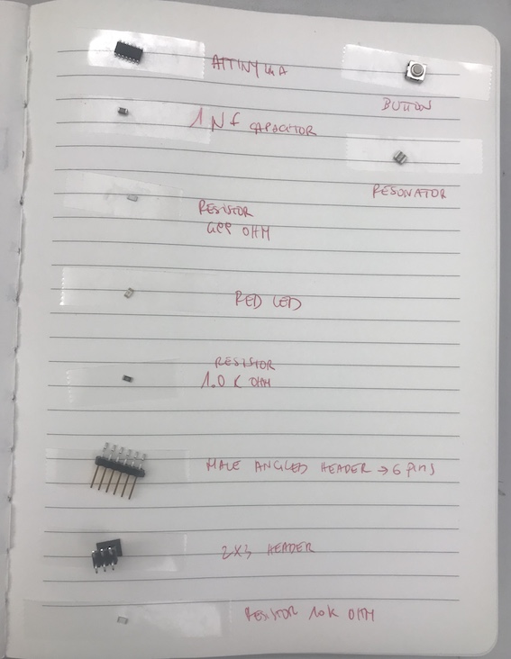
Soldering
Finding the components was not straightforward.. I asked the help of the tutor to find some of them.
Testing
To test the board, I used a multimeter. Luciano gave us a class about the multimeter which was very detailed!
First I checked the continuity
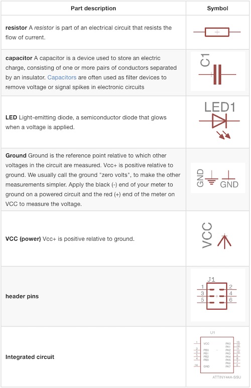
Terminology
- CURRENT is the directed flow of charge through a conductor.
- VOLTAGE is the force that generates the current.
- RESISTANCE is an opposition to current that is provided by a material, component, or circuit.
- Board layout shows how the - electrical components and traces will be laid out on the board.
Fun of the week
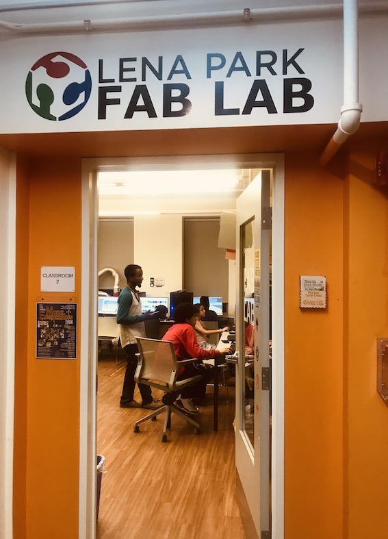
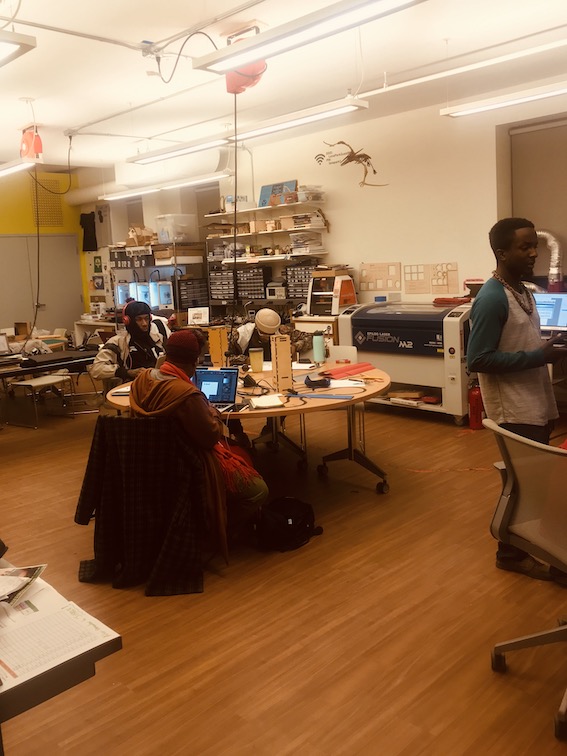
This week I discovered the Lena Park FabLab in the Lena Park Community Center.
|
|