7. Electronics design
This week’s tasks:
Group Assignment
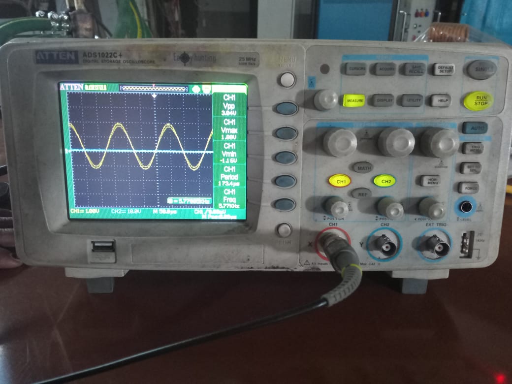
- Use an oscilloscope and try out its various functions.
- Learn about the Safety features and how to properly ground the Oscilloscope.
Individual Assignment:
- Experiment with EDA softwares
- Design a helloworld board.
- Program the board.
EDA Softwares
I explored two softwares one is KiCad and the other is Eagle. These two are the best.
KiCad
KiCad is an EDA software which is very powerful and is open source and best of all its free!. I explored the software for a bit and I have installed a few libraries by following tutorials. The libraries installed were Sparkfun and fab, the libraries contain component footprint, schematic symbols, pin definitions and a bunch of other stuff. Most big component retailers make and catalogue these libraries for the convenience of the user but we can create a library of our own. Although I have not explored that part of the software, I intend to do so in the future.
Eagle
Eagle is an EDA software that was initially created by CadSoft which was bought by Autodesk in the year 2016 and having a little experience in using it during my college days I chose it as my go-to software the ease of use was a bonus. I added the Fab, Adafruit and Sparkfun libraries and the process was fast. The advantage of using Eagle is that we can render a PCB and export it to Fusion by doing so we can create enclosures and other housing by being a bit creative.
Designing PCB
When we design a PCB be it in Eagle or KiCad There will be two files created one is Schematic file other is board file, Schematic file is where we create a circuit as a reference for the board file, in the schematic file we assign values to each component such as a resistor, capacitor, diode, oscillator, etc. Schematic file To begin with, click on the icon ‘Add Part’, upon clicking it we will get the list of libraries to choose the appropriate library, select the component and click OK. The components once added, connect them to make circuit clicking on the NET icon on the toolbar.
One thing to be careful about is, see that all the nets are connected otherwise we can expect errors while designing the board file
You can avoid this by using ERC tool which will help you in detecting errors
Board file
This step is a tricky part in designing a PCB; we have a lot of factors where we must exert caution. During this process, there are a few tools to take note they are:
- DRC
- ERC
- Rats nest
- Auto route
- Meander/Rip up
DRC
DRC stands for Design Rule Check. First We need to set up a few things such as the thickness of our traces the size of our pads, the drill diameter, etc. In DRC set the clearances as you desire my comfort zone for clearance is in between 12-16 mil and for trace thickness, it is in between 8-16 mil.
RATS NEST Rats nest is a tool which can be like double edged sword from my experience it can either simplify your design or complicate your design be very careful while using it.
ROUTING
There are two ways to route in eagle, manual and auto routing. Manual Routing is a simple process where we are just connecting two points this serves two purposes if you want to get creative and add a personalized touch we can do so using manual routing also we can correct errors or open nets using this option.
Auto Routing is a tool which automatically connects the nets, using this tool we set can preset the number of layers on which the nets could be drawn, by which we can significantly cut down designing time. The only downside is that sometimes the placement or the way components are connected; the tool can have a hard time connecting components; this is observed in single-layer boards.
eg:
AUTO ! GND VCC;
RIP UP
Rip up is a tool used to remove nets that have been placed in between a pad or device
SYNTAX
RIPUP;
RIPUP [ @ ] [ ! ] •..
RIPUP [ @ ] [ ! ] signal_name.
Additional Tasks
- Simulate a Circuit.
Gallery
Video
Intro to Oscilloscope:
The videos below help viewers understandhow to use
How NOT To Blow Up Your Oscilloscope: