6. Electronics design
individual project
i have to redraw ATSAMD11C hello.D11C.echo
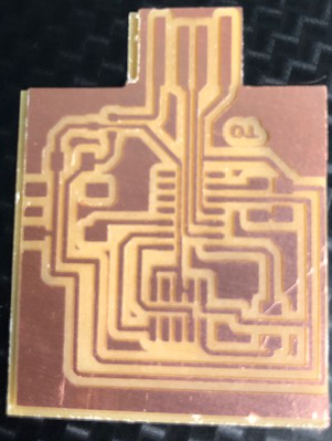
the original design is here : traces
the original component are :
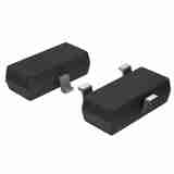
- 1 micro-controller SAMD11C (named IC1D11)
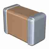
- 1 capacitor 1μF (named C1μF )
- 1 resistor 0 ohm (named R10) as a bridge to avoid a problem of design
- 1 connectors 10 pins (named J1SWD)
- 1 integrated circuit 3,3 v (tension regulator named IC2 3.3 v)
all the component selected by the fabacademy are here
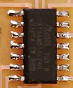
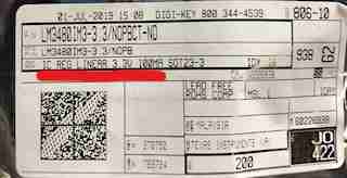
we need to determine the mounting direction of this component. it’s possible by comparing the documentation and the picture.
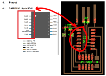
tension regulator LM3480IM3-3.3/NOPB

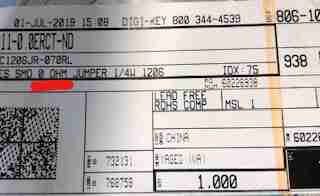
connection header 10 pins 20021121-00010T1LF and the technical sheet page 8
in this case, to find to footprint, you can use https://app.ultralibrarian.com/search?queryText=20021121-00010T1LF and also https://gitlab.fabcloud.org/pub/libraries/electronics/tree/master/kicad to update kicad with the components selected by the fabacademy.
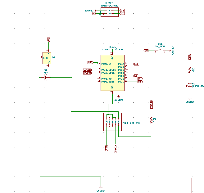
added component :
and the LED need a resistor as protection (current-limiting)
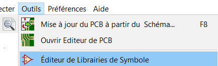
i draw with kicad.
i have to import a library components from the fabacademy components library to download. the names of the component of the library begin by fab
in the hello.D11C.echo file, i found some information to choose the component in the FAB library
pad_1206 = cube(-.032,.032,-.034,.034,0,0)
class R_1206
1206 resistor
1206 capacitor
Class USB_A_plug(part):
the component in the library are
RES-US 1206FAB
CAP-US 1206FAB
LM3480-3.3
ATMASD11C14A-SS
there is the problem of the 10 pins connector footprint and the USB male connector design. The footprint of the 10 pins connector can be found here. i found this information after designing the PCB, so i’ll explain how i did and not how to add this specific footprint in Kicad.
how to import downloaded files from Ultra Librarian into KiCAD software
one file .lib and one folder .pretty with a .mod inside describe at least the component.
To keep even it after the project i copied those downloaded files .lib in c:\Program Files\KiCad\share\kicad\library, which is named in the kicad configuration ${KICAD_SYMBOL_DIR} and the folder .pretty in c:\Program Files\KiCad\share\kicad\modules which is named ${KISYSMOD}
In kicad, first you draw a eeschema  , with all the components, then
  you generate the netlist file (tools/netlist). After that, you can begin to design the pcb.
Because the male USB in not a components and only a design on copper, i decided to add a 4pins (PINHD-2X2-SMD) connector to simulate it.
i linked the button and the led to free and unamed pins of the ATMASD11. (and ground on the other side)
eeschema is the logical design of the PBC,
maybe you’ll have to add components library to find the correct component like the fabacademy library.
you choose the component 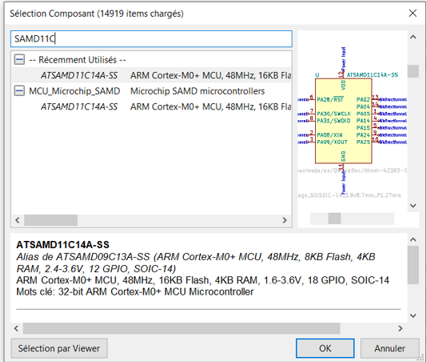 , you place it and you configure it (name, footprint, etc…)and eventualy redefine manually in the right library
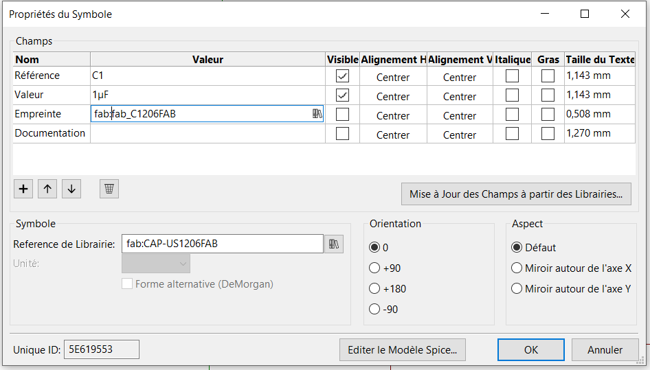 .
.
You draw the lines  between the pins of the different components
 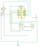 . Check the names of the pines on the component to ensure the links between the different components. To simplify the reading of the design, i use Labels
  .
.
 .
.
When the logical design is finished, the netliste is prepared 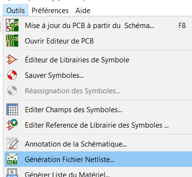 .
.
is used to draw the pcb. import the netliste file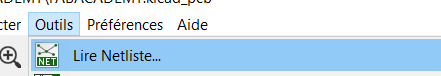 .
.
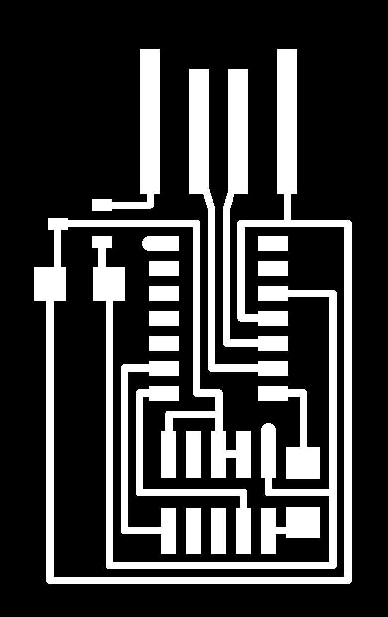
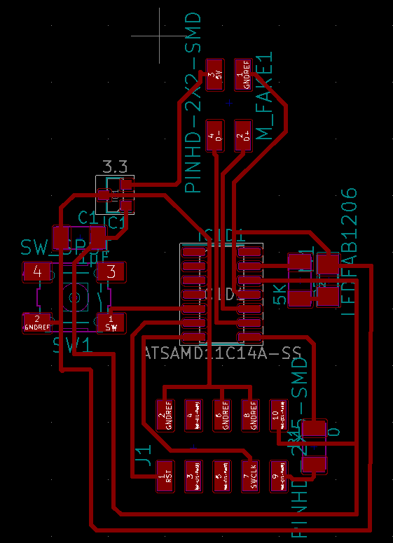
This is the physical design of the pcb. 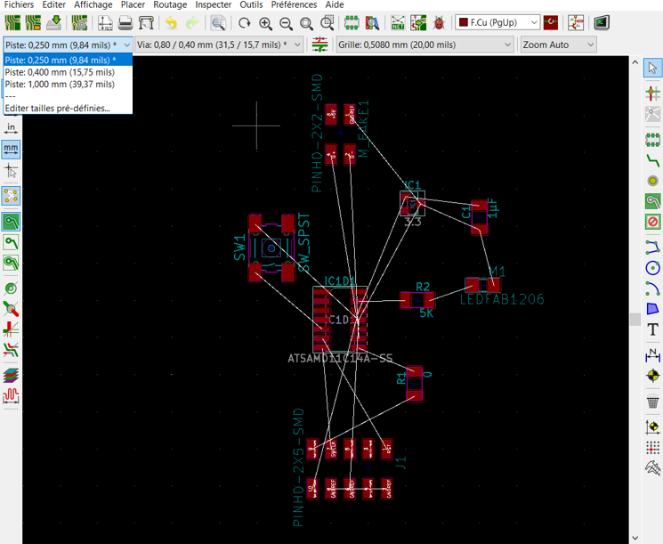 . You have to move, rotate (R) the elements and drawing the lines to replace the white lines.
At this step, i checked that all the original pins of the different components in the original design were respected.
 .
.
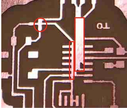
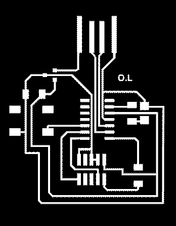
When you use mods, check the view after choosing calculate. you’ll see if all the lines are drawed. When i did it, i noticed that some lines were to wide so redesign those in 0,25. Even with that, the result of the calculation was not good for the traces of the ATMASD11C which was not separate from the closest lines.
i changed directly in the .pnb to fix it and it worked in mods.
if you don’t check the design after calculation on Mods, you can have this type of mistakes.
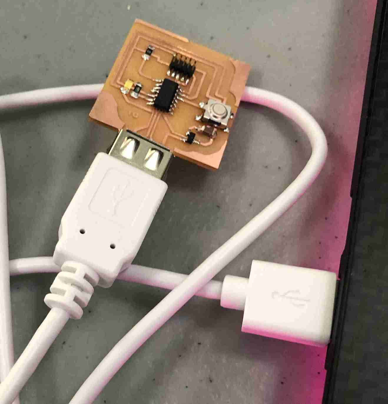
the design of the USB connector
when you want to prepare the gcode for the milling machine, you have to prepare 2 bipmap pictures.
Kicad export in .svg, inskspace (for example) import the .svg and save in .png with 1000 ppp resolution settings and then you have your png file for mods (invert the colors before mods).
At this step, you can copy a part of another design where is the male usb footprint and past it on your design at good place. you make the same with the interior design.
And you can make the same to modify the lines, the places of the component, or if you don’t find the good footprint for a component but you know another design where you can find it.
I did all the final changes with corelphotopaint in the .png file
Final result
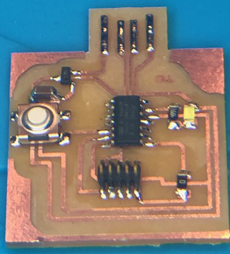
Physical test
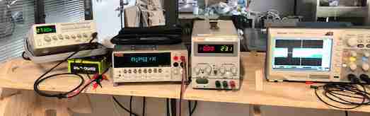
I tested the continuity and the voltage of the designed pcb plugged from the 5V pin to the ground and from the IC to the ATMASD11C14A-SS for 3,3 v
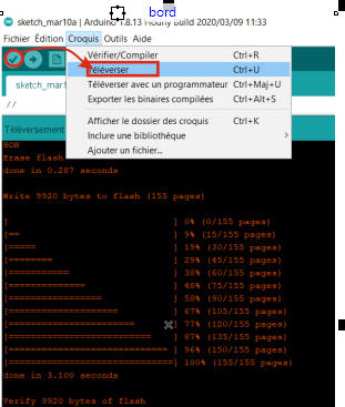
Flashing
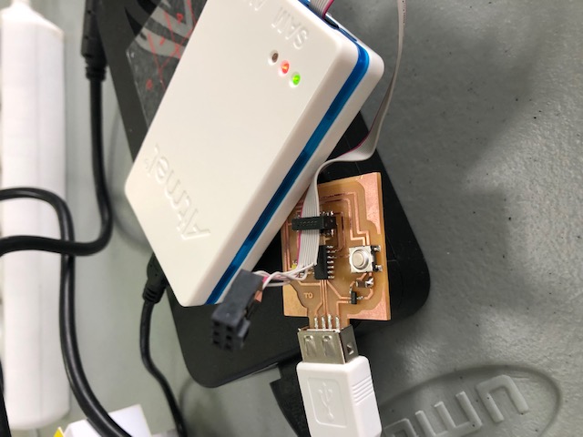
first download EDBG and Generic_D11C14A_SAMD11C14A.bin in the same folder
rename the edbg-b74-WINDOWS-7029fc4.exe in edbg.exe
in a CMD windows, in the right folder, type
edbg -b -t samd11 -pv -f sam_ba_Generic_D11C14A_SAMD11C14A.bin
it will install the bootloader in the pcb so the computer will recognize it when you plug it un his USB port (specific sound)
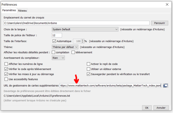
you need to install Arduino to flash the pcb. then, you need to add information, step by step.
https://www.mattairtech.com/software/arduino/beta/package_MattairTech_index.json
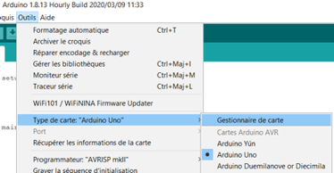
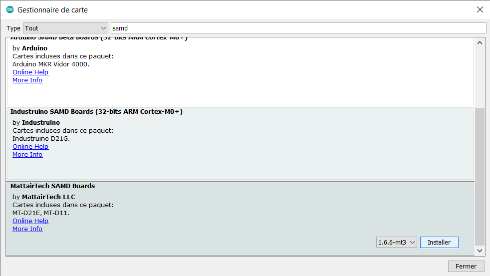
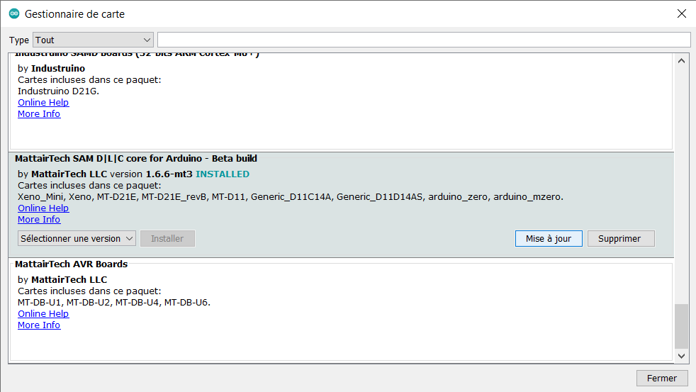
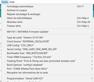
with Adruino, in tools, type of card, choose D11C14A
Copy the text echo.ino in arduino
finally, the correct configuration in arduino is like that
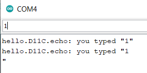
the final test
After copying the text of the echo.ino
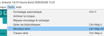
then you use the terminal mode to type a text and the pcb answer the same text.
group project:
use the test equipment in your lab to observe the operation of a microcontroller circuit board