7. Electronics design
Group assignment: Use the test equipment in your lab to observe the operation of a microcontroller circuit board.
Individual assignment: Redraw the echo hello-world board, add (at least) a button and LED (with a current-limiting resistor), check the design rules, make it, test it.
Extra credit: Simulate its operation. Render it.
Using the equipment
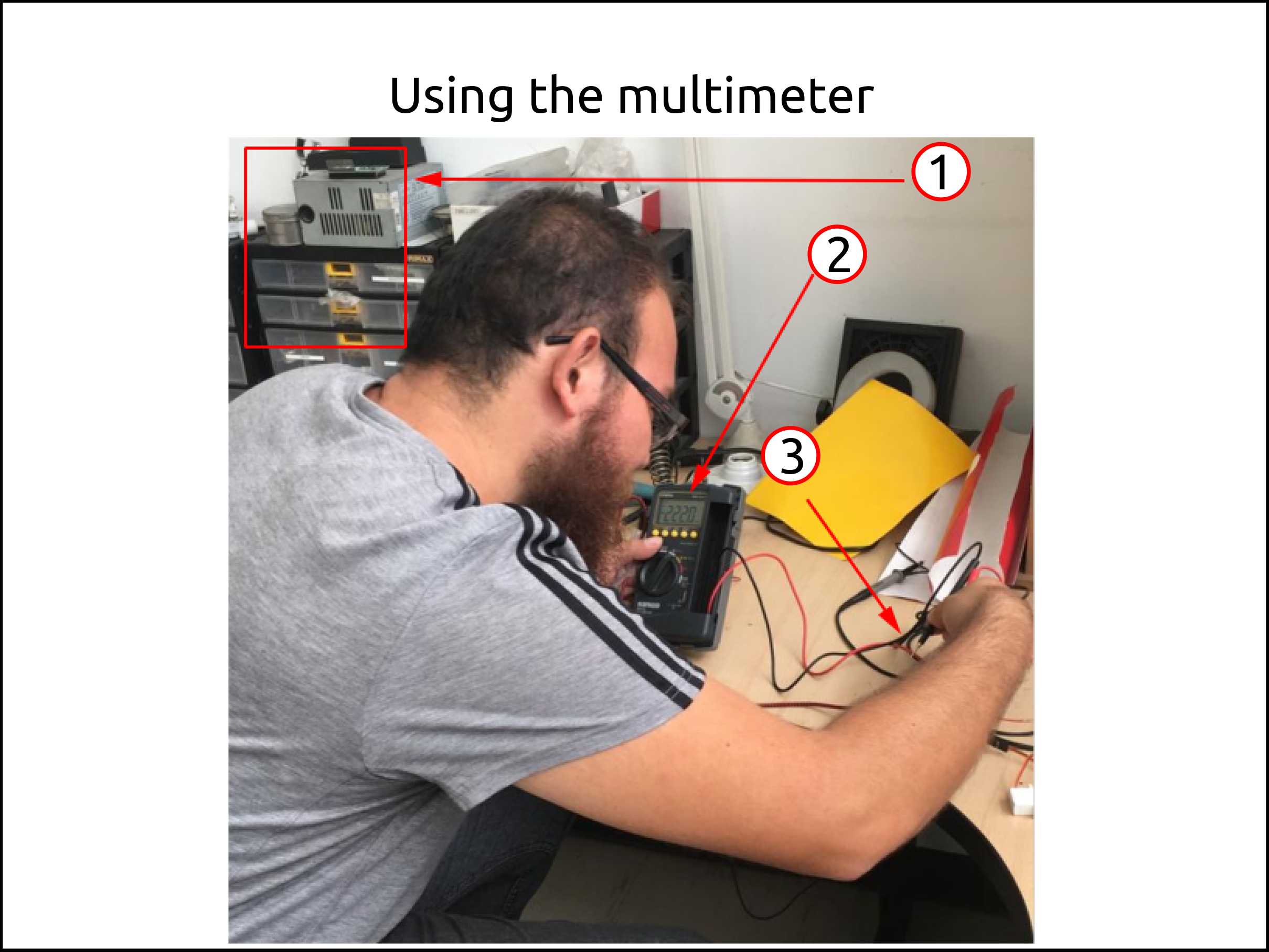
Multimeter
-
Here we see little drawers where are the electronic components sometimes new other components to up-cycle them.
-
Here we see a Multimeter that is a device that helps us to measure different magnitudes mainly voltage, current, resistance and also helps us to check the components if it working well like diodes even our board.
-
This device has two proves with a pointed tip to measure small components and so on. We always have to be careful during the measurement about the polarity or connect in parallel or series depending on the magnitude we want to measure.
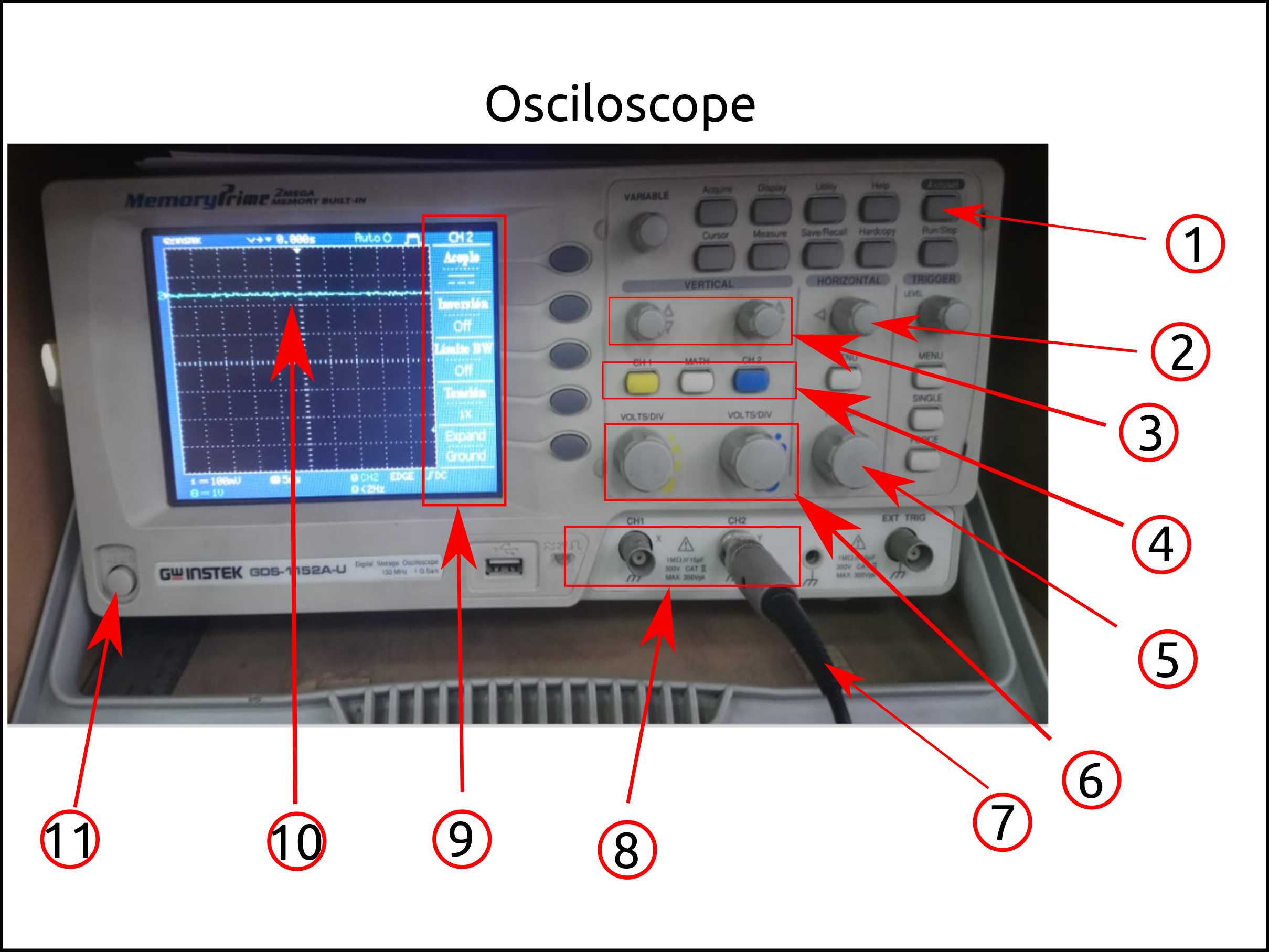
Oscilloscope
-
This is the button called auto-set. If you are beginner this is a helpful button.
-
This knob helps us to position the image in the right place of the screen horizontally. This knob works for both channels.
-
These knobs are for positioning in the vertical axis of the screen. In this case are two of them one for each channel.
-
Here we have a yellow button for turn on/off channel 1 and a blue button to turn on/off channel 2.
-
This knob is the time division tool and helps us to scale up or down the signal horizontally in order to fit the signal in the screen.
-
These knobs are volt division knobs and allow us to scale up an down the signal amplitude in order to see clearly the signal, these knobs work with time division knob.
-
This an Oscilloscope prove and is connected in the channel 2 in this case. This proves has a little switch that helps us to compensate for the signal. If the signal has a good amplitude the switch is placed in the 1X section, otherwise is placed in 10X to amplify the input signal.
-
These two BNC connectors are where the inputs have to be connected in order to measure the signals.
-
In this side of the screen, the Oscilloscope shows us the magnitudes that are capable to measure, like frequency, voltages and so on.
-
This is the signal of channel two of the Oscilloscope.
-
The power button. Do not forget to turn off after using it!
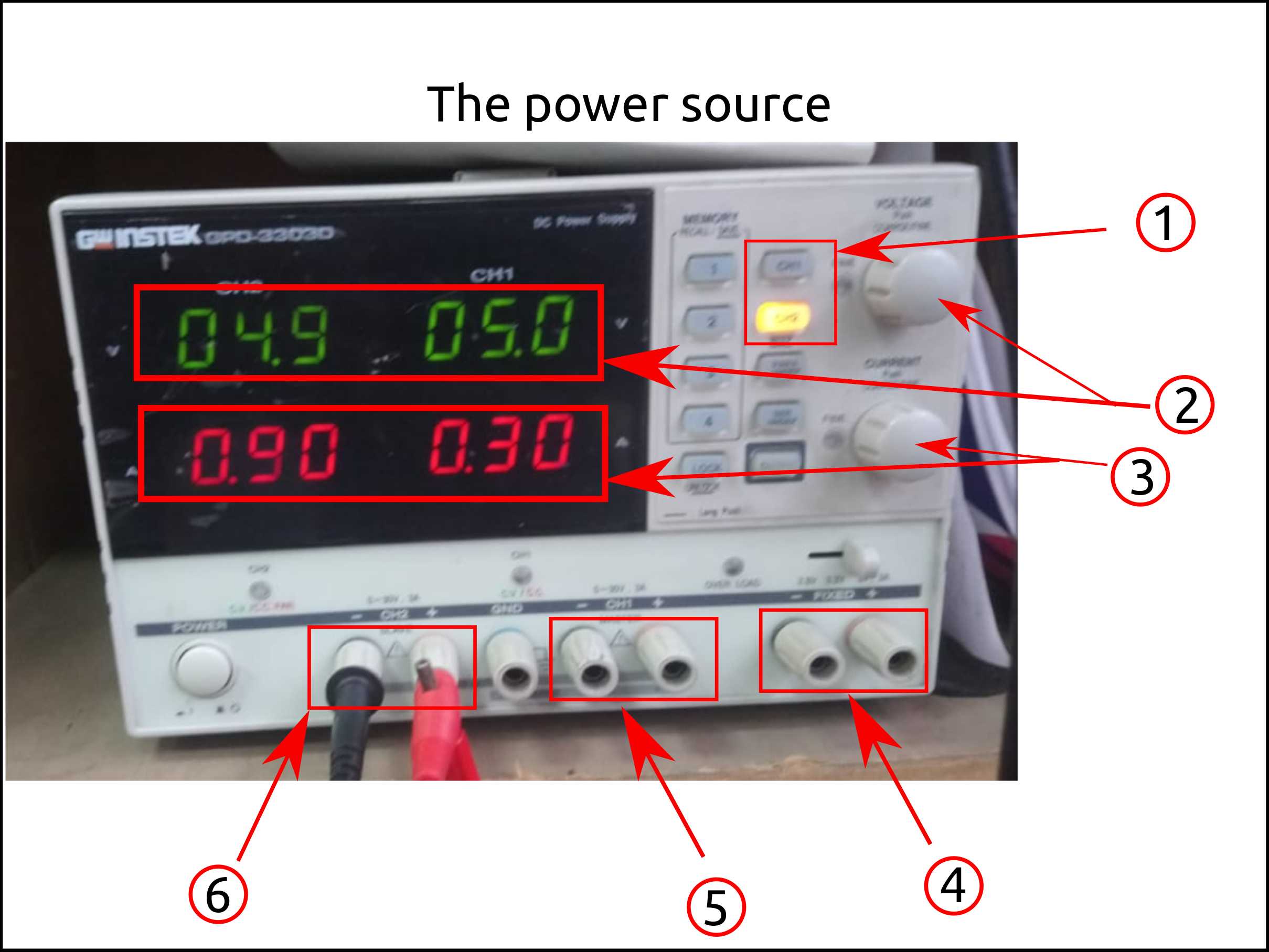
Power supply
-
These buttons are to select which channel we want to use.
-
After choosing the channel you want to work with we use this knob to select the voltage.
-
Like the voltage selector knob, we have a current selector knob, that helps us to select the limiting current in order to protect our circuit.
-
The power source has a fix voltages with a selector switch.
-
These are the connectors of the variable voltages, on the left side, we have the other channel.
-
I order to connect our power source with the circuit we need of these two cables one for positive (usually red) and the negative (usually black).
Faced problems and solutions using the equipment
Problems:
- We tried to see the signal of a functions generator app in android that gets sine, square and triangle signals out the jack connector. We could not see it.
Solution
- In the beginning, we thought the bad connection of our smartphone output but we figure out that the volt division was not the right one, also we changed the channel from the number one to the number two.
Electronic design
Designing the schematic of the circuit
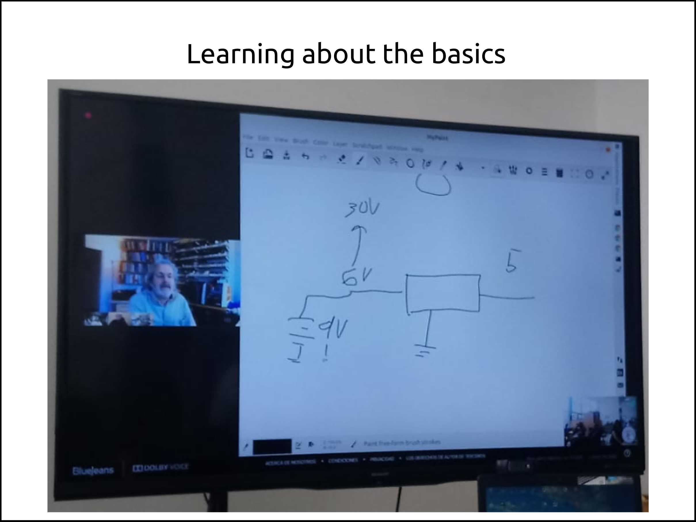
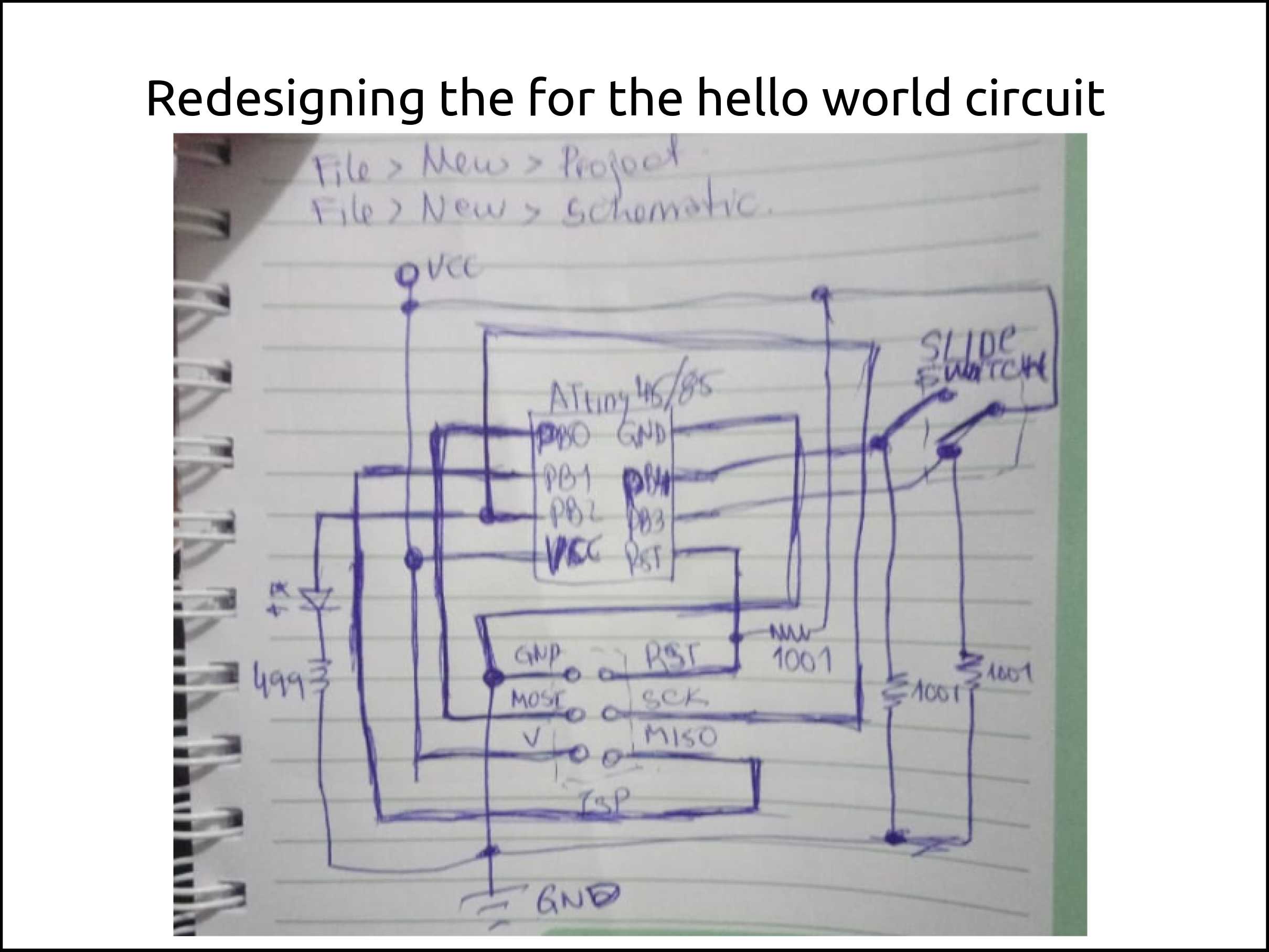
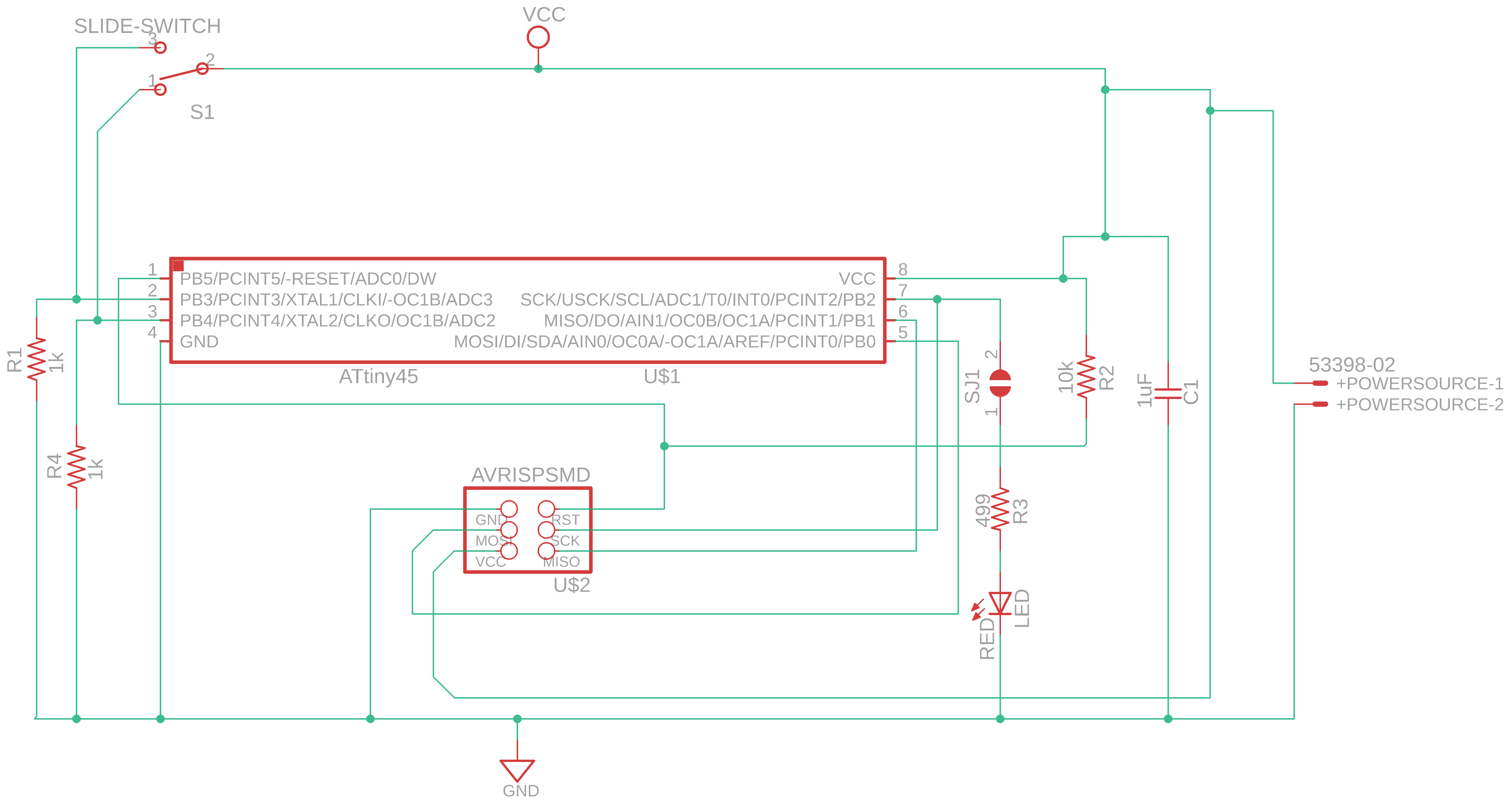
After learning the very basics of electronics I am able to redesign a hello world circuit.
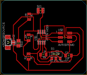
- The circuit that I modified
I take the hello button of the assignment of the input and I draw them from the board and I removed the FTDI connector. I also replaced the button with a slide switch and added a LED.
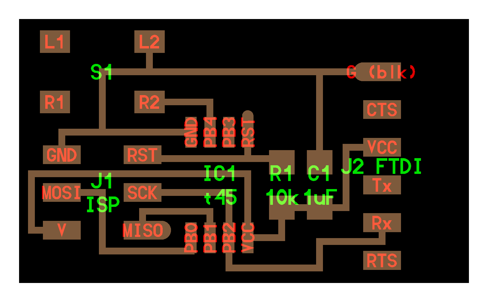
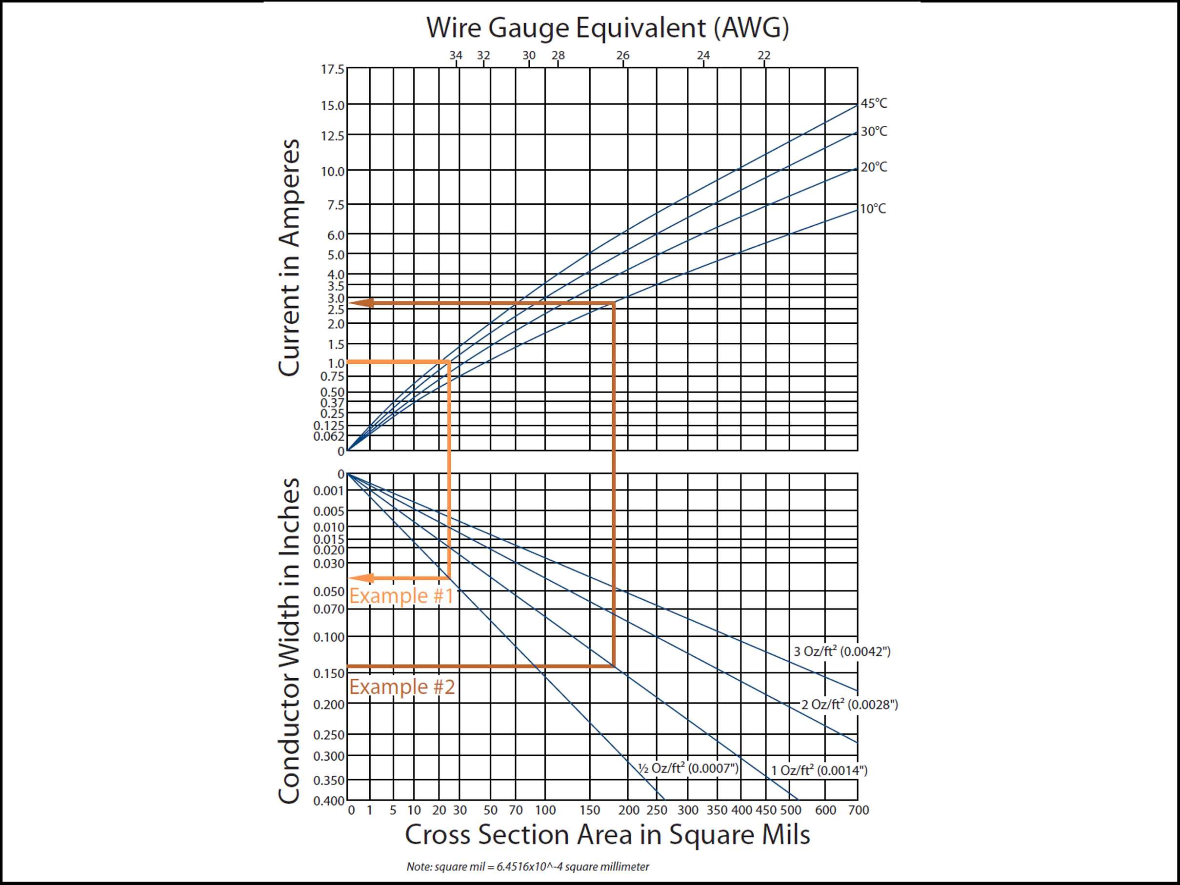
After I finished the schematic was the time of choosing the width of the right trace. If we want to send to somewhere for making professional PCB we have to use the graphics below. In my case my circuit it does not draw too much current I will only need less than 0.005 in but we cannot mill that width of copper. So, that is the reason why I used >=0.012 in in order to obtain a great trace by using CNC machine.
The value I mentioned (<0.005 in) was calculated by using the current that will draw you circuit the temperature of the board (initial temperature not included in the value) and knowing that the thickness of the board is 1 oz / ft2, 305 g/m2, 35 μm
Faced problems and solutions using the equipment
Problems:
-
We have not in stock the button.
-
We have not in stock the ATtiny44.
-
I could not program the board because I put the resistor and the LED on one of the pins used for programming it (SCK).
Solution
-
I used slide-switch.
-
I used the ATtiny45.
-
I redesign the circuit adding a jumper in order to program the board before adding the load on the programming pins.
Using Autodesk Eagle
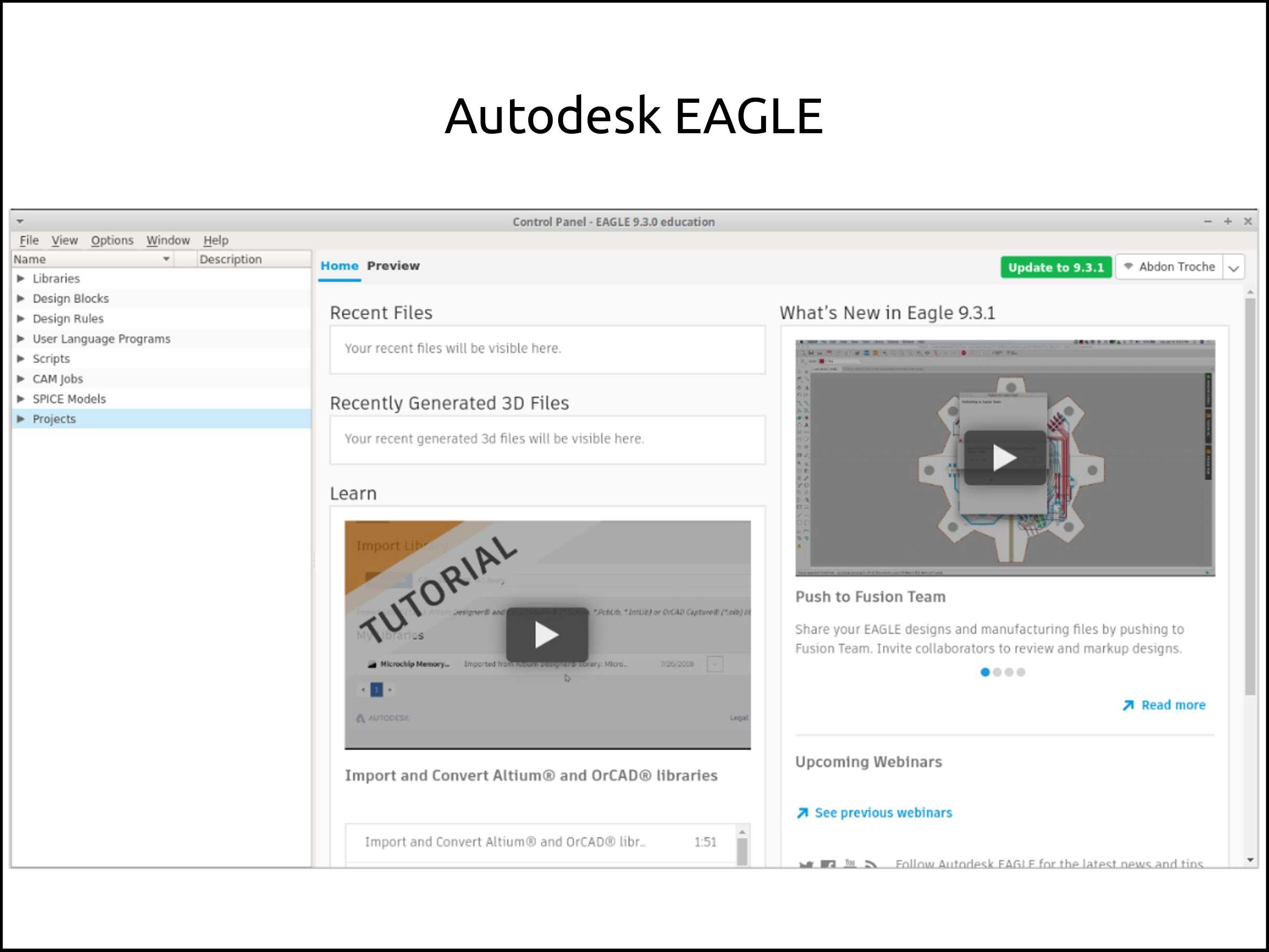
Autodesk EAGLE is an electronic design automation (EDA) software. Enabling a printed circuit board (PCB) designers to seamlessly connect schematic diagrams, component placement, PCB routing, and comprehensive library content.
Steps to use Autodesk EAGLE in Linux
-
Download the program first from here.
-
Extract the compressed file
- Manually doing right click in the file and do extract here
- Through terminal:
tar -xvzf "file.tar.gz"
- Open the extracted folder and run the eagle file using the terminal
sudo ./eagle
- Login to your Autodesk account.
Drawing in the Autodesk EAGLE
This is the environment in the first opening of the software.
I will draw an example circuit that does mean nothing. This is just to show the tools I used in the Autodesk EAGLE.
- First of all, we have to create a new project on EAGLE.
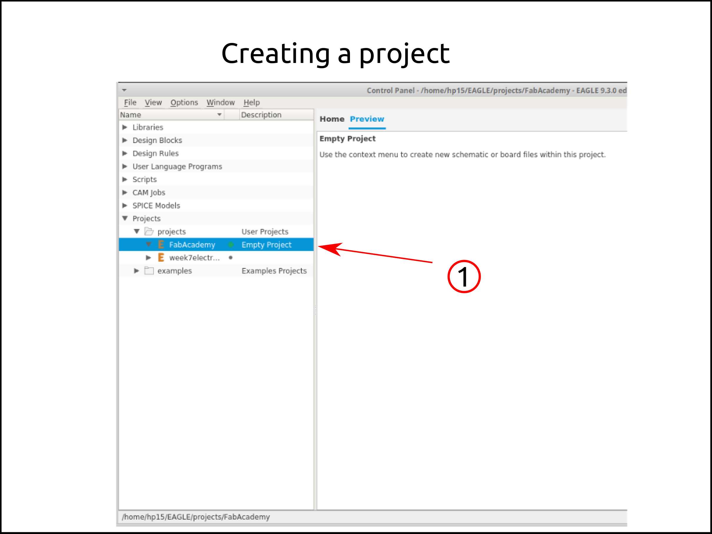
-
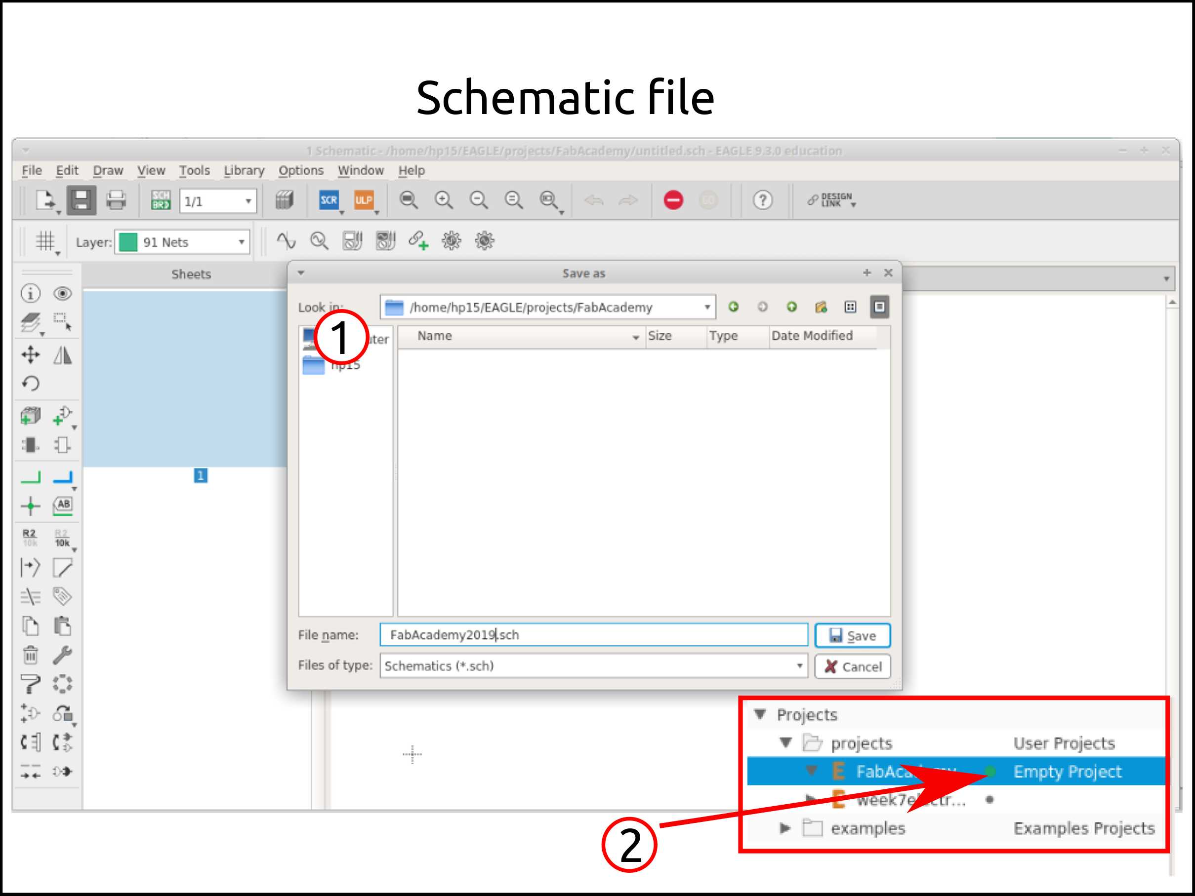
I created a new schematic.
-
The green dot means if the project is active or not.
-
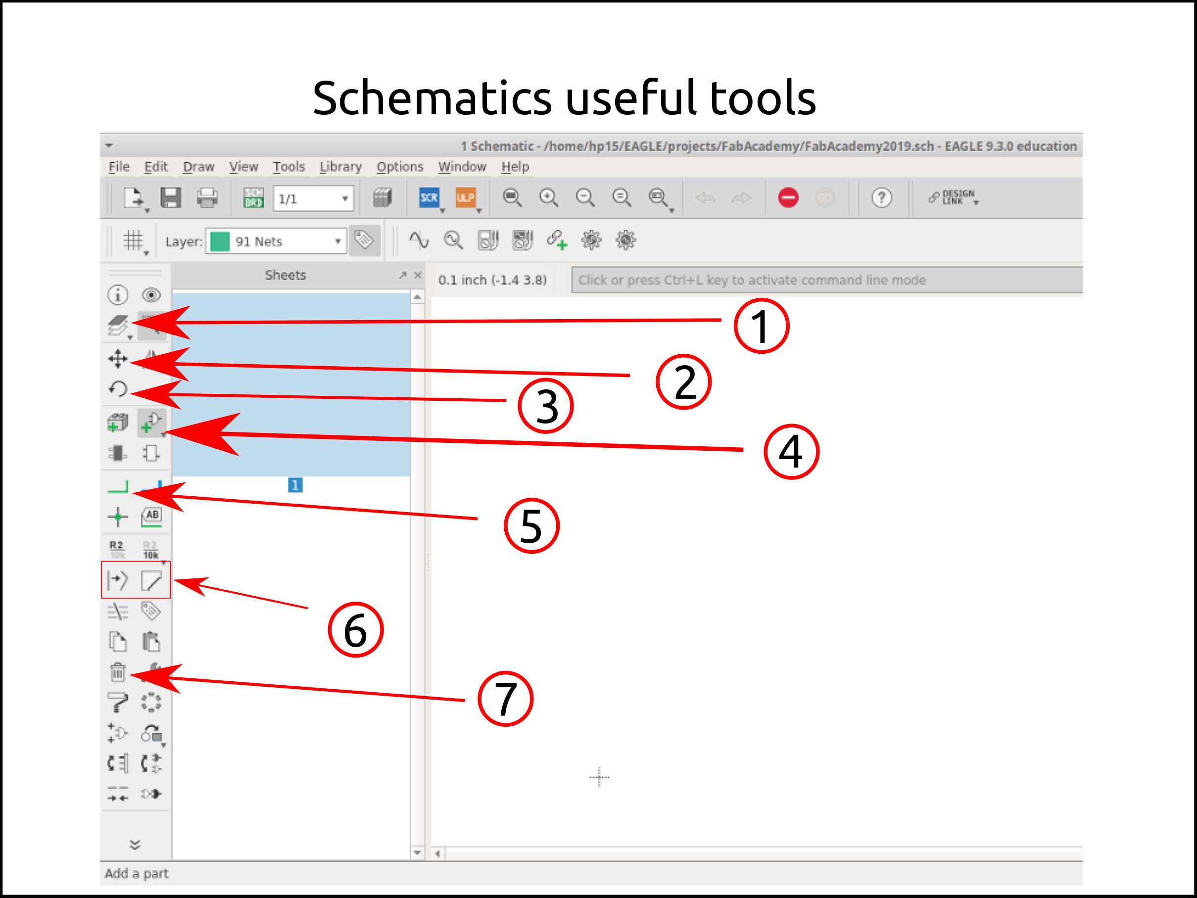
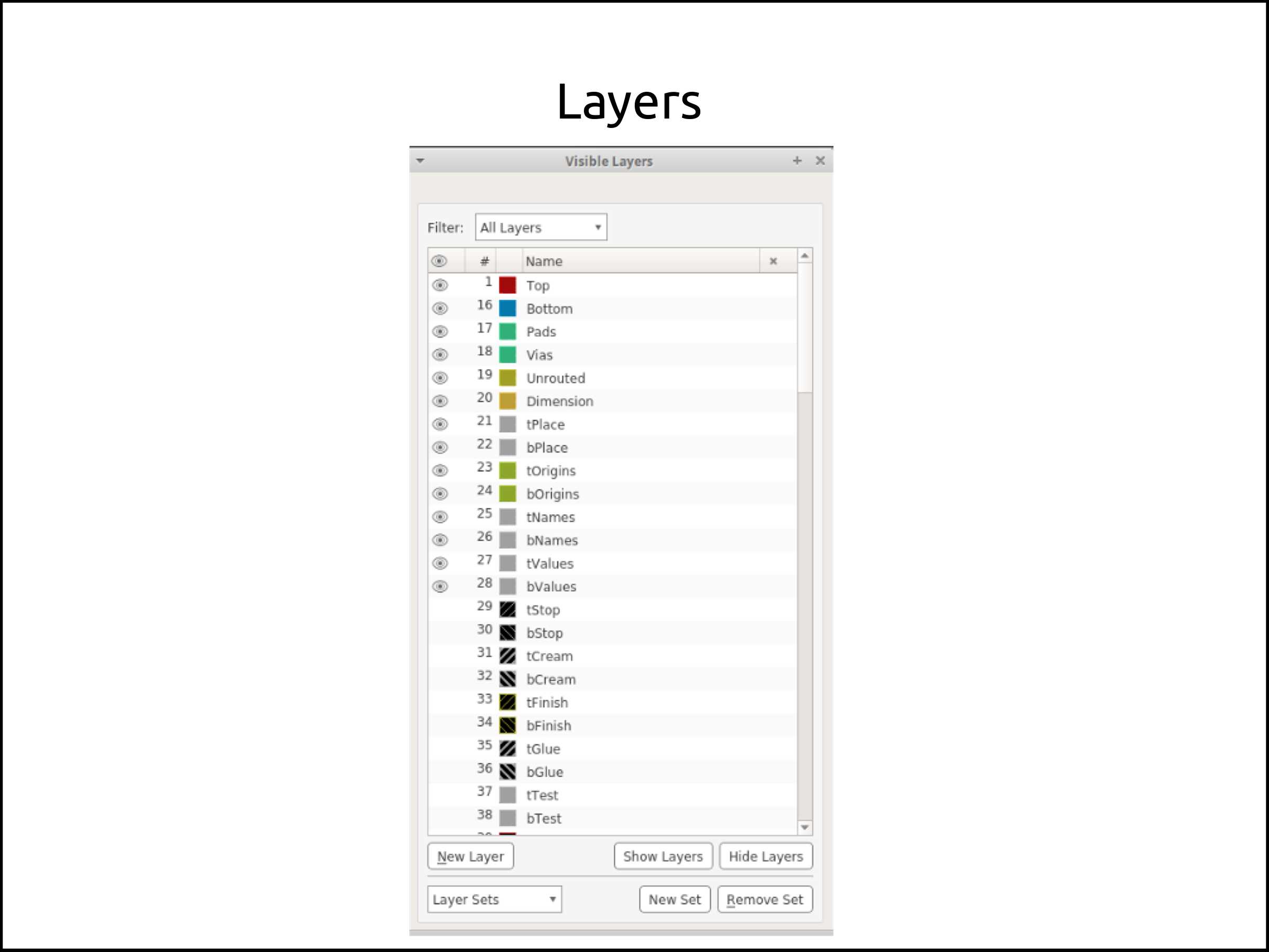
This is to manage the visible layers that you want to see during the design.
-
This is for moving objects whether parts or traces.
-
This is for rotation of the objects, traces, and parts.
-
With this, we can add a new component using the libraries.
-
This is to make the connections between the components.
-
These help us to modify the connections.
-
With this, we can delete the elements.
-
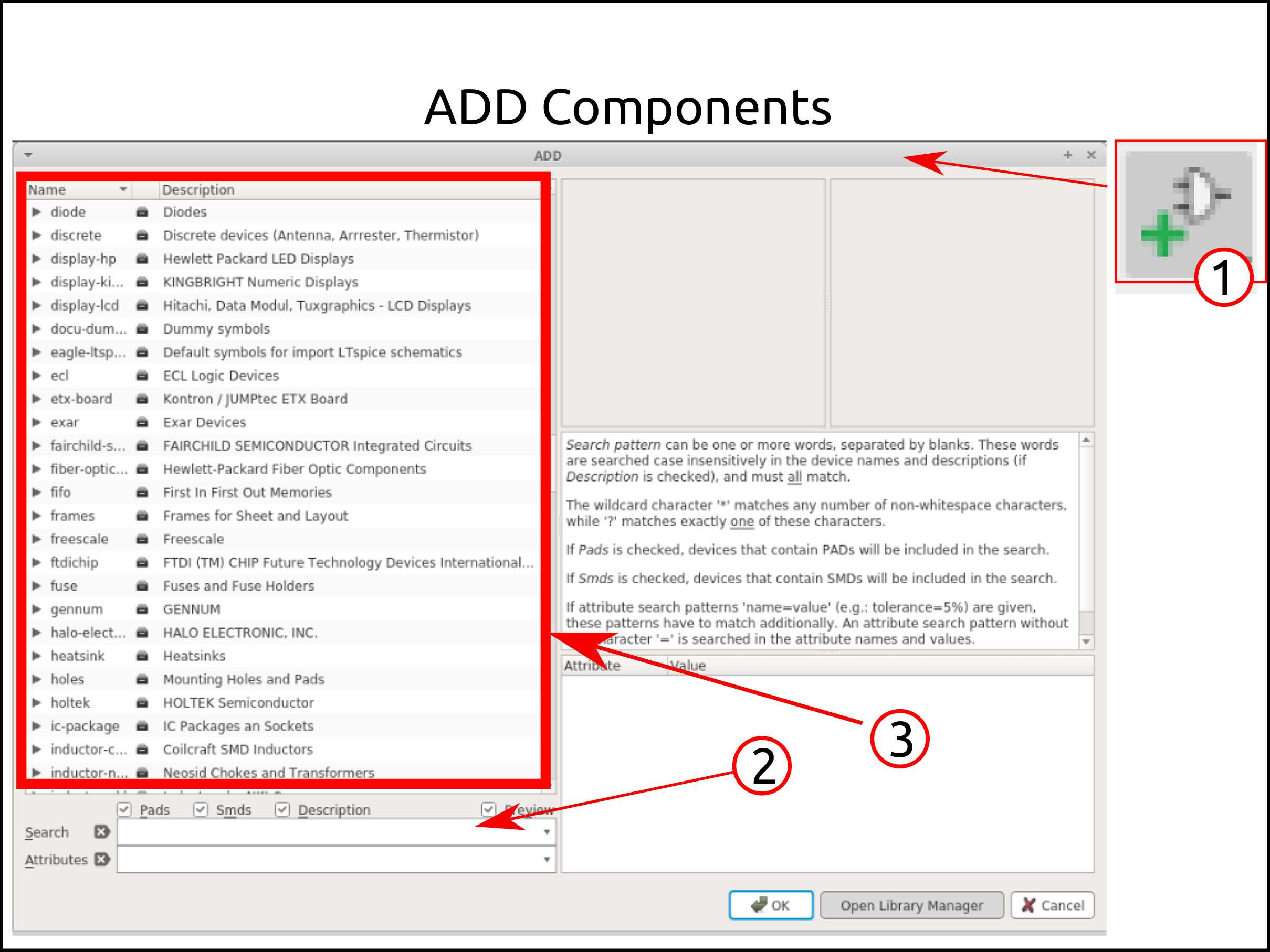
After clicking on add components pop-ups a window showing the active libraries.
-
Active libraries.
-
Search tool. Advance Search tool below.
-
Open the library manager.
-
Change the tab from In design to In use.
-
Click on browse.
-
Go to the Fab Lab library and click open.
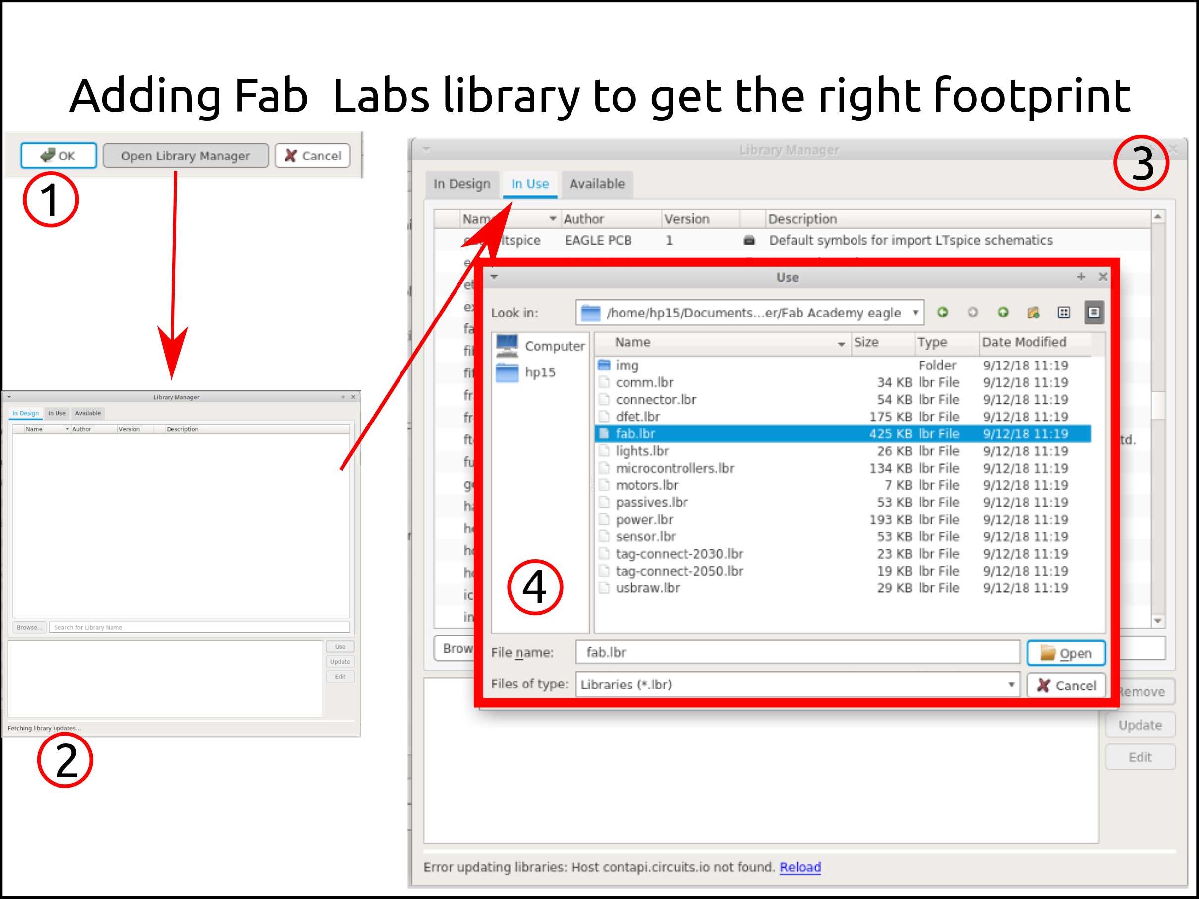
- So, now the library of our interest it appears on the active libraries, that means that is an hour to select the needed components.
-
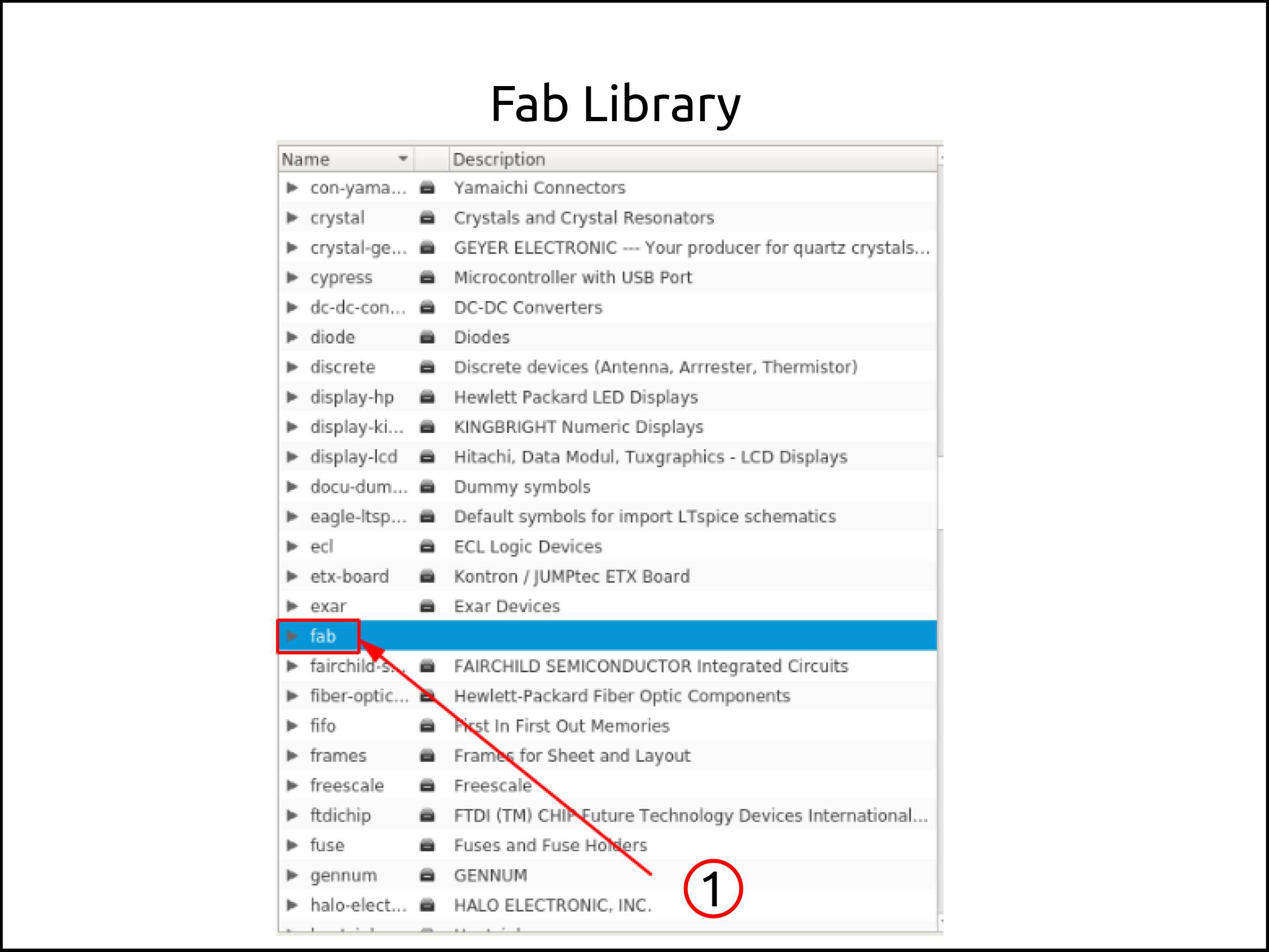
First, you have to search the library of your interest, in this case, is called fab.
-
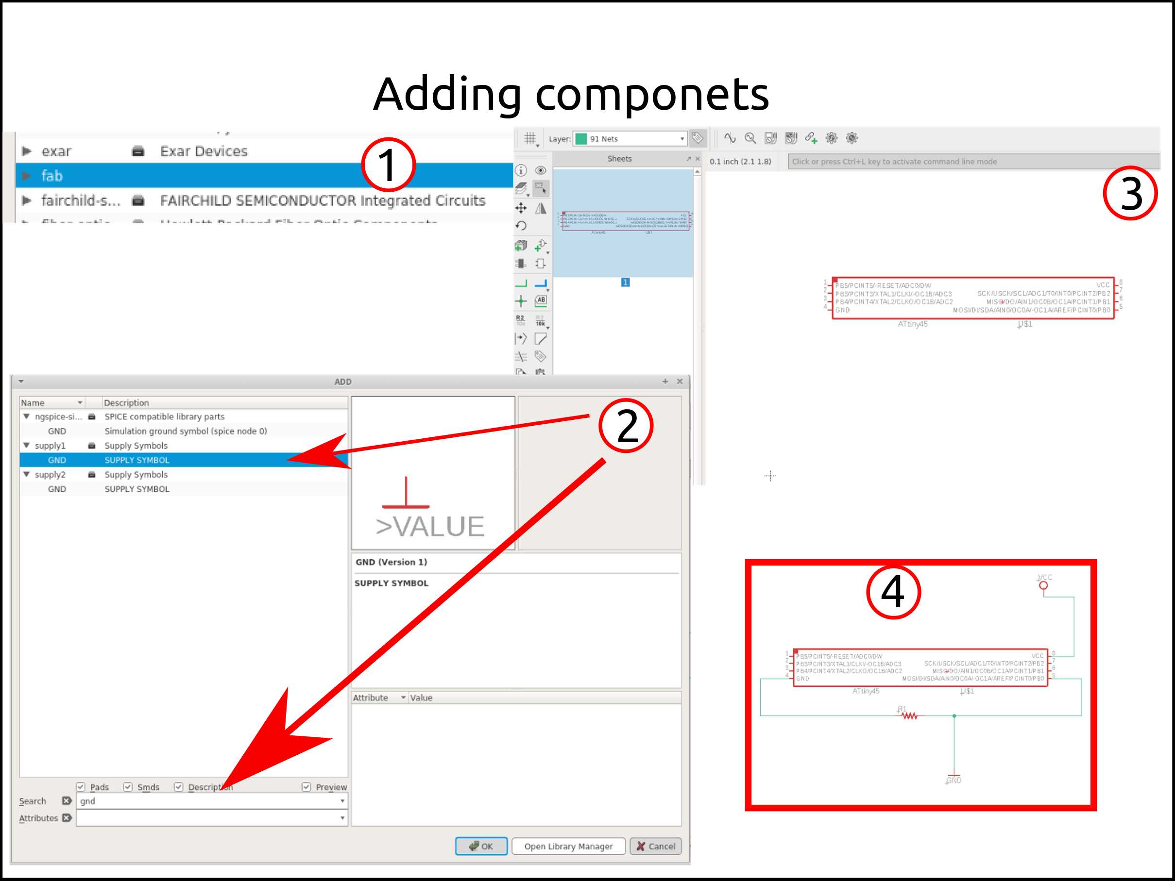
You can search manually the components or by using the search engine.
-
After you find the component you want selected press enter and then click on the workspace the quantity of the same component you need. After press escape to come back to search for another component.
-
This is how looks my example after I finished. Can be all connected or labeled to the connection.
-
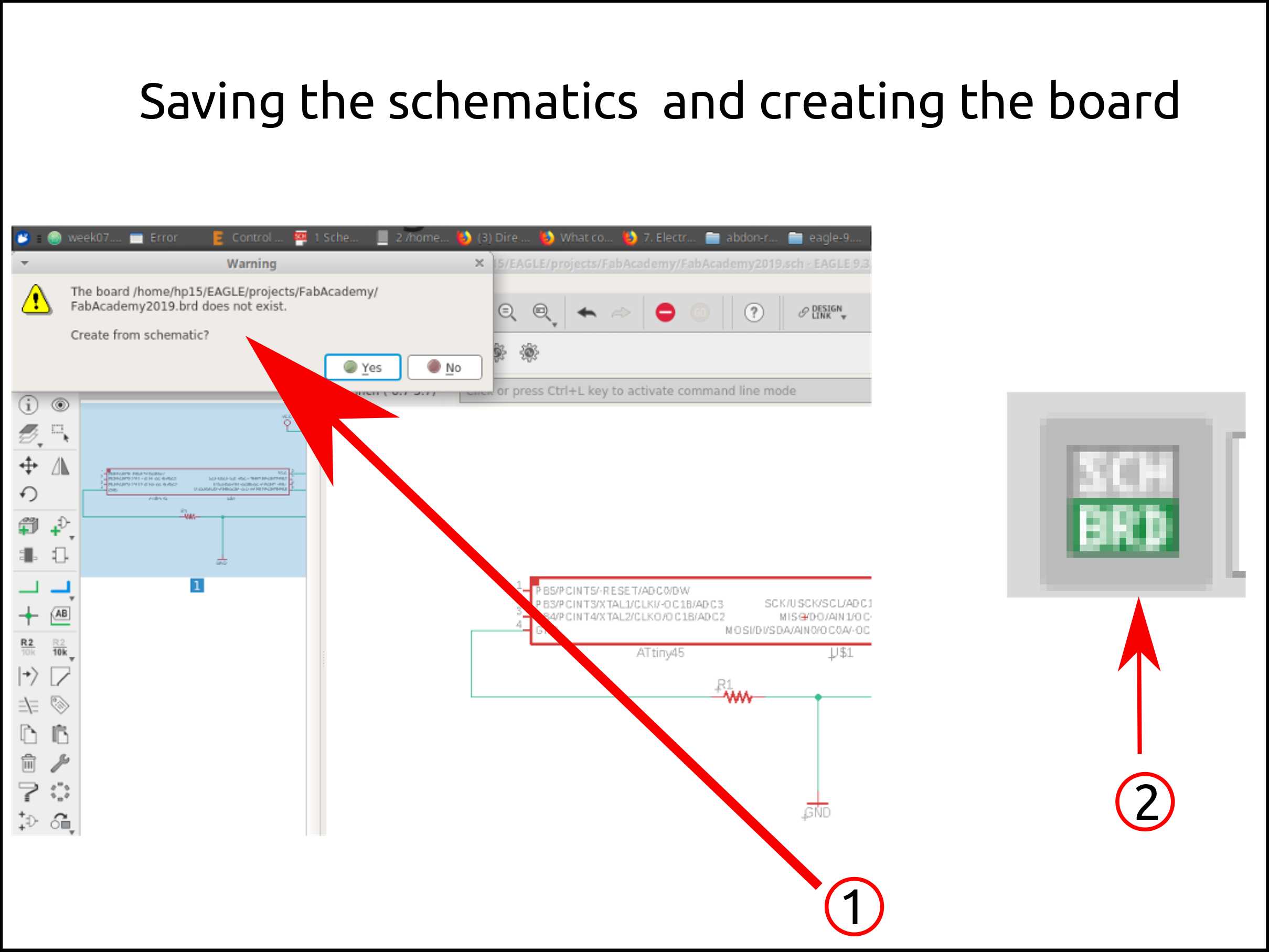
To do the board we have to click in the icon of the number two, and will pop-up a window asking you if you want to create a board from the schematic, press yes.
-
This is the icon to click in order to create the board.
- This is how it will appear the environment to draw the board.
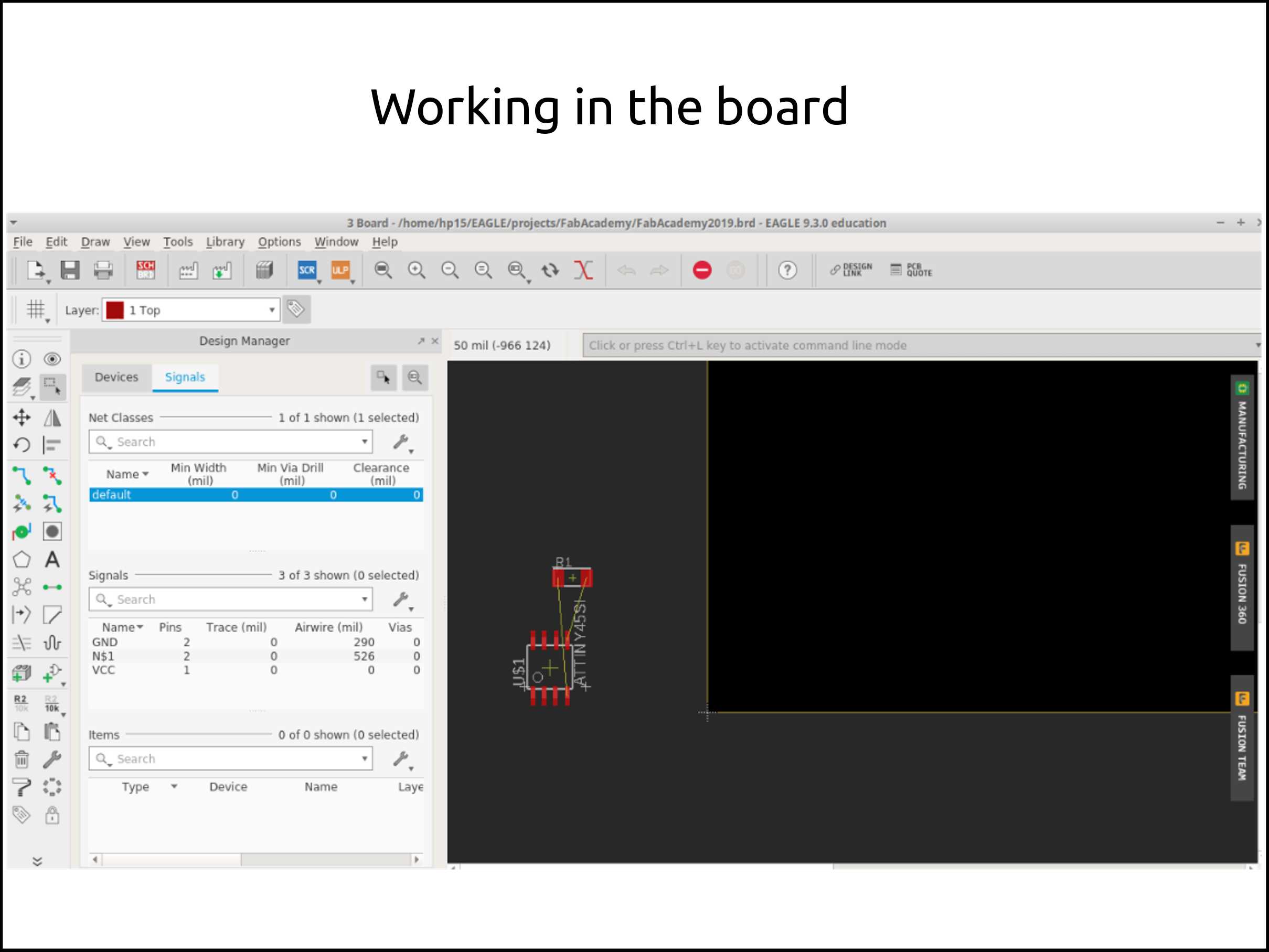
-
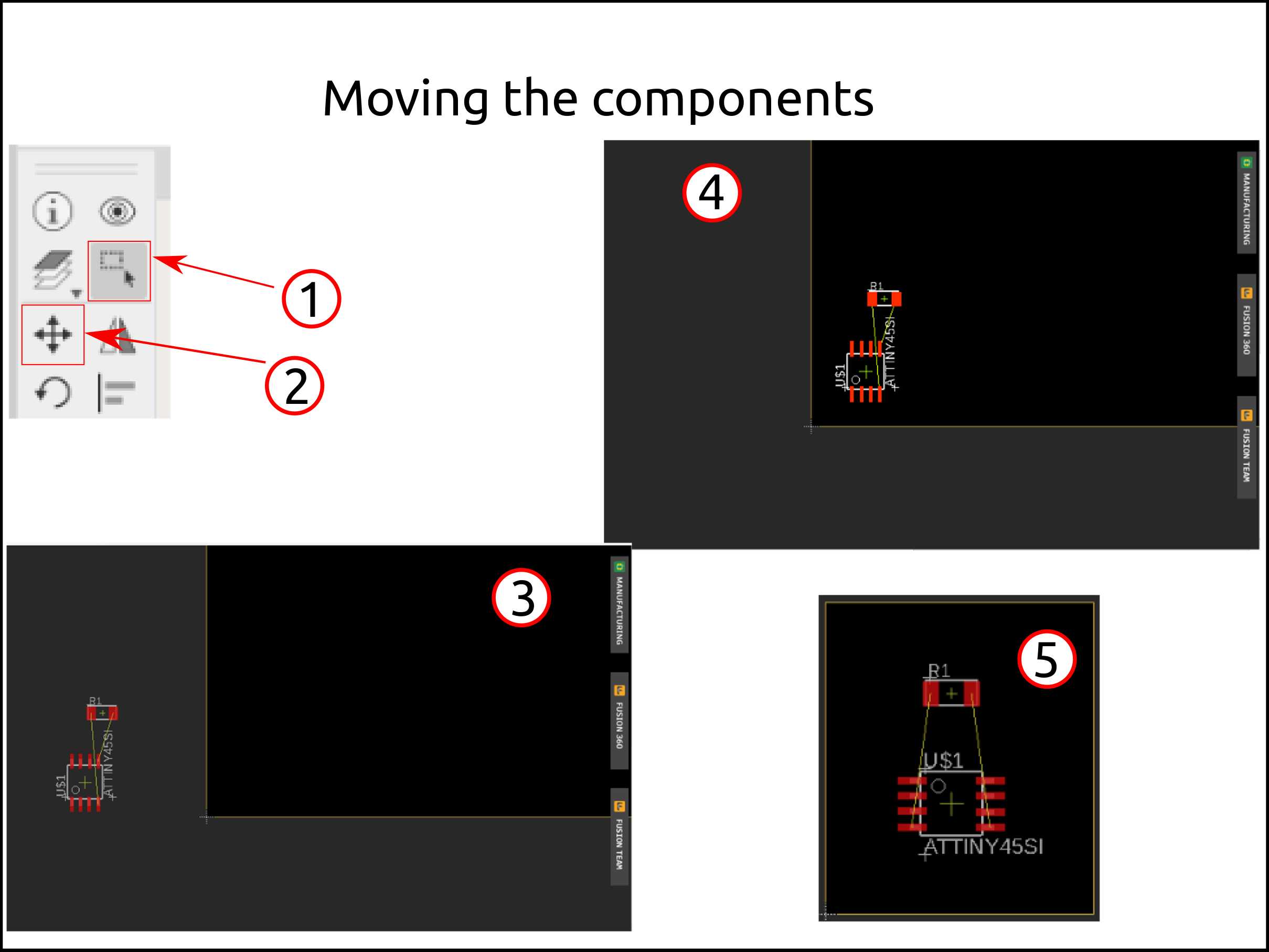
In order to move the components first, we have to use the selection tool.
-
Then with the move tool move the components as a group.
-
The components are selected when is with a bright red.
-
Here I show how it suppose to be the components.
-
Finally, with the move tool resize the background. This last step is very important in order to get the right size of the export monochromatic image for generating the code using MODS or FABMODULS, in my case it does not matter because I will generate the CAM job, in order words, the Gerber files.
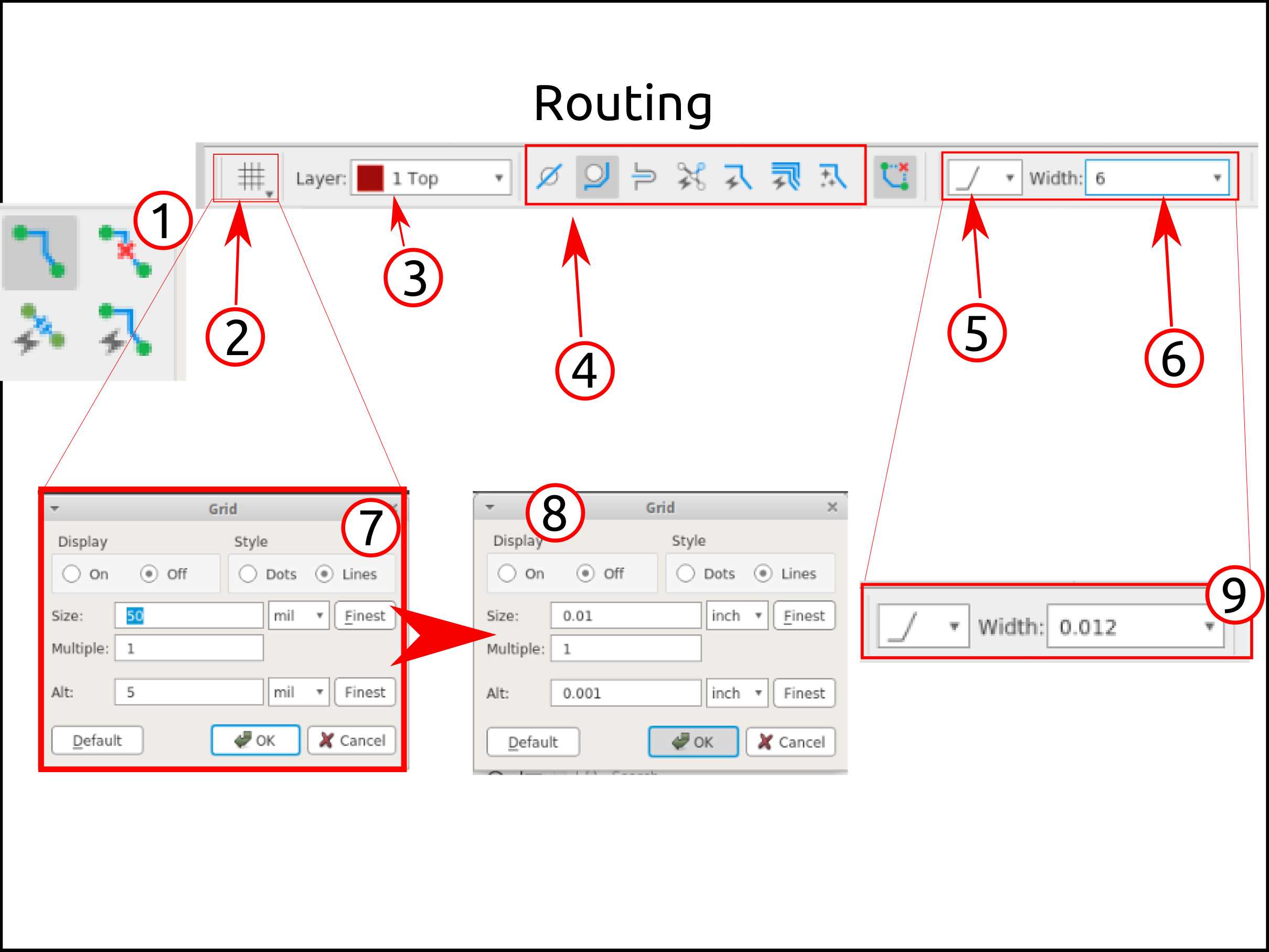
-
These are the routing tools.
-
After pressing the routing tool some new parameters. Here you can turn on/off the grid and modify it, like the size of the square.
-
Here you can see what layer you are working with.
-
Here you can choose the type of routing you want to use. I used to use the interactive routing that is by default.
-
Here you can choose the type of the trace corner shape you want. The rule is to avoid the square corners.
-
Here you can choose the width of your traces.
-
Clicking on the grid icon it pop-ups a window.
-
These are the values I used, these are because it allows you to move freely Through the environment.
-
Here I change the trace width to 0.012 in. If you have more space always choose to increase the trace width to obtain better results in your PCB during the machining.
This is optional, this step is for the creation of the ratsnet.
-
1- This is the normal board.
-
2- Using this tool called polygon we create a closed geometry.
-
5- Correct the errors.
-
4- The resulting board after correcting it.
-
3- Use the tool called ratsnet and pop-up a window, here we choose the signal name, usually it is connected to the GND and the press ok.
-
7- Here we have the result board.
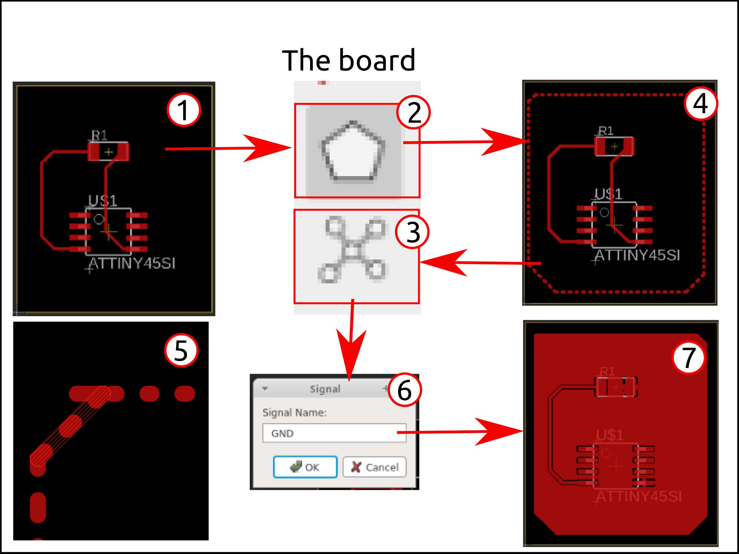
If you want to export to PNG image you must hide the other layers and show only the top layer.
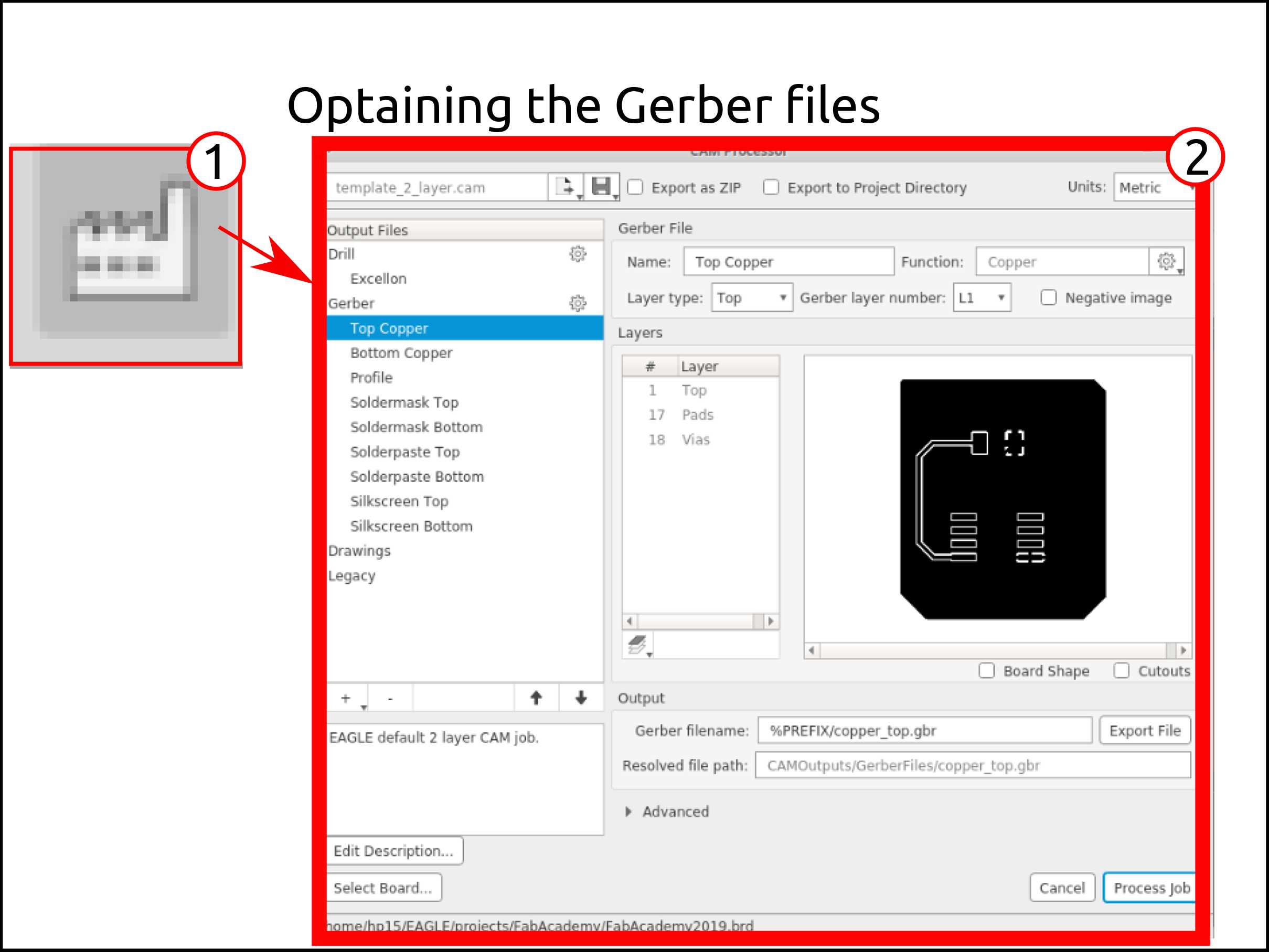
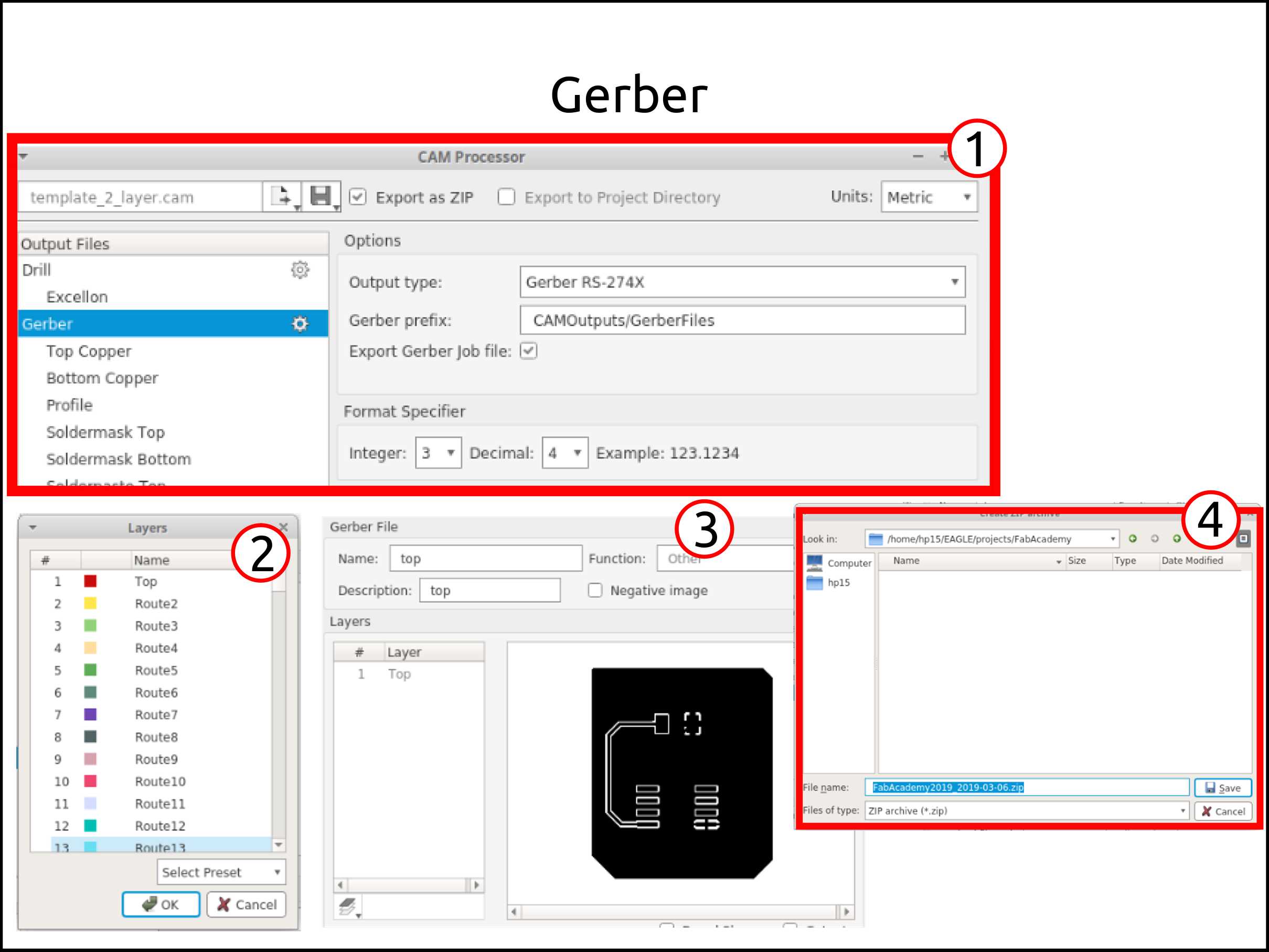
Here we will do the CAM job.
- Clicking on this icon pop-up this window that is of the Gerber generator tool. Keep selected the option Export as a zip.
-
Select Gerber and the tool Gerber RS-274X, and make a new Gerber.
-
Select the layer you want to generate off and press ok, in this case, is the top.
-
Rename them.
-
Select the folder you want to save the generate Gerber in.
Faced problems and solutions using Autodesk Eagle
Problems:
-
I could run properly Autodesk EAGLE because in Linux runs the EAGLE in a sandbox and the problem with this is that I could save my files.
-
I use the auto-routing and the problem with it was the draws traces between the pins of the SMD chip, and that is too thin to mill it.
-
I could not add properly the FAB libraries because in Linux you can add a file in the HOME directory with administrator permission through the terminal.
Solution
-
The solution was to run the EAGLE with sudo ./eagle. Running this way EAGLE disable the sandbox.
-
The solution was to watch how the auto-routing solves the traces and redraw in order to optimize the width of the trace.
-
The solution was open the file manager of Xubuntu using the terminal sudo Thunar, after that you will able to add the libraries in the folders that you create in EAGLE.
Autodesk EAGLE files.
-
Traces
- Cut

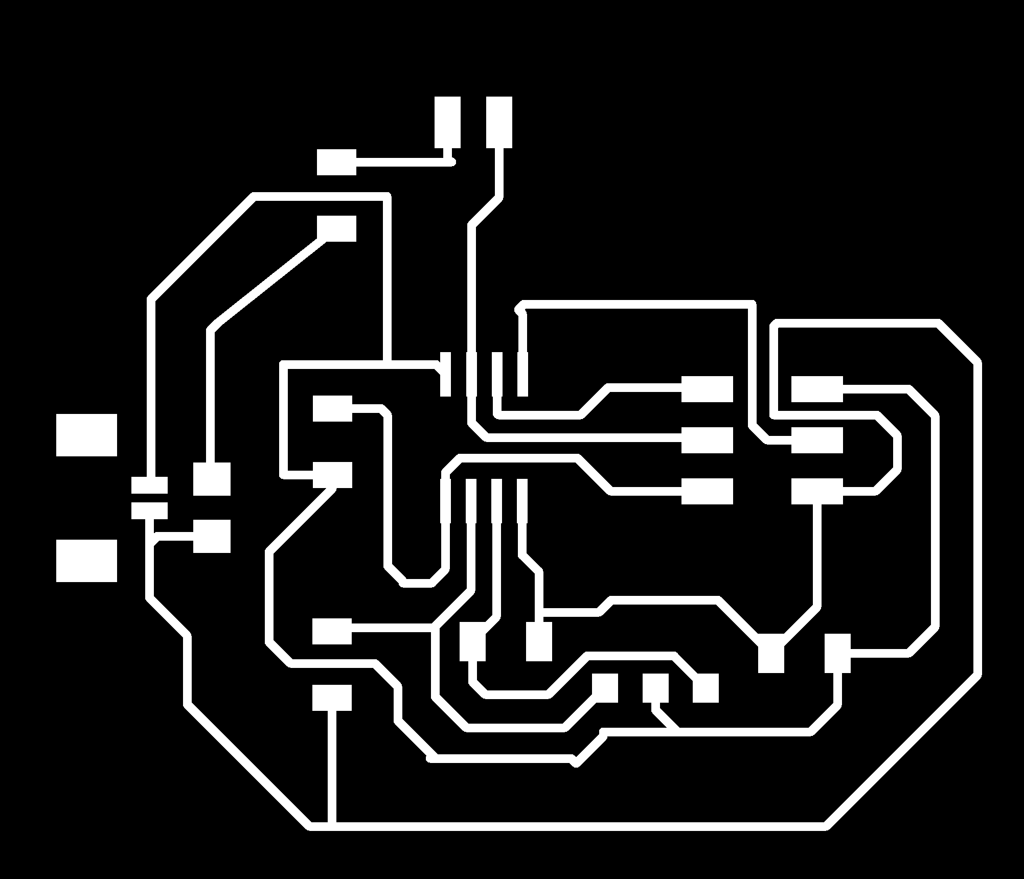
PCB milling
MODS vs FlatCAM
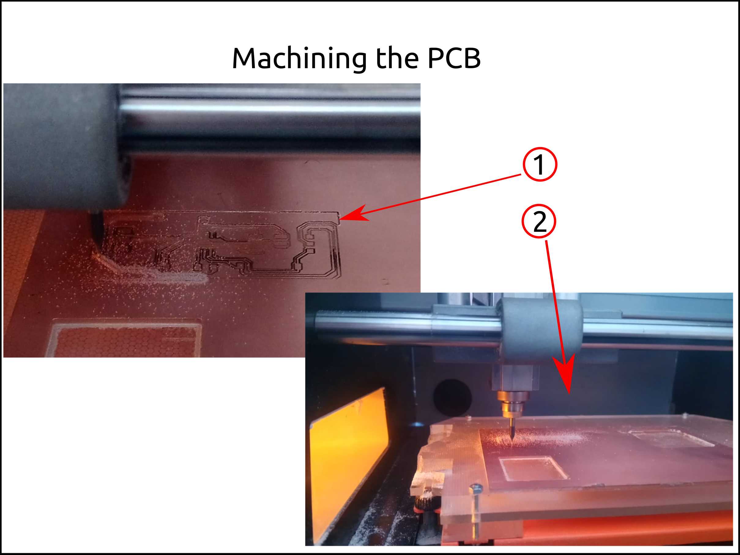
I started the week of electronic production using MODS, and it was a good experience, but that was because I used the Modela MDX-20. After I moved to the SRM-20 because we are 9 people doing the academy I started to see bugs in the MODS. One of them was that I had to download the file generated by the MODS and then send it through the software Vpanel of Roland and it does not work, first moves to the origin and then move to the Z-axis and stops.
This situation makes me feel frustrated and I started to search another way to generate the code for the router machine and I found the software.
I was great to find this software because is free too easy to install and it runs on Linux, Windows, and MAC. Is easy to work with and you can generate fast code for a big range of machines, for example, the Modela MDX-15/20, that only accept RML1 code for machining.
The image below was my first try using the Gcode generate with the FlatCAM.
Using FlatCAM
FlatCAM lets you take your designs to a CNC router. You can open Gerber, Excellon or G-code, edit it or create from scratch, and output G-Code. Isolation routing is one of the many tasks that FlatCAM is perfect for. It’s is open source, written in Python and runs smoothly on most platforms.
Installing FlatCAM
Installing Python 3
Step 1:
sudo apt update
Step 2:
sudo apt install python3-pip
Step 3:
pip3 --version
Installing pip3
Step 1:
sudo apt update
Step 2:
sudo apt install python3-pip
Installing PyQt5
Step 1:
pip3 install pyqt5
Step 1:
Installing FlatCAM
pip3 install flatcam
Generating Gcode with FlatCAM
-
Running FlatCAM
-
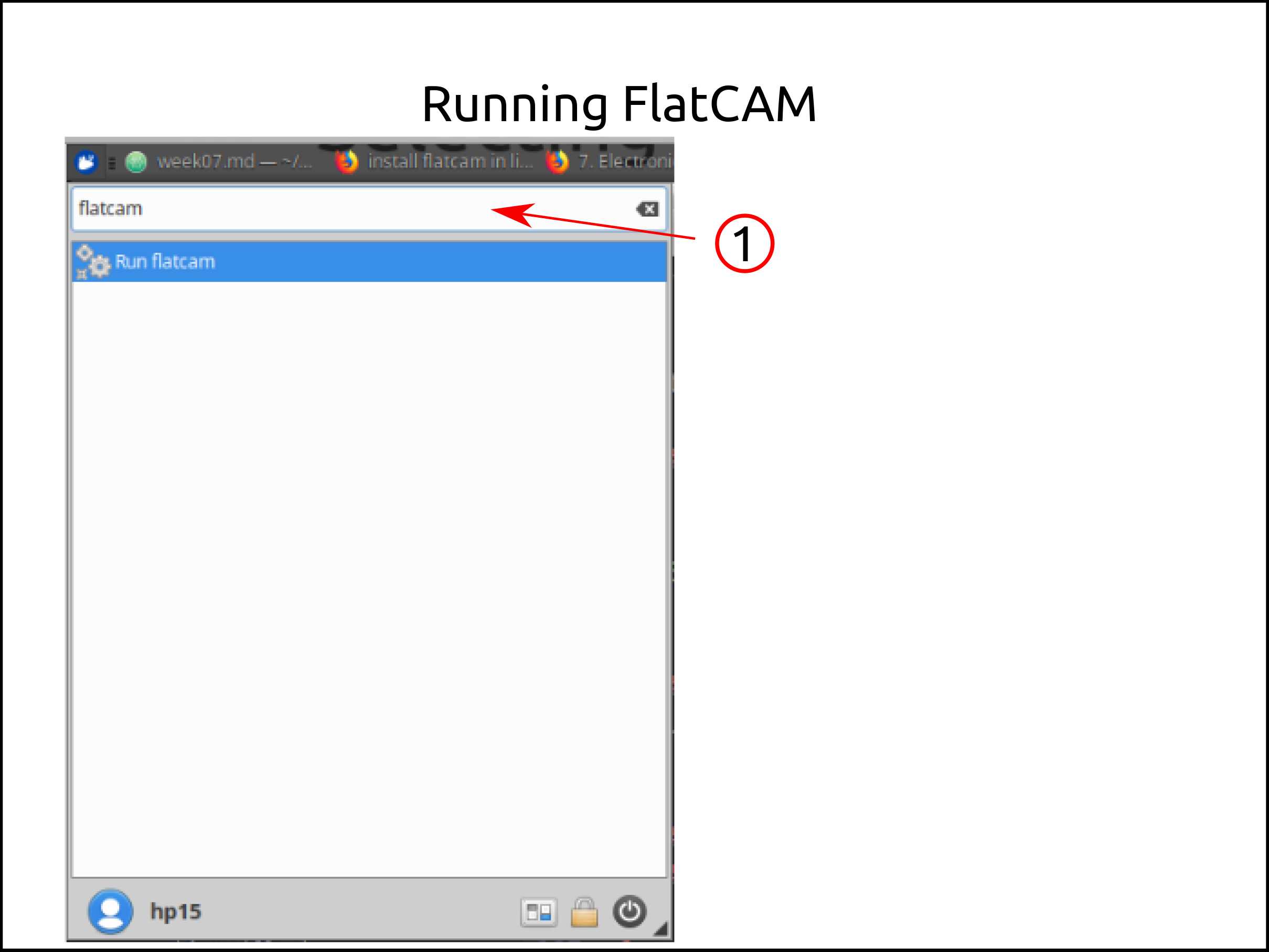
To run FlatCAM you have type flatcam in the software installed searcher and press enter.
-
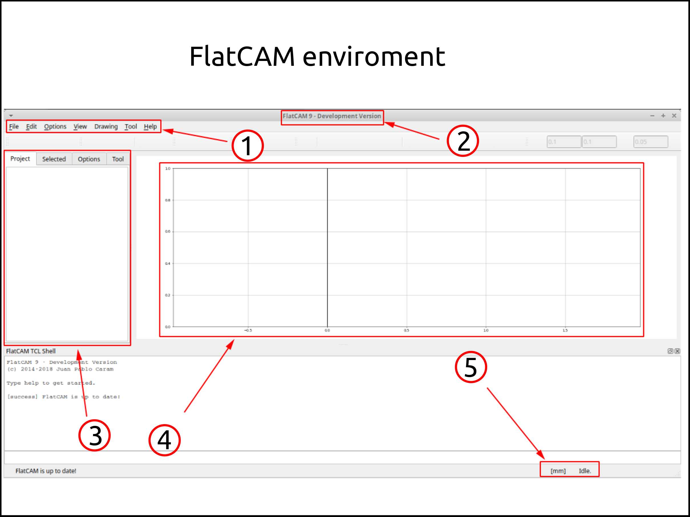
Here you can access all the tools an options that are in the software.
-
Here you can see the version of the FlatCAM that you are using.
-
In this panel you will see all the input files and generated one, also is the place where will appears all the cutting parameters in order to generate the right geometry and CNC job for each machine and tool diameter you have available in your FAB LAB.
-
In this section you will see the imported Geber file and its position in the space, also you will see the geometry and the toolpath of the CNC job.
-
This section is very important because it shows you the current measurement units that you have to choose to avoid mistakes during the routing.
-
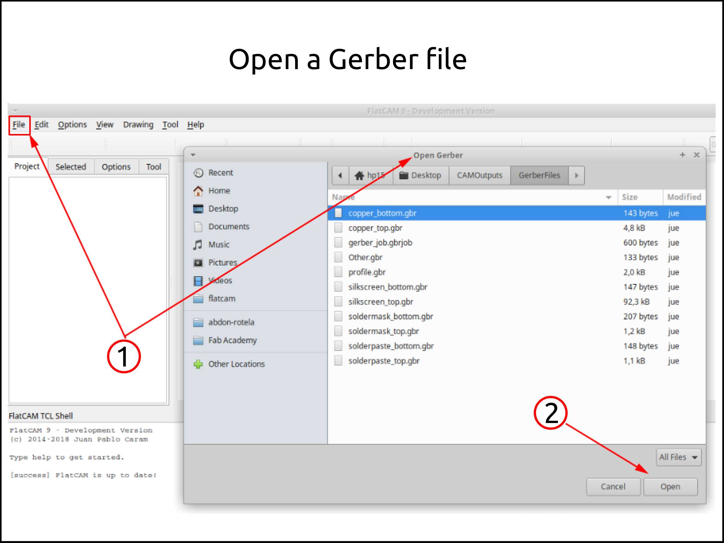
To open the Gerber file that you have generated with Autodesk EAGLE you have to go File/Open Gerber
-
Then you have to choose the Gerber file of your interest and press Open.
-
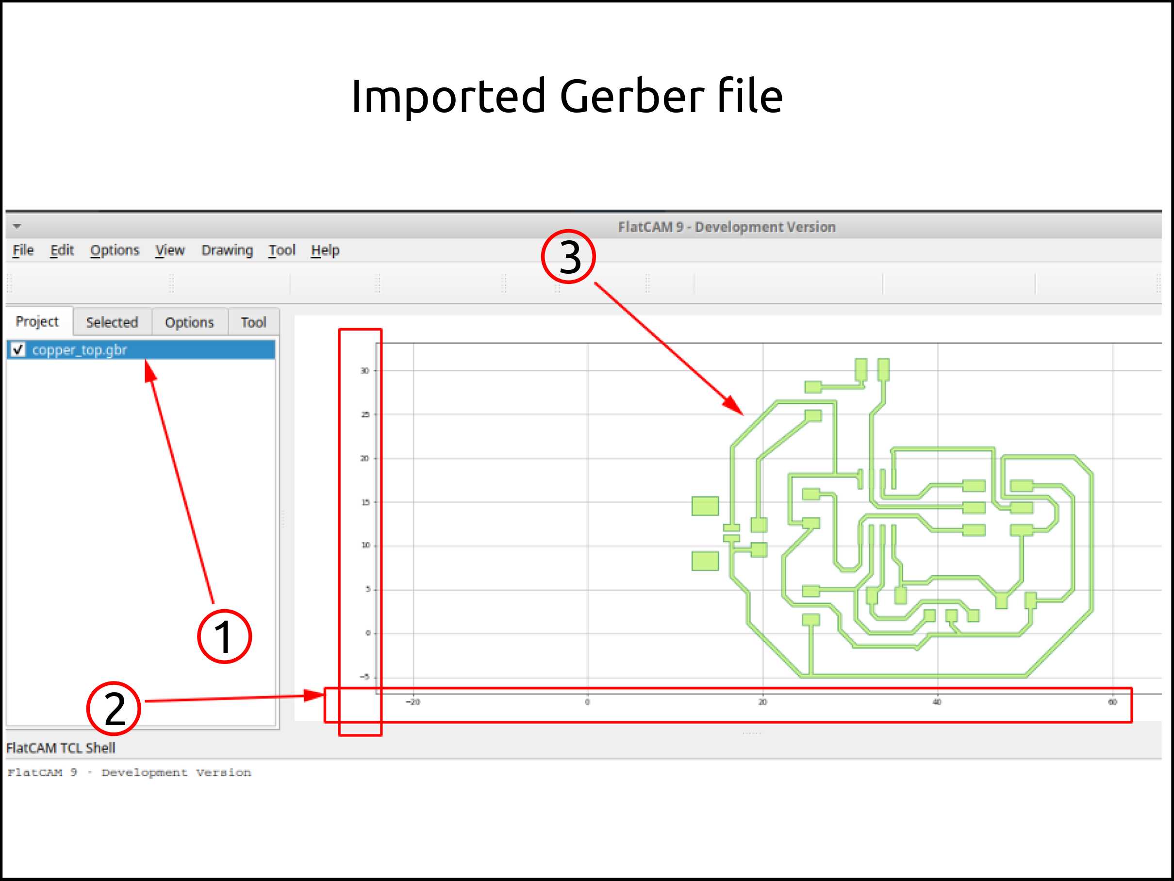
Here it will appear all the Gerber files that you want to generate Gcode with.
-
Here you will see the actual position of your PCB and it allows you to reposition it as you needed.
-
Here you will see the PCB selected.
-
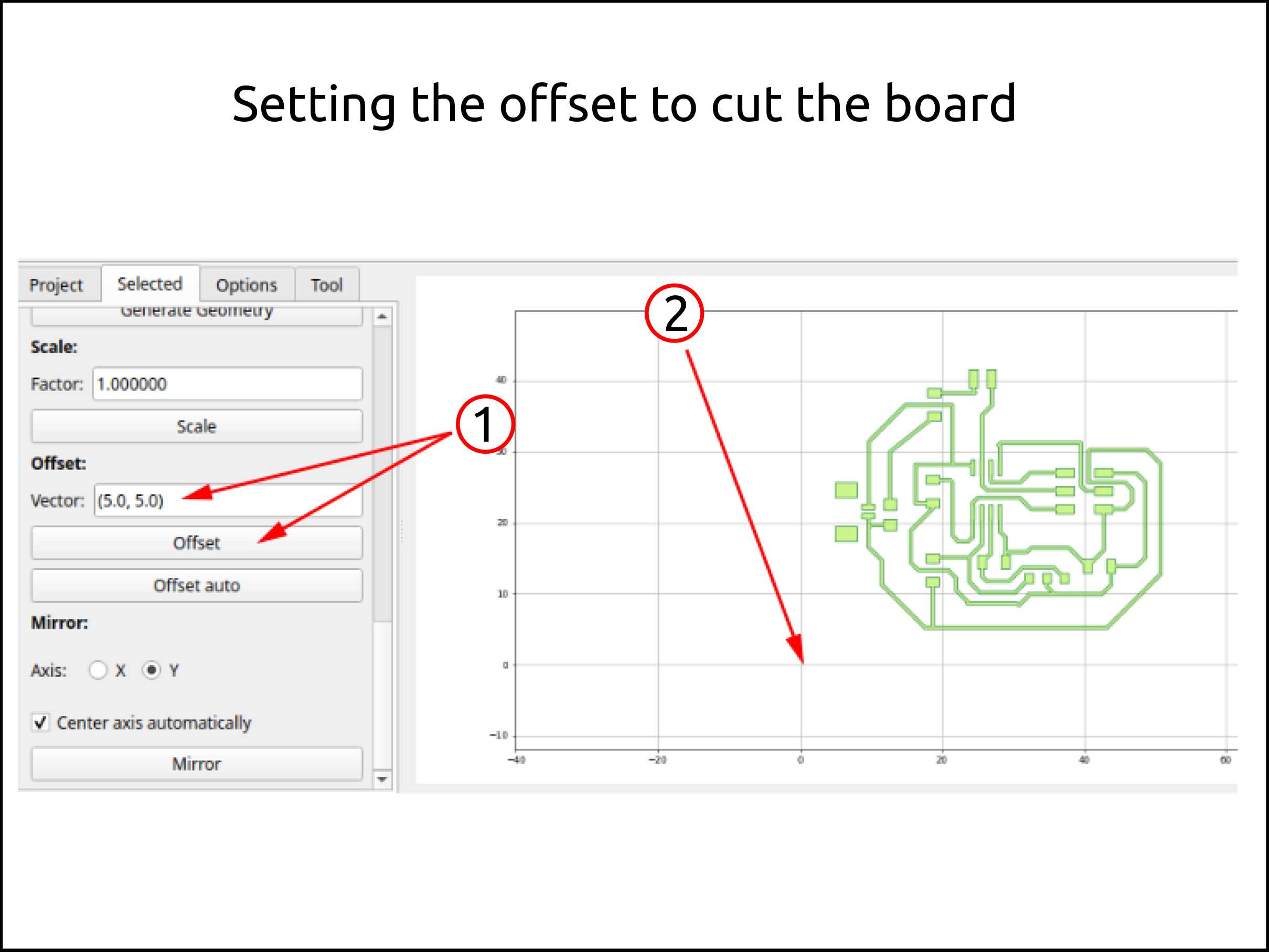
In the section, the vector will appear how much you will offset the origin of your file. Where (x, y) and a positive number to add and a negative number to subtract.They are not coordinates.
-
With this button called offset, you apply the vector values and you will reposition your file.
-
The button called offset auto is helpful because moves your file to the origin, and you can apply a vector value after.
-
Here I show you the origin. You have to care about it to avoid problems during the cutting, in other words, collisions because of the wrong origin.
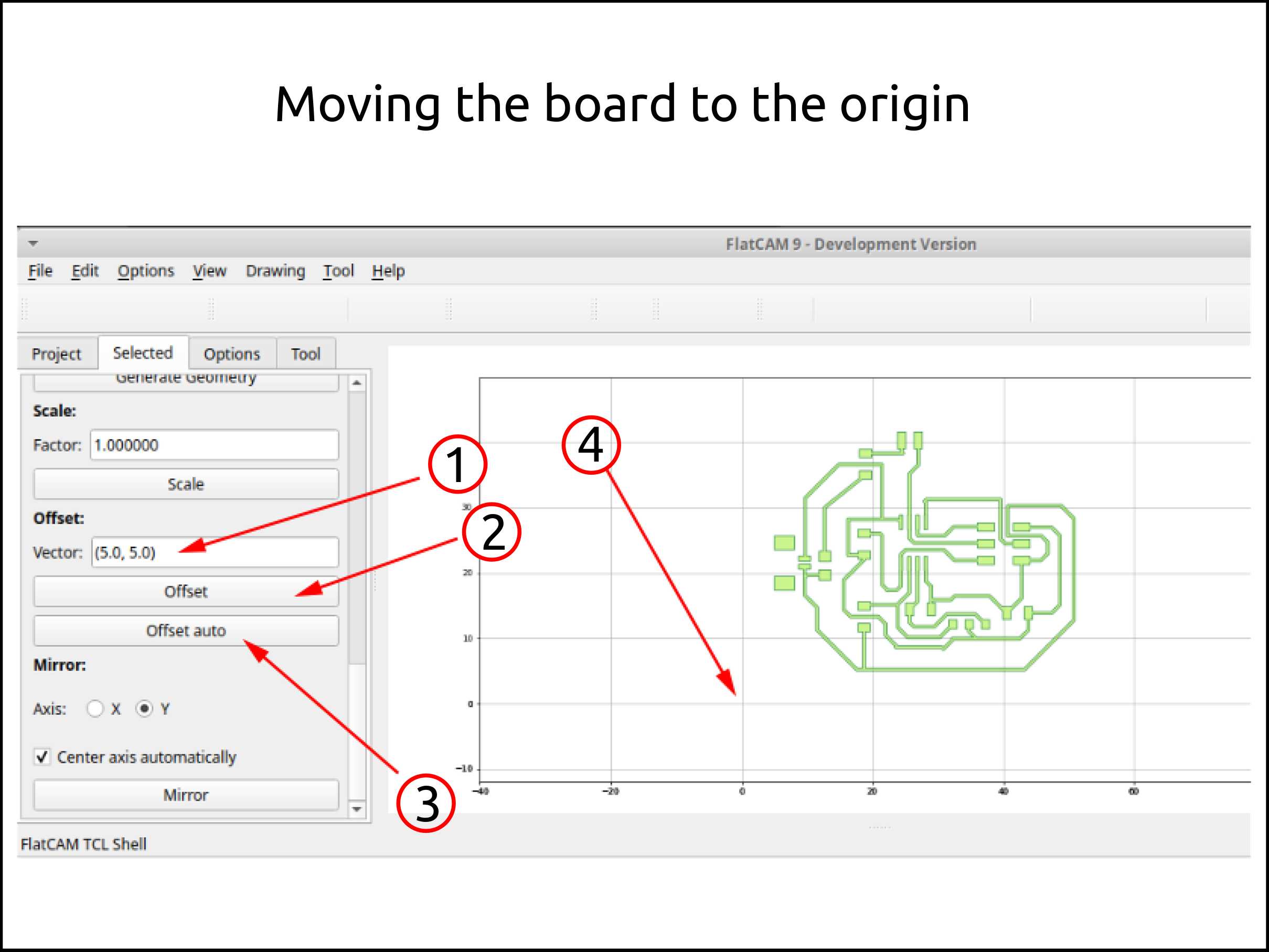
-
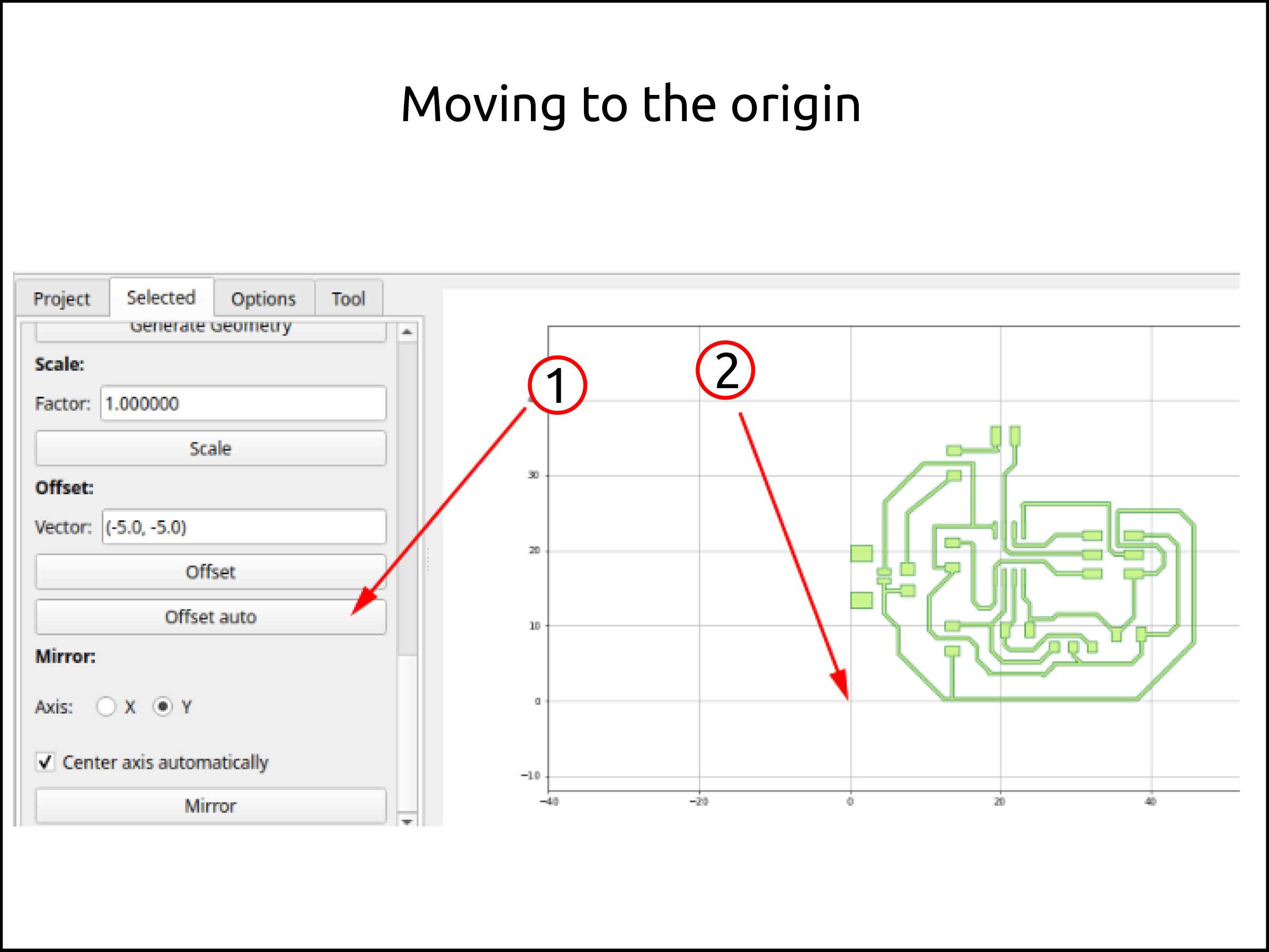
Pressing offset auto.
-
The new position of your image.
-
Setting a new position with the vector and pressing offset to apply it. Is very important to give clearance to your image from the origin in order to cut the board after.
-
The new position of your image.
-
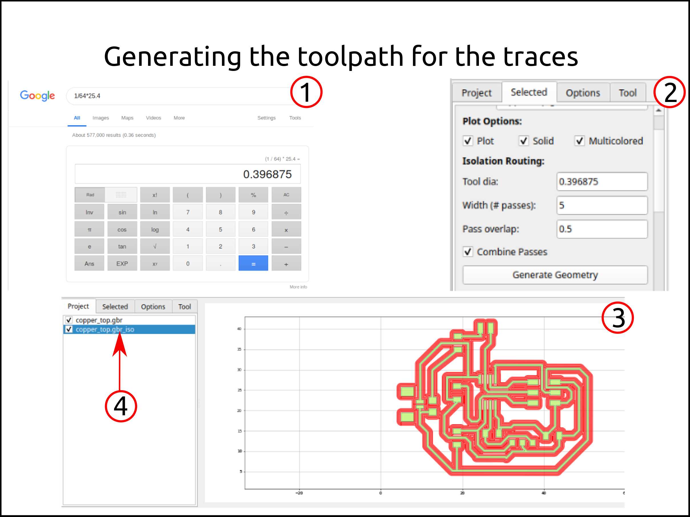
Because I am using millimeters in the FlatCAM and my tool diameter is in inches I convert the tool diameter from 1/64 in to 0.396875 mm.
-
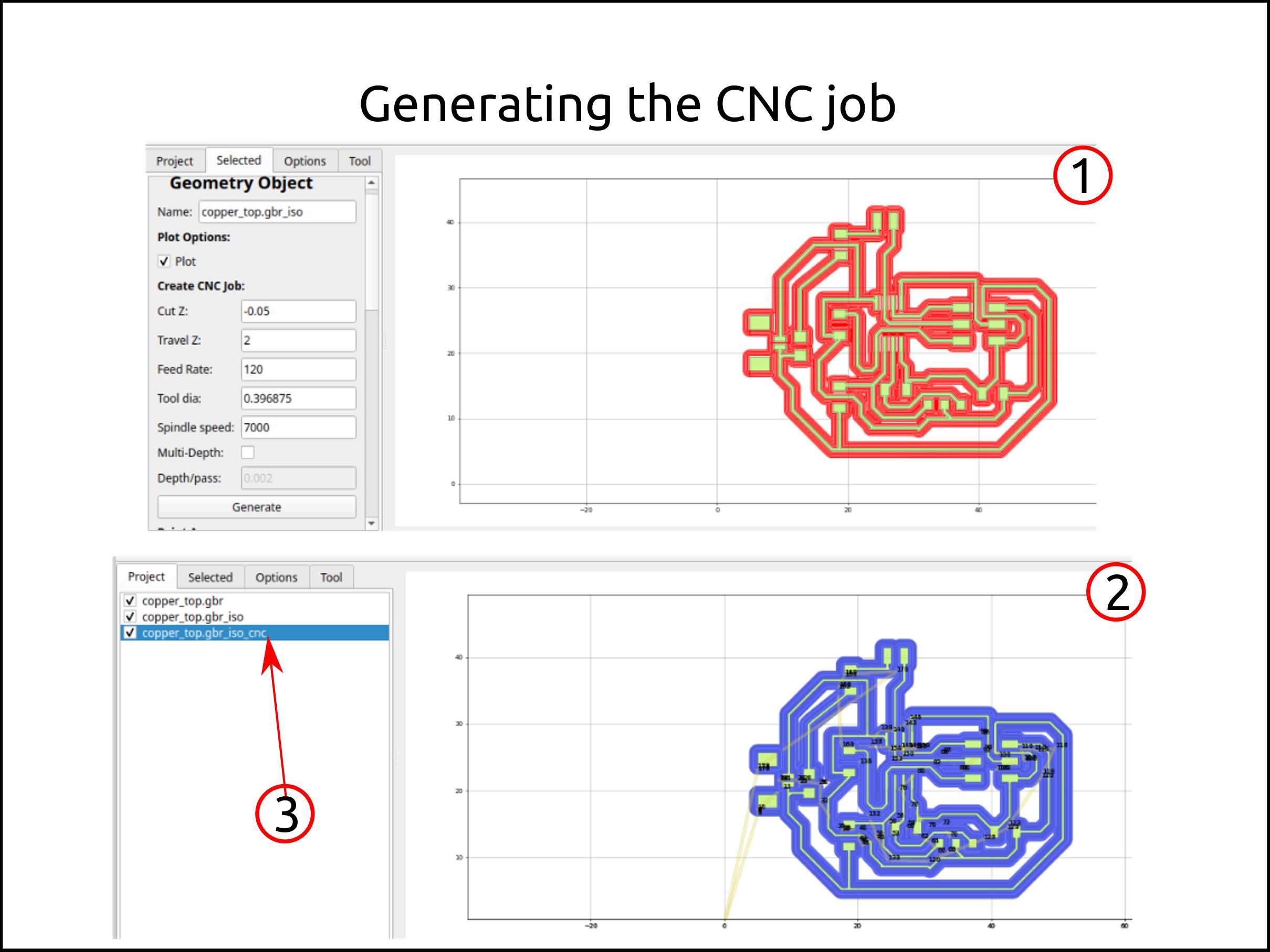
Here I show you the parameters I used for generating the toolpath. The button to press is Generate Geometry.
-
In red will appears the geometry. Here you have to check if the space between traces is enough to pass the end mill between them. You have to see the red generated geometry between every trace.
-
After the toolpath is generated it will appear in the project tab.
-
Doing the double click on the generated geometry you are able to generate the CNC job for the geometry. Here I show you the parameters I used to generate with.
-
The geometry will turn to blue and the is the color of the CNC job.
-
And will appears a new file in the project tab.
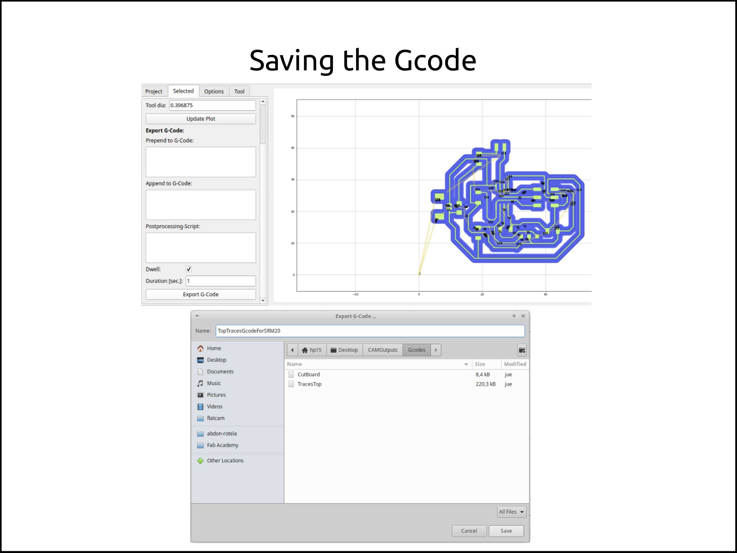
- To save the CNC job to Gcode of your preference you have to double click on the generated CNC job and you are able to choose the extension of your file, choose where you want to save the code set extra codes of Start Gcode and End Gcode. And press save.
-
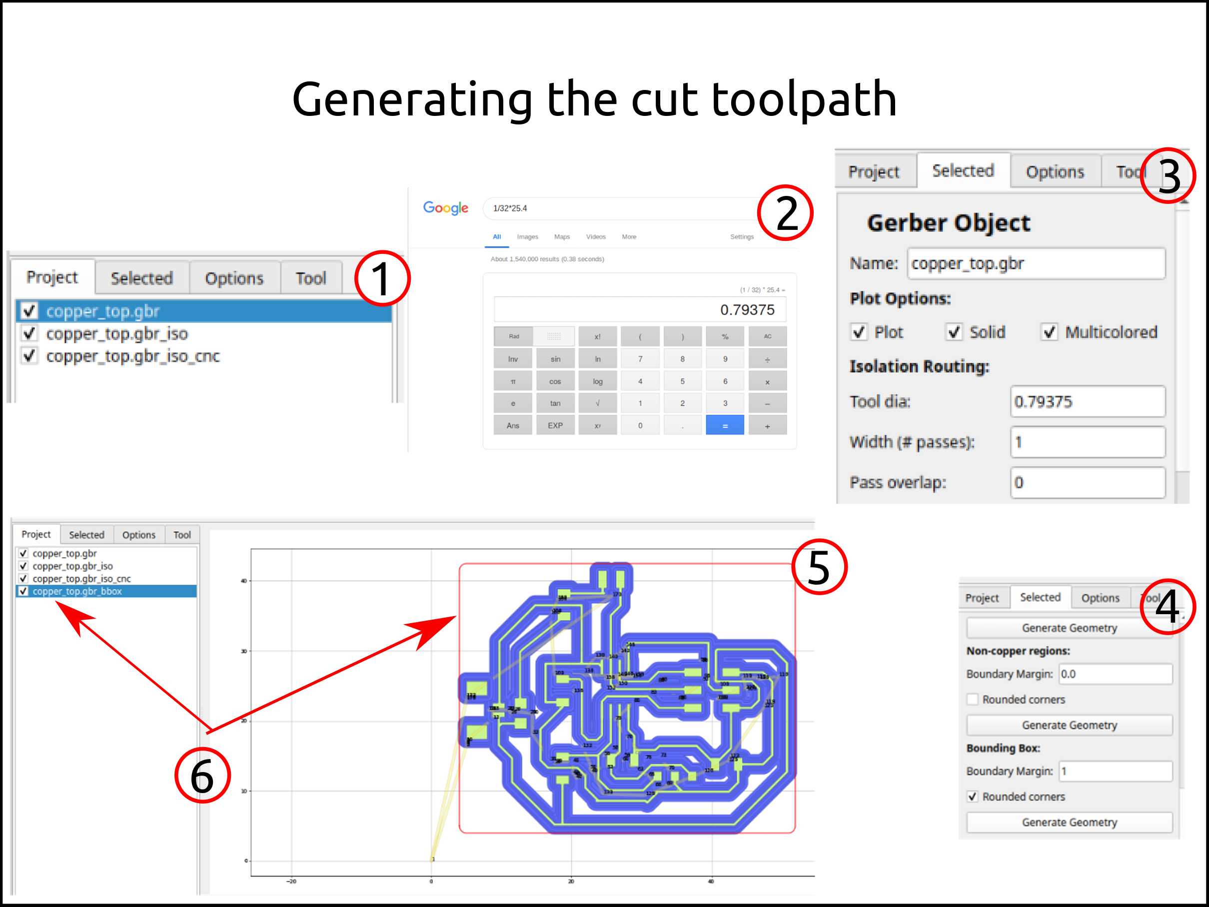
Here we want to generate the geometry to cut the PCB.So, we have to double click the Gerber file you are able to put the parameters for the geometry.
-
Like the first time, I converted the 1/32 in to 0.79375 mm.
-
Set all the new parameters for cutting.
-
In the Bounding Box section, I selected the rounded corner and then the button Generate Geometry.
-
Here you can see the generate geometry that is a bounding box with a rounded corner.
-
In the Project tab, will appears a new file that corresponds to the new generate geometry.
-
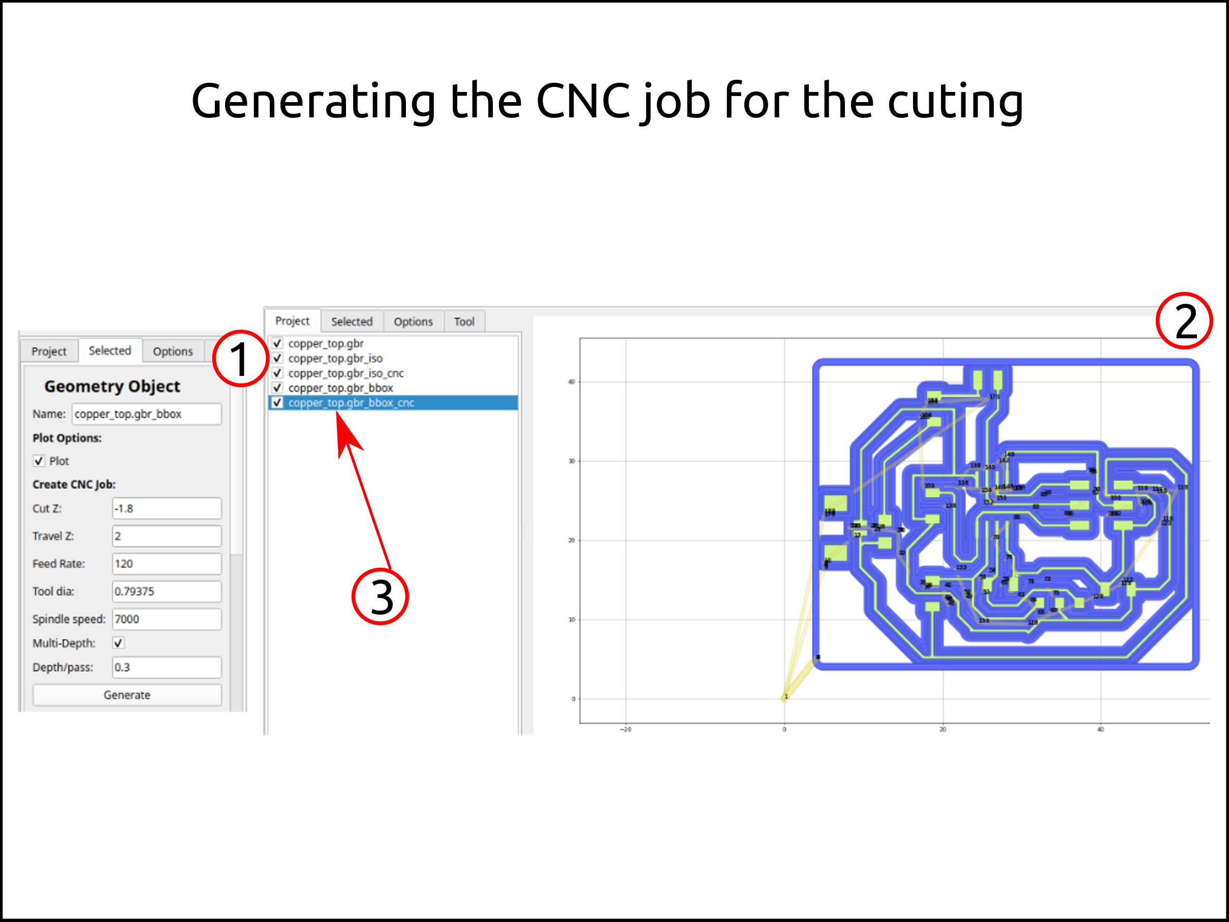
Doing a double click on the new geometry we are able to set the parameters for the CNC job.
-
After setting those parameters and pressing Generate will appears a new CNC job file. All these parameters in the image are the actual parameters I used to cut every board I made using FlatCAM and the Roland SRM-20.
-
The CNC job we will see in blue once we generate it.
-
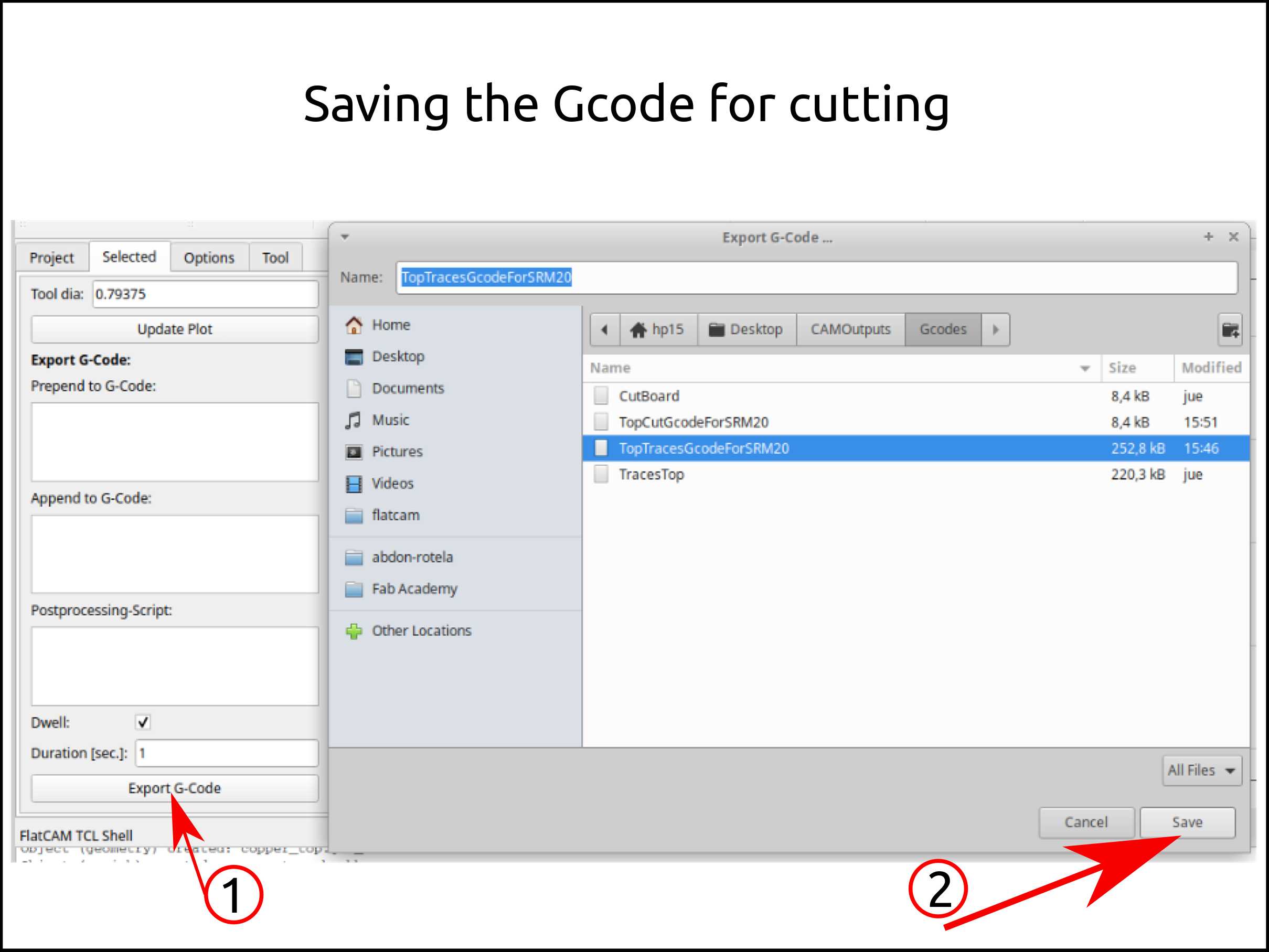
Like the first time, we have to press Export G-Code.
-
Then Save.
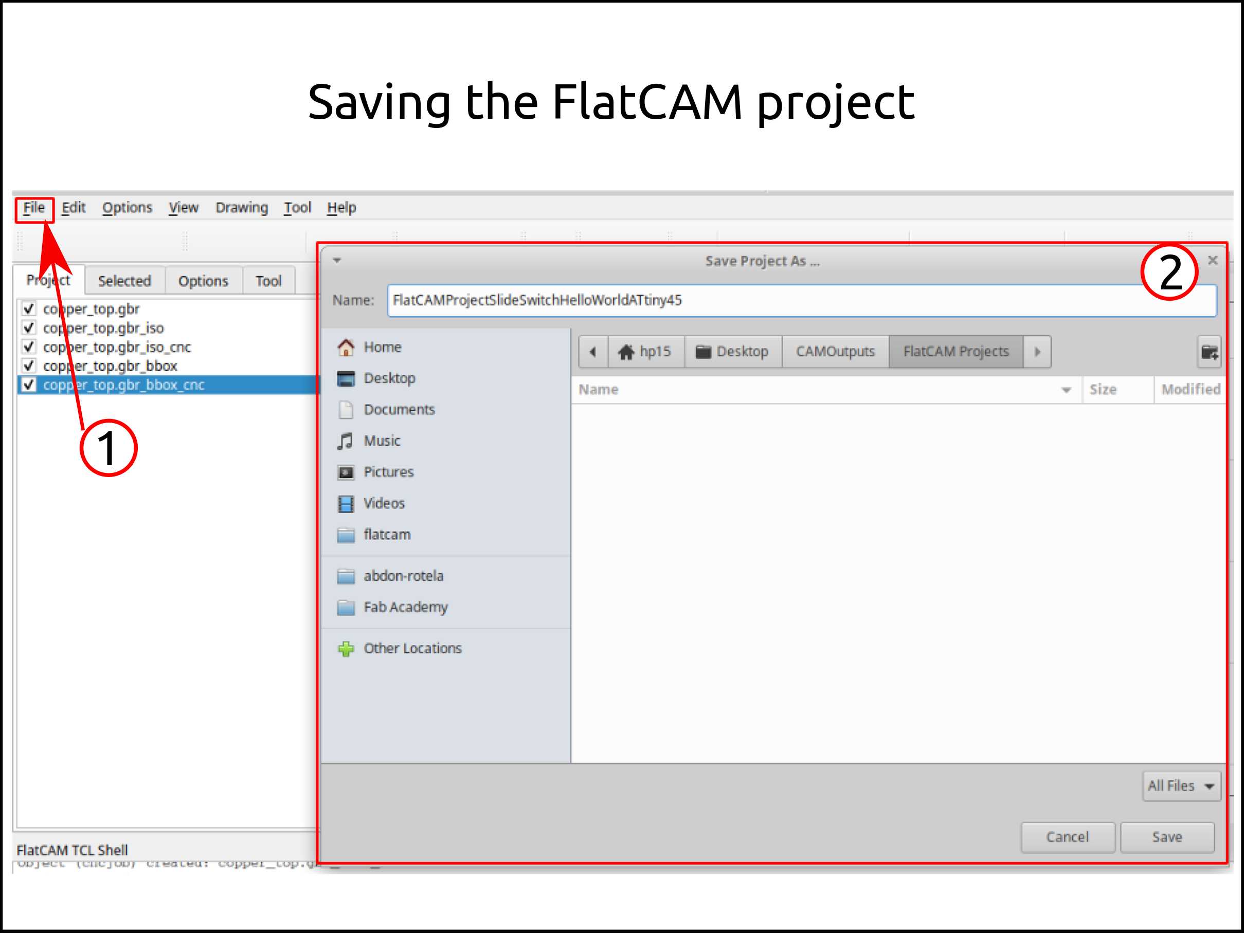
If we want to change something in the Gcode or share it we have to save the project.
-
Go to File/Save Project.
-
Choose the folder you want to save it and press Save.
Faced problems and solutions using FlatCAM
Problems:
-
When I generate traces geometry I choose 4 passes and the software generated for individual geometries and I had to generate 4 individual CNC jobs for each geometry.
-
In the beginning, I could not install the FlatCAM in Linux.
Solution
-
I selected the Combine option and I solve this problem.
-
Meanwhile, I run FlatCAM in windows until I figure how to install it out in Linux.
FlatCAM files
Soldering the components and programming the board
-
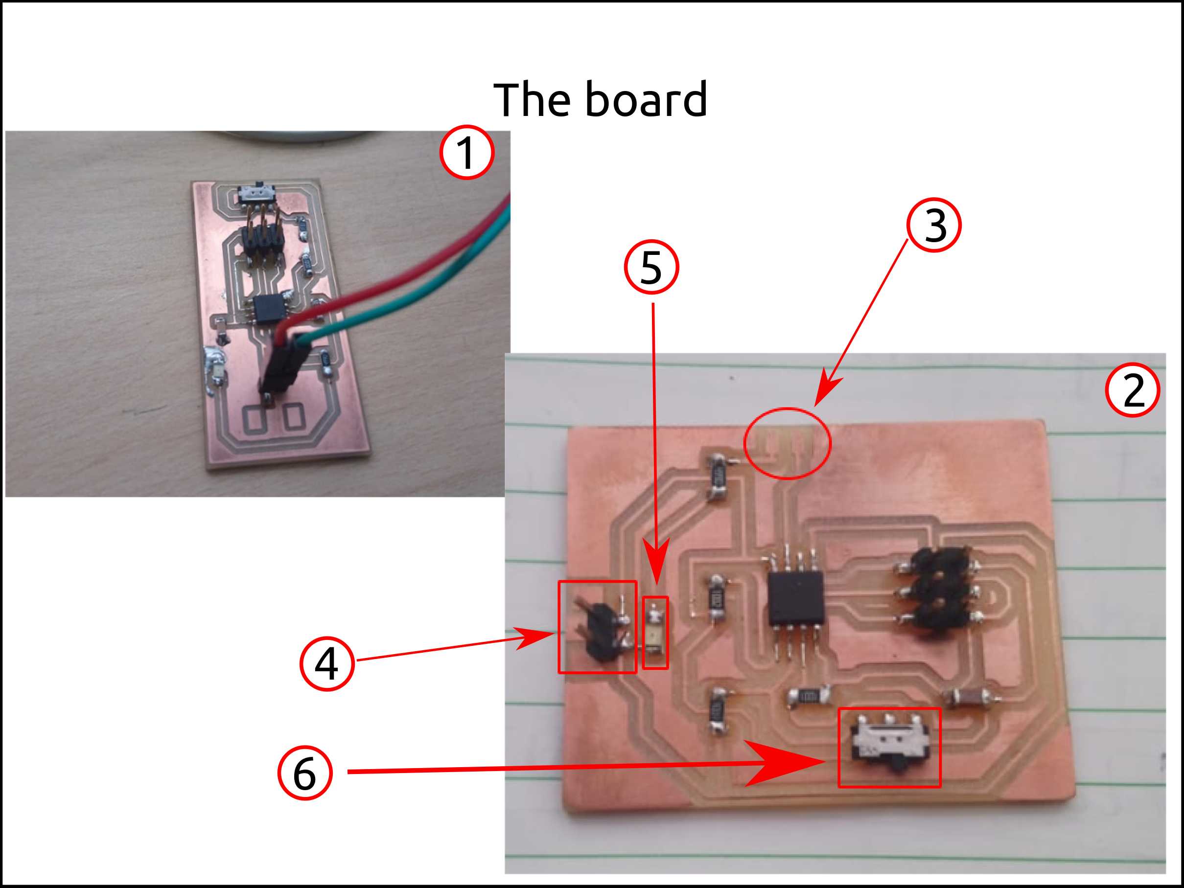
Here I show the boards I made.
-
This was my first design and I could not program it because I connected a load to the SCK pin.
-
This is my second design in which I put a soldered jumper in order to program it before I connect to the SCK pin the load.
-
This is the jumper on the board.
-
This design has two headers for the power supply connection, with it I could energize the board from a USB port.
-
This is the load.
-
This is a slide-switch that I put instead of the button.
Coding and burning the Board
-
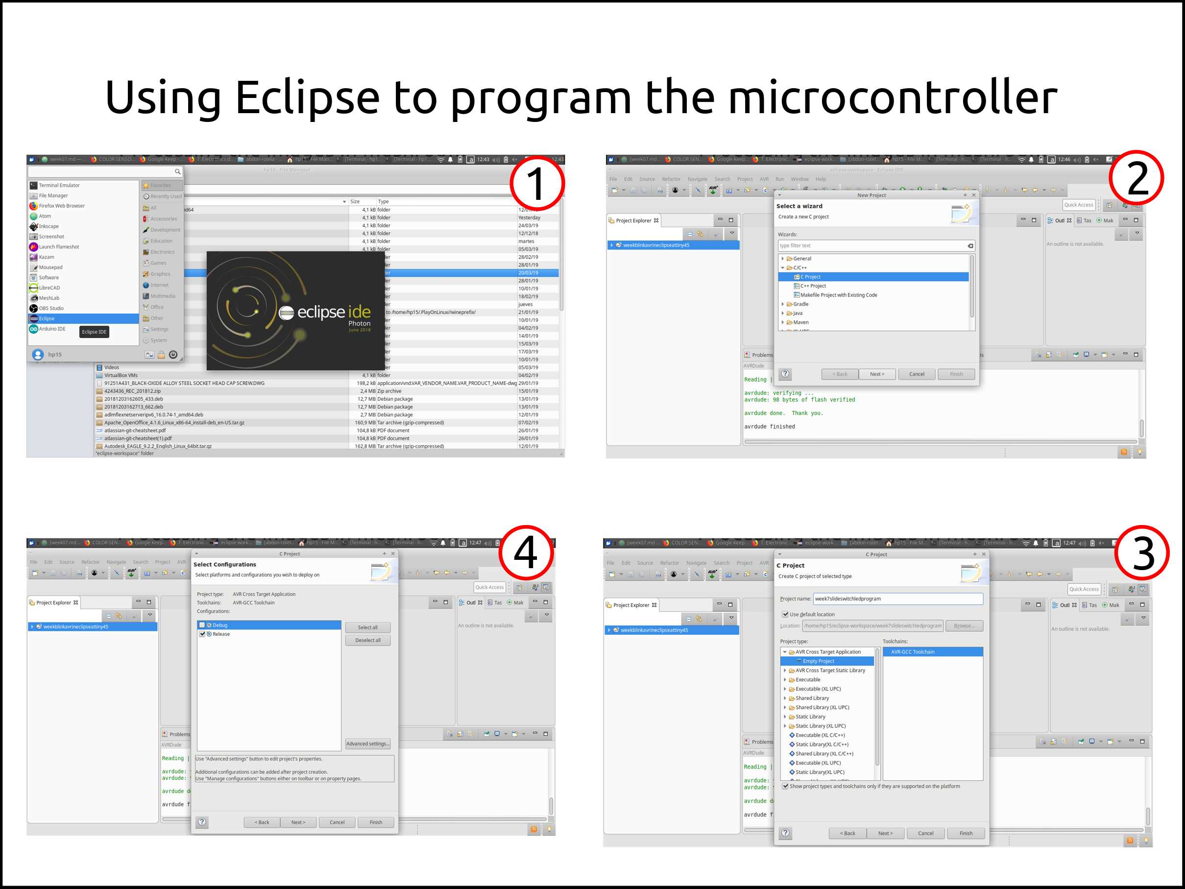
First, we have to open the software Eclipse.
-
Then create a new project.
-
We have to set an empty project with the AVR-GCC Toolchain
-
Select only Release. In this way, we can load to out microcontroller our code. That means it will generate the HEX file. The other option is only for debugging, the same thing as if we are programming with the ATMEL STUDIO in Windows.
-
This is an important configuration in order to compile and burn the chip correctly, AVR Target Hardware properties.
-
Doing right click on the project we make a new source code called main.c.
-
Then we have to type to code.
-
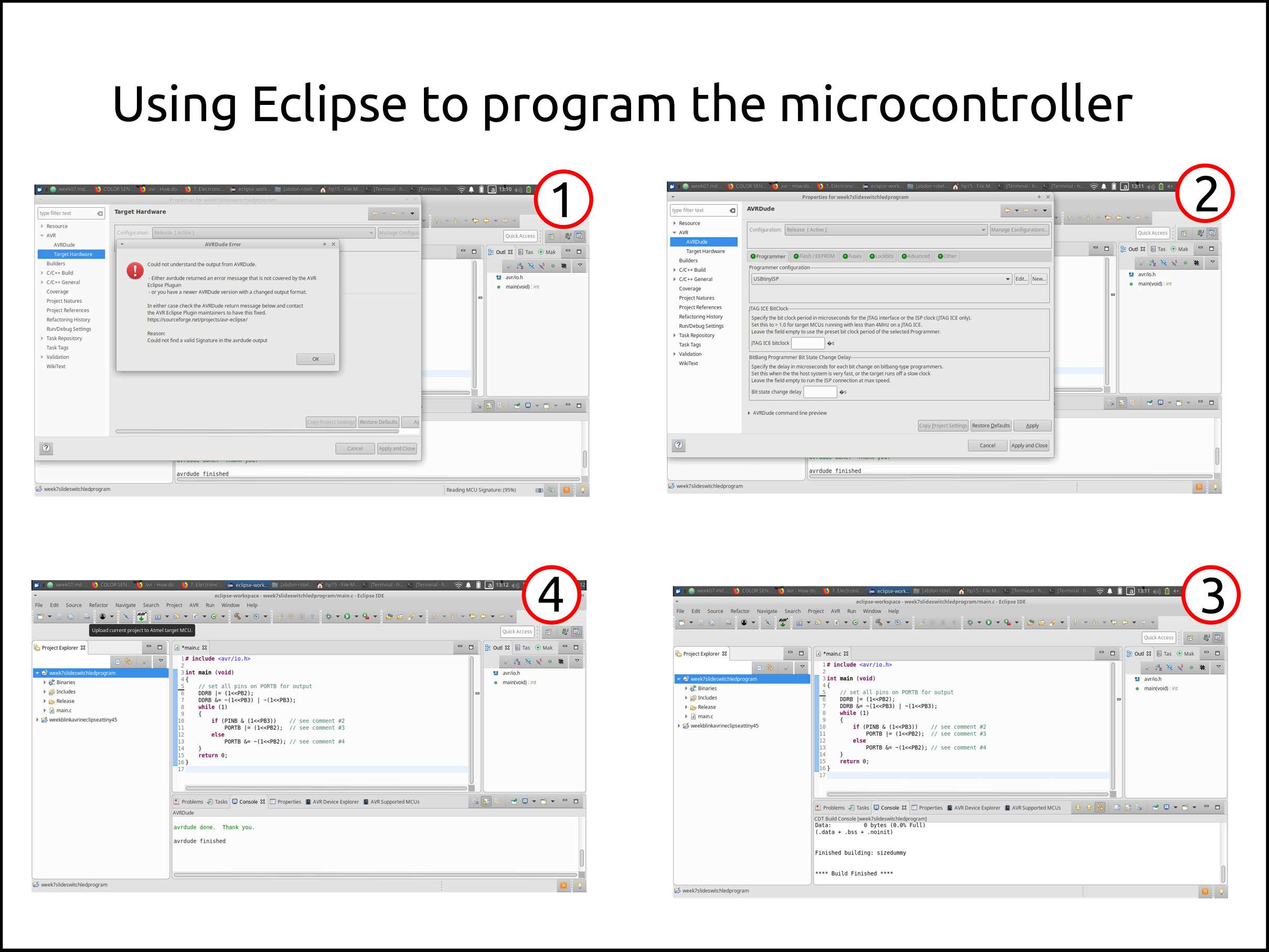
Then right click on the project Properties > AVR > AVRDude and Properties > AVR > Target Hardware
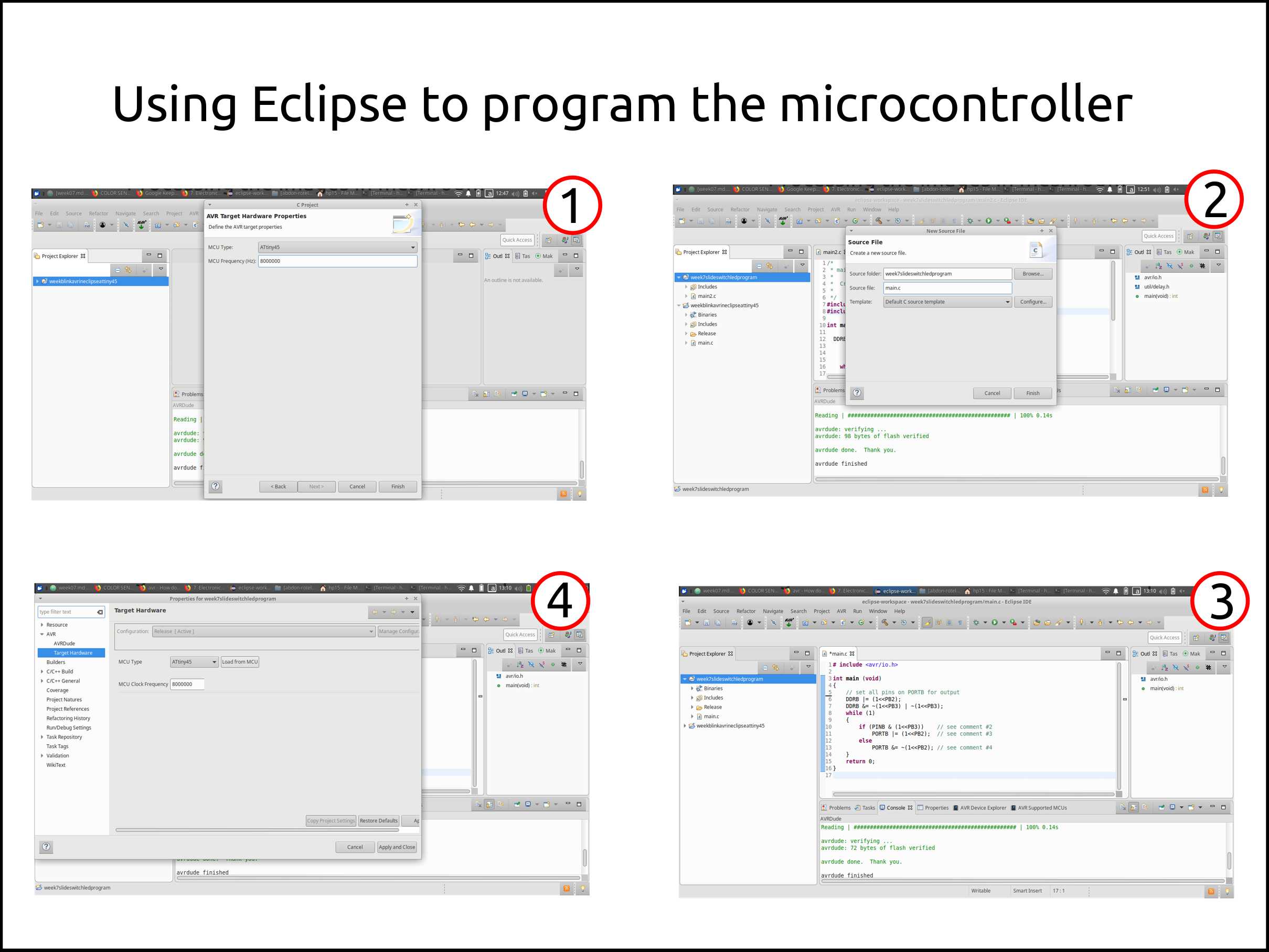
-
This message appears after you select Load CPU.
-
Here we add or select the programmer. In this case, is USBtinyISP.
-
To compile we have to press the hammer and has to appear the message that is in the image.
-
To upload/burn the chip we have to press the button AVR with a green arrow.
File download the project
In this file, you will find the C source code, the HEX file and extra files generated by the IDE software during the compiling process.
Source code
# include <avr/io.h>

int main (void){

    DDRB |= (1<<PB2);               //Sets the PB2 pin as a output
    DDRB &= ~(1<<PB3) | ~(1<<PB4);  //Set the PB3 and PB4 as a inputs
    while (1)
    {
        if (PINB & (1<<PB3))        // Check if the PB3 pin is in HIGH

            PORTB |= (1<<PB2);      // Sets the PB2 in HIGH

        else

            PORTB &= ~(1<<PB2);     //Sets the PB2 in LOW
    }
    return 0;
}
The circuit in action
Faced problems and solutions soldering the components and programming the board
Problems:
- I tried to program my board with my USBTiny with ATtiny45 and I got a signature error.
Solution
- I programmed successfully using the avrisp2 without the signature error. So, I decided to do again for my USBTiny but now using the ATtiny44 version.
What I learned this week?
I learned the AVR Microcontroller Design Considerations.
I learned how to modify the signature of the chip, in case you cannot program it.
I learned that the RST(Reset pin) must have a PULL-UP resistor externally and its value goes between 4.7k to 10K.
I learned that the programming pins have to be load free during programming.