
TARS version 1.0
Electronics

PCBs were designed with Autodesk Eagle. I was preparing for this part from couple weeks. I already worked with ATMega328p. I designed two circuits, which will operate together: Motherboard and Interface. During testing and troubleshooting I managed to finish on versions 1.2, mostly due to ripping traces during testing. Issues will be described in the end.
Motherboard
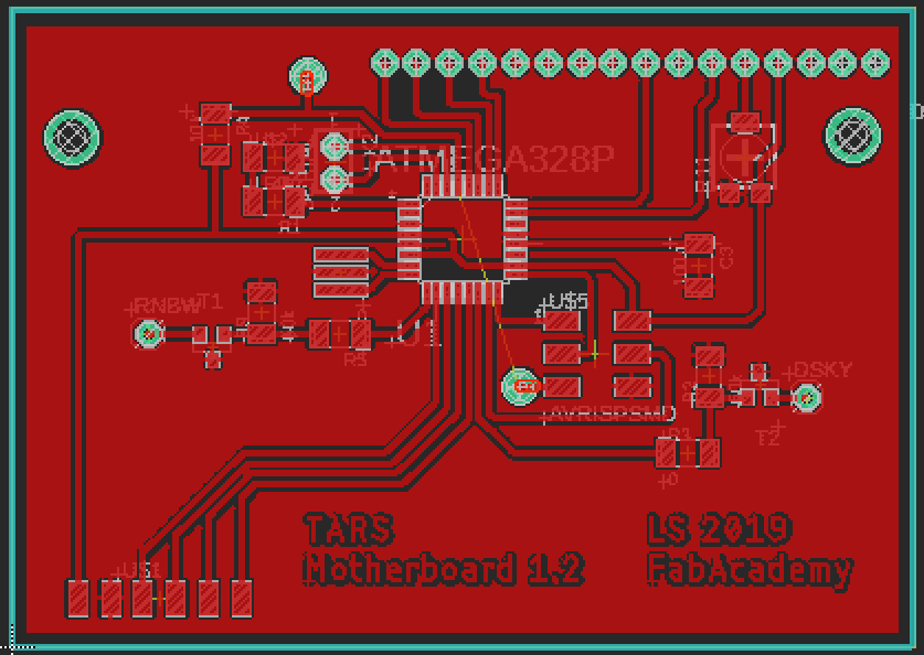
This is a brain of TARS. Central point is ATMEGA328p and from it there are traces going everywhere. Board is 7 x 6 [cm] and it could be easily made smaller. I left it relatively big just for hading purposes. Unfortunately I had to make one connection (ISP - reset pin) using wire as there were no physical way to make this wire on top layer. Let me name features of this board:
- ATMEGA328p - as brain, steering every peripheral
- LCD screen connector with potentiometer - for contrast steering
- 20 MHz Resonator - to speed things up
- ISP - handy way to program it
- Serial port pins - used for testing purposes
- LED (red) - purely testing purposes
- 2 x N MOS transistors - driving High Power LEDs
- FTDI connector - used to connect with Interface board
Below schematic is showing all of the features included on Motherboard 1.2.
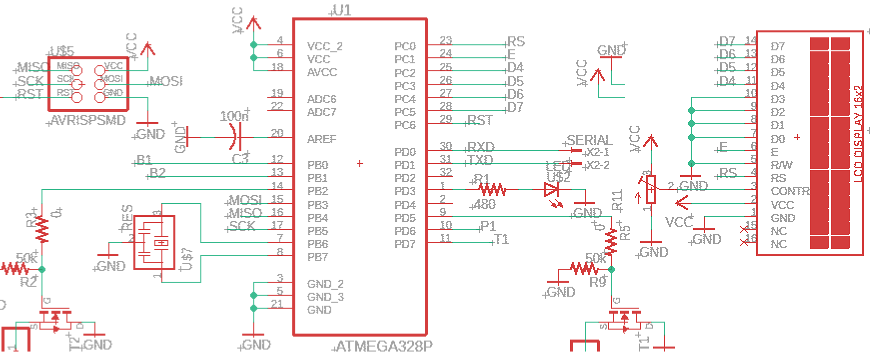
After some time spend on it I was quite happy with printer circuit board. As I was mentioning before straight and nice lines makes me happy. Yellow line (airwire) is connection between ATMega's and ISP reset pins.
Interface
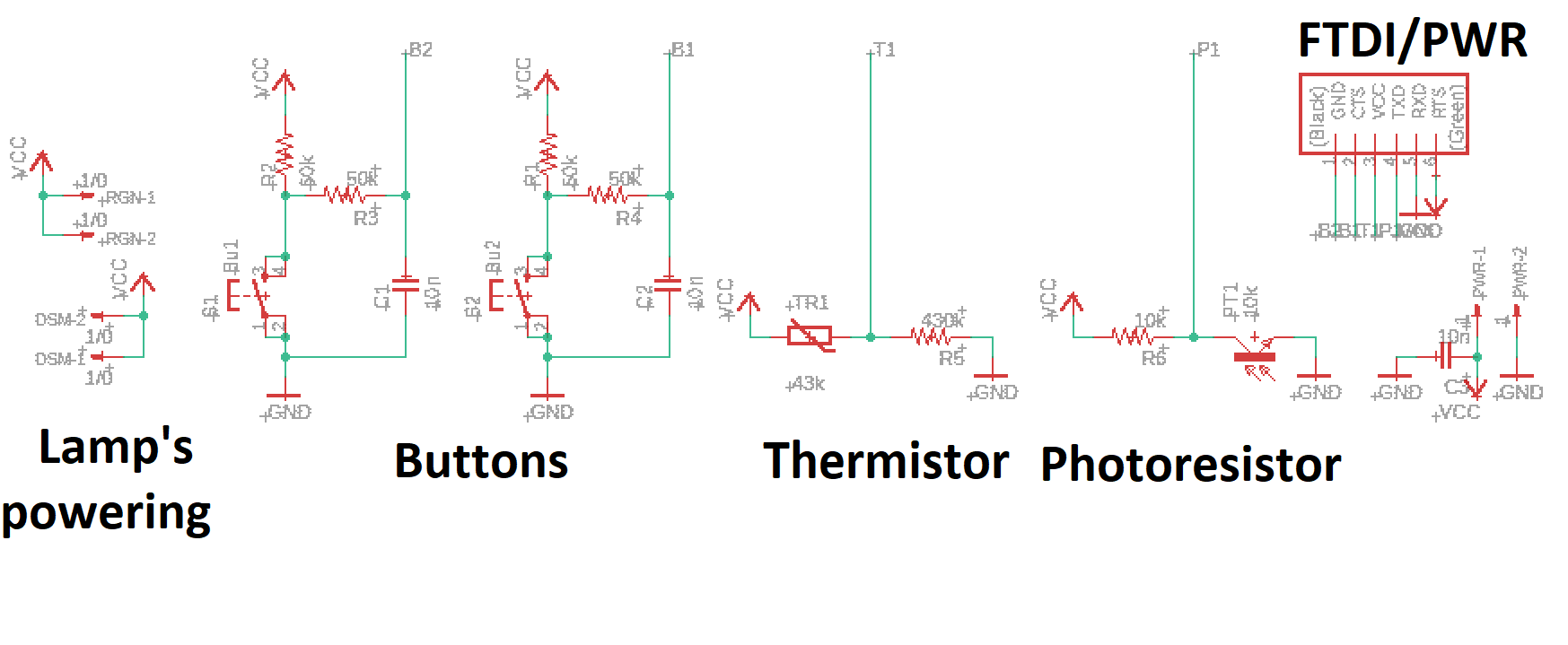
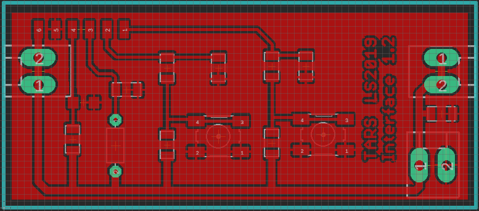
I value second board, which I called an Interface same high as motherboard. In general it is a powering unit with additional connectors for inputs and outputs. PCB is a bit smaller than Motherboard and falls within 7 x 3 [cm]. I ended up with version 1.2 as well. There were no major issues. Nevertheless, I moved some parts.
- Phototransistor's - voltage divider with wire connection pads
- Thermistor circuit - voltage divider with wire connection pads
- 2 x Buttons - with debouncer circuits
- Power connections - to distribute power to HP LEDs
- FTDI connector - used to connect with Motherboard
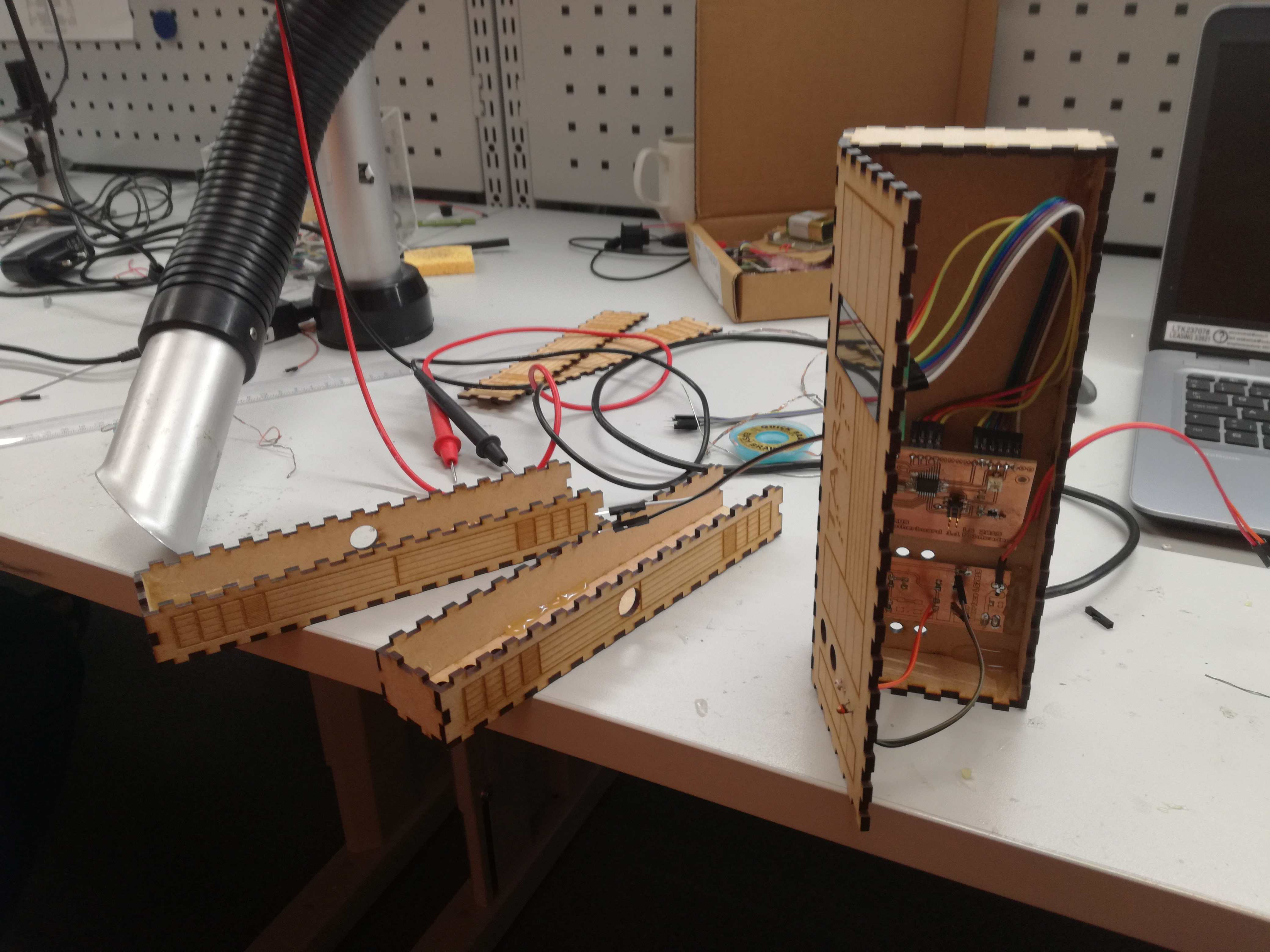
High Power LED circuit
There are no fireworks (gladly) in here. There was no need for anything else than STAR LED soldered together with 12 Ohm resistor.Together there were placed on radiator and thermal paste for better connection and heat exchange. Embedding them inside of the arms is shown below. Those were later raised in order to minimize optical power losses.

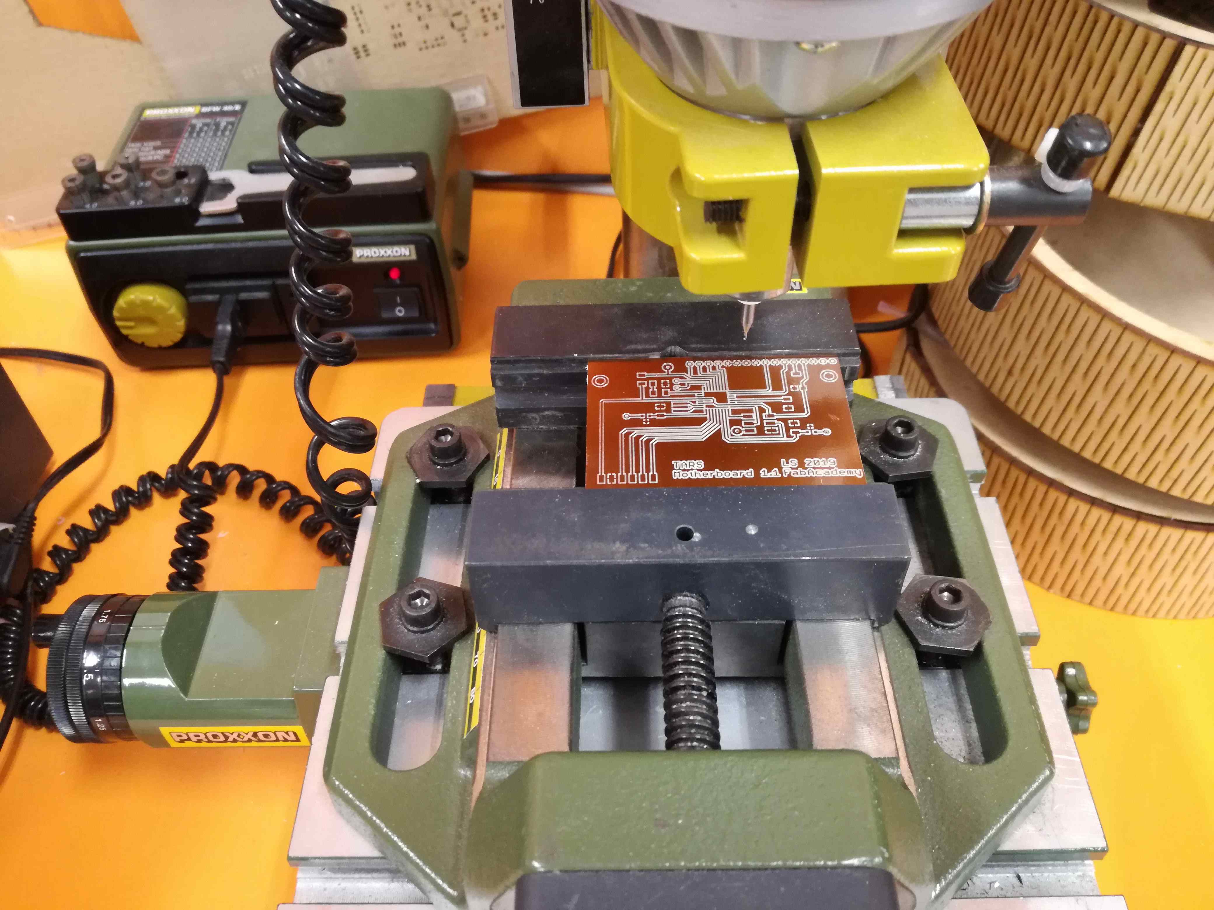
Milling
Traditional approach to milling. First I exported PCBs as images and then used mods. Sidenote: As I used clearance of 16 mils and same width of wires in MODs I changed size of the milling bit to 0.25. Later I used a milling bit with even smaller size but whole point is to create clearances between ATMega328 pins. Below couple images from the process of creating Electronics.


Hero shot
I was well prepared for making Electronics. Most of the job was already tested or done during following:
Troubleshooting and conclusions
With electronics there is always plenty of things, which may go wrong. This is why I started preparations quite long time ago and tested everything beforehand. Pin maps are extremely handy when programming with ARDUINO IDE. Moreover, good planning is a key. There is plenty of signals and some of them might be put on the printed circuits rather than be hanging wires. There are always limitations space. If elements are PCB board can be quite small. Regarding components, it is important to read datasheets. Transistors, LCD screens and especially microcontrollers will work much better when you are understanding those parts.