11. Input devices
Individual Assignment
Board Design
I want to use the current and next week to design the electronics which I can use in my final project. So, I decided to make a breakout board for ATmega16U2 with a micro USB connector, as I want to use this microcontroller in my final project.
The design was straightforward with an ATmega16U2 connected to the basic required components and rest all of the available pins exported to jumpers.

|
|
| |
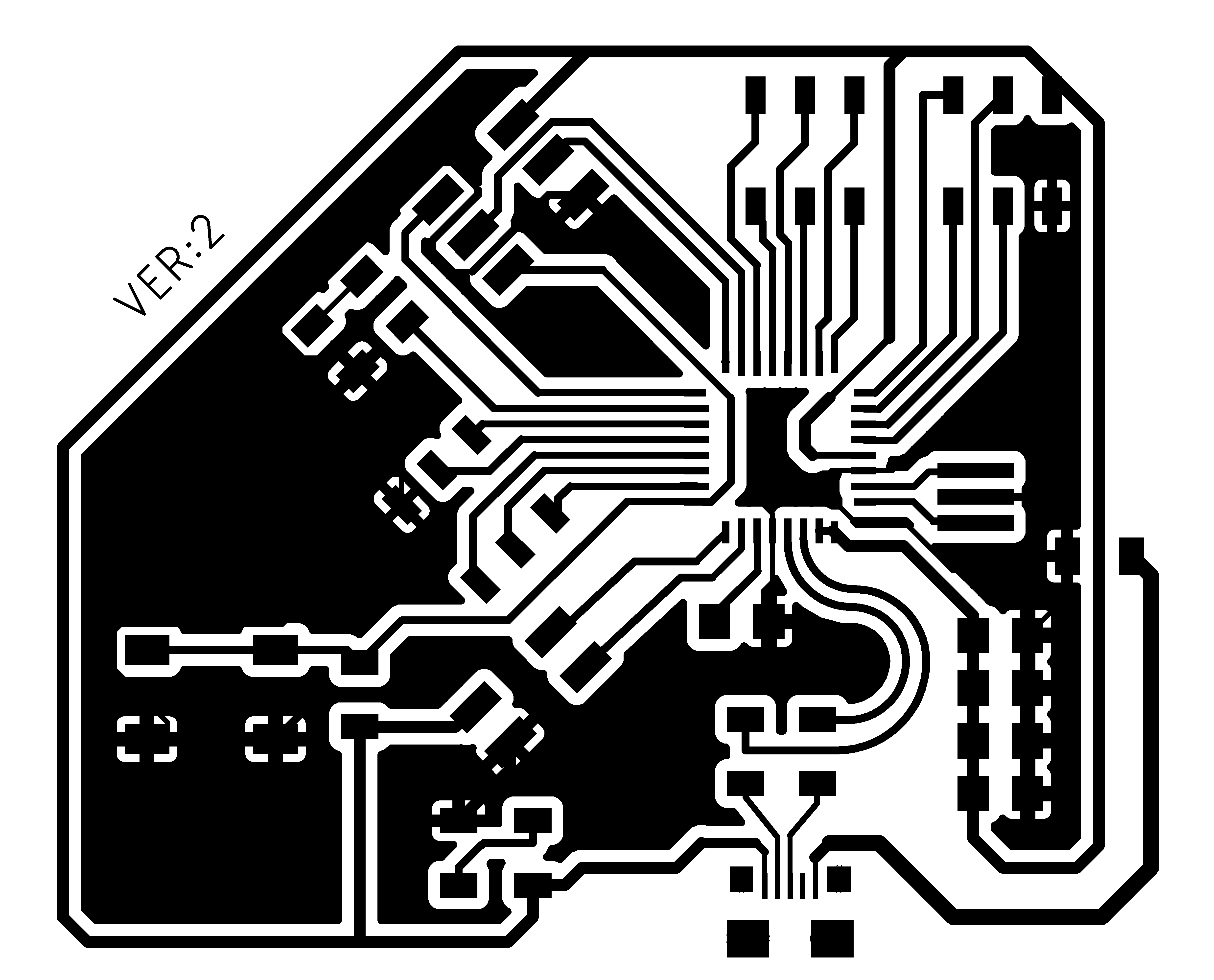
Given the small pitch of the ATmega16U2, I ended up using lot of 10mil traces, furthermore lot of traces were not very far away from each other, which meant I had lot of DRC errors when I ran the DRC on the finished PCB. It was fine though because I was planning to use 0.2 mm V shaped end mill instead of the flat 0.4mm end mill and the DRC rules were defined for the flat end mill. However, look at the blue circle part of the image and these two traces ended up merging with each other. While inspecting the mill path I found that there were no tool paths defined in that area, so the take away is that you can have DRC errors but you should very carefully inspect the tool paths before milling.

|
In the first version of my ATmega16U2 breakout board, I had vdd trace going under the microUSB connector. When I soldered it, everything was fine till I inserted the USB cable. As I didn’t properly reinforced the connector, the connector insertion force was enough to rip the connector of the PCB and it took the traces too. For the next two hours then I did multiple micro surgeries on the board and every time after reinforcing the connector, I managed to short the vdd with ground. This went on till I managed to lift the big ground pad underneath the connector.

|
Well, time to design another version with fixes. Below are the major changes
- No trace under the micro USB connector
- Thicker traces
- More distance between traces

|
I managed to finish the board manufacturing in next week only, so further updates regarding this board is under week 12 page.
Reflections
I managed to fix the board. There were problems with both software and hardware. All the details can be found from the Output Devices page. Based on my experience with the board bring up, I can define following guidelines
- On a single layer board, do not put any trace under the micro USB connector
- Do solder the body of the connector with the ground plane of the board
- Properly select the resonator or crystal. USB device will work only with few selected combinations
- Reset pull up resistor is essential while stuffing
- While generating the tool paths, make sure that the tool is going at all the places where there are different traces (check the marked area in the image of the first version of the PCB)
Sensors
I wanted to use the distance sensor, however FabLab Oulu does not have the HC-SR04 (ultrasonic sensor module) in inventory and I had no plan of making the analog receiver and transmitter myself, so that plan is out of the window. The next bet is to use the Hall sensor, so I made the breakout board for the Hall sensor.
Update: Found a HC-SR04, will play with it and update the page when I have any new things to report.

|
|

|

|
Embedded Software
Unfortunately ATmega16U2 does not have an ADC inbuilt into it, so in order to digitize the analog data from the Hall sensor, I used the ATtiny44A board that I had designed during the week 7. I soldered female pin headers to pin number 10 (PA3) and connected that to the Hall sensor analog output.

|
|
I modified Niel’s Hall sensor code to work with my board. The changes were related to the different pin and different ADC registers. In the below code snippet, I have changed the serial pin that is used for transmitting the data.
#define serial_port PORTA
#define serial_direction DDRA
#define serial_pin_out (1 << PA1)
Below are the changes related to ADC registers in ATtiny44A. Mentioned below is the functionality of the used registers according to the datasheet
- ADMUX: This registers selects the reference voltage and governs which analog input is connected to the ADC.

ADMUX register. - ADCSRA: It is the first ADC control and status registers

ADCSRA register. - ADCSRB: It is the second ADC control and status registers

ADCSRB register.
    ADMUX = (0 << REFS1) | (0 << REFS0) // Vcc ref
    | (0 << MUX5) | (0 << MUX4) | (0 << MUX3) | (0 << MUX2) | (1 << MUX1) | (1 << MUX0); // , PA3
    ADCSRA = (1 << ADEN) // enable
    | (1 << ADPS2) | (1 << ADPS1) | (1 << ADPS0); // prescaler /128
    ADCSRB =  (0 << ADLAR); // right adjust
For the visualization, I again modified Niel’s code. The original code was designed for Python 2.7, so I modified it a bit to run with Python 3.4. Below is a short video showing the visualization along with the sensor.
Group Work
We (Michael, Jobin, Sahan, and Yasir)tested the hall sensor board by directly powering it up from a power supply and measuring the output voltages.

|

|

|
When we brought south pole of a strong magnet, the output voltage shot up to 4.97 V and when we flipped the magnet the voltage dropped to almost 0 V, thus confirming that the sensor is working. The procedure in software to convert this analog signal into digital is exactly the same as mentioned in the Embedded Software section above. As the digital signal is being put on the FTDI bus as a serial data, it is going to look exactly the same as a serial signal. Images of how a serial signal looks on an oscilloscope can be seen on week07 assignment.
Details of connecting the signal from Hall sensor to the oscilloscope and visualizing it there can be seen from Michael’s page.