Assignment
group assignment:
characterize the design rules for your PCB production process
individual assignment:
make an in-circuit programmer by milling the PCB,
program it, then optionally try other PCB processes
characterize the design rules for your PCB production process
The machine used: Roland MDX-40
The idea is to understand the different settings of the CNC milling process that could affect the output products. There are many variables in the Milling process setting that could be changed and respectively affect the output of the machine. The settings are:
- RPM of Milling Bit is the variable that controls the rotating speed of the milling bit.
- Mrilling Bit Diameter is the variable that is directly related to the bit diameter. The bigger the diameter, the less we can achieve thin connecting lines.
- Feed Rate is the variable that controls the rate the milling bit moves on the surface of the copper board. Milling the inner lines requires a normal feed rate. However, milling the outer parameter of the pcb required very slow feed rate.
- Offset Number is the variable that controls the number of passes the milling bit does over the same path. This setting majorly affects the final product. Paths that are not cut in the first pass most probably will be cut during the other passes.
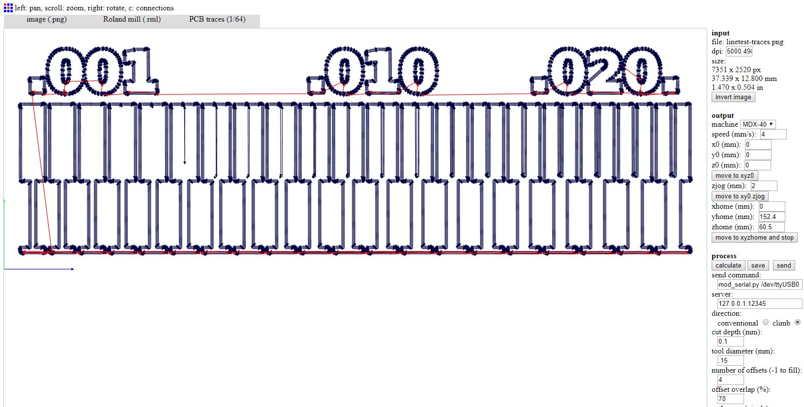
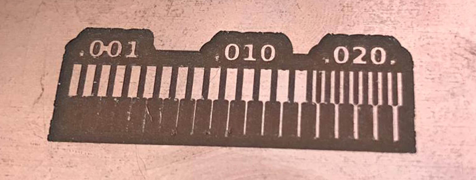
We started by a Test File we got from the internet, that has different paths of various thicknesses. We tested milling this image using the milling bit of diameter 0.15mm.
The test file was downloaded from the following Link
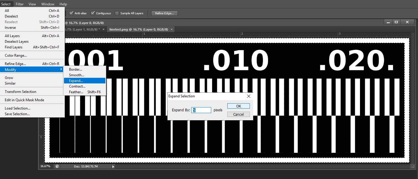
Before milling the test file we had to create 2 images, one for the internal traces and one for the outline cutout.For that we did the following:
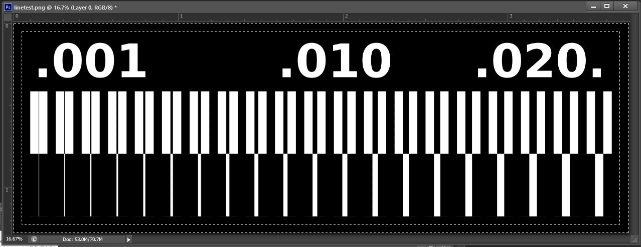
- Open the file in Photoshop, and select the white border by the magic wand tool then go to select /expand and hit 5 pixels.Then use the brush tool to paint the selection in black. We did this to make sure that the selection is bigger than the white border and there is no gap between the new black and the old black in the center.
- Now we will save it as the Inernal Traces.
- We open the original file (the one that was downloaded) and select the white border , paint it in black then we select inverse to select the other part and paint it in white making sure there is no black part left.
- Now we will save it as the Outline Cutout.
Now we will calculate the g-code for these images

The results:
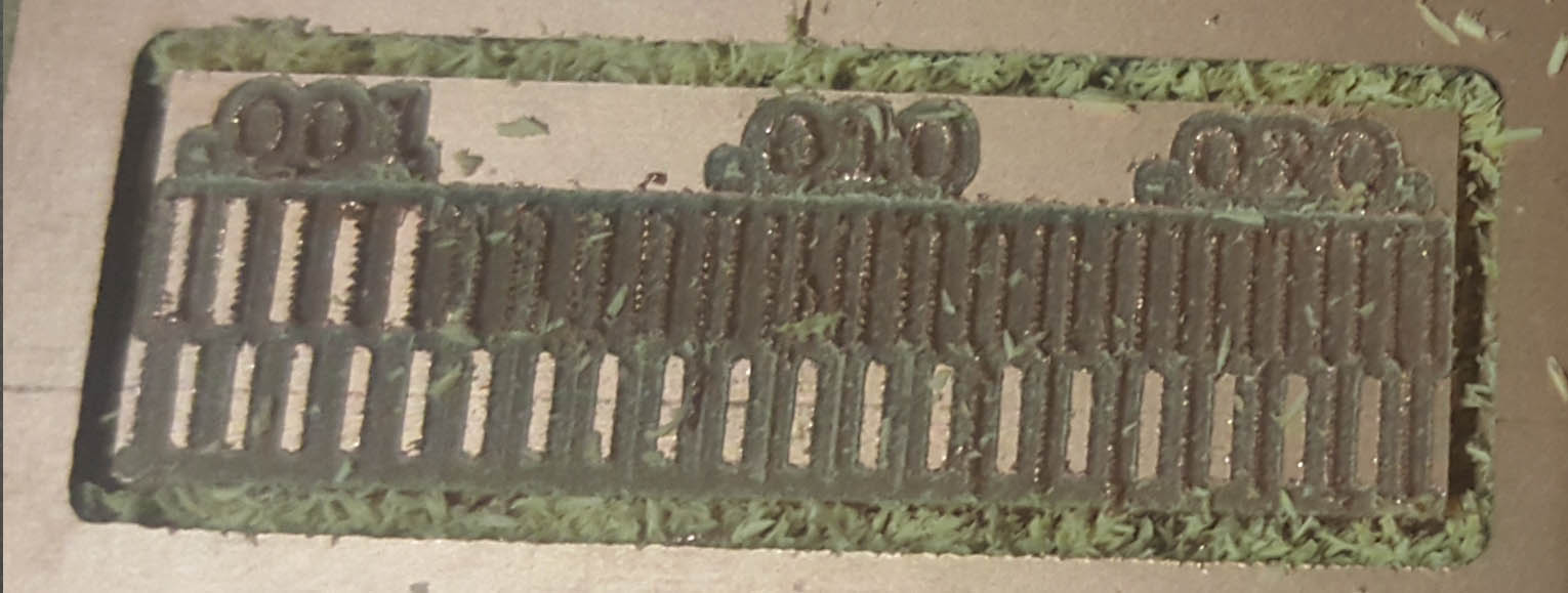
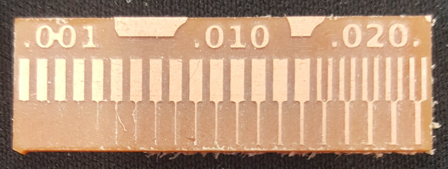
The result are not very satisfying, so we decided to do another test with another milling bit diameter 0.4mm instead of 0.15mm
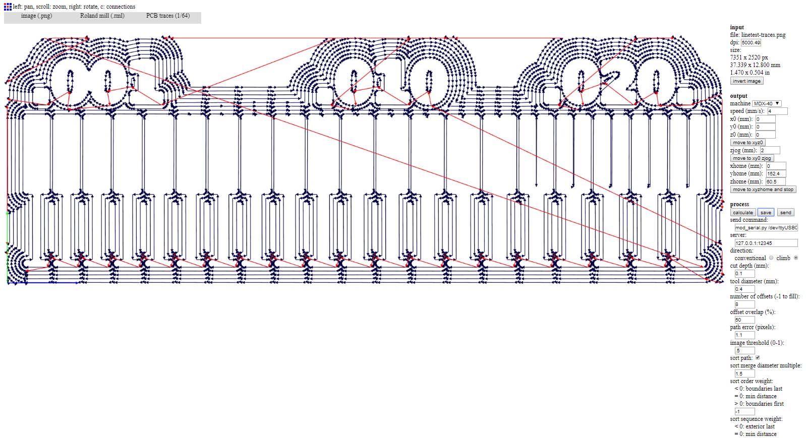
The new g-code:
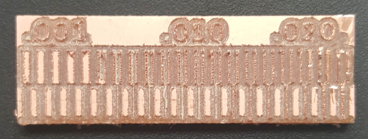
The new results:
make an in-circuit programmer by milling the PCB, program it, then optionally try other PCB processes
To build our own ISP(In-system programming) we need the following:
- Preparing the Design
- Extracting the PCB Layout Image
- Producing the G-Code
- CNC Milling the PCB Board
- Welding the Components
- Programming the Microcontroller
1-Preparing the Design
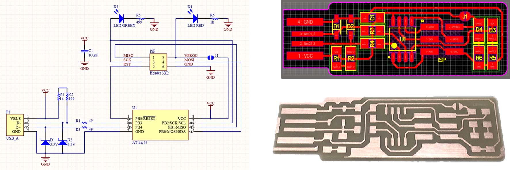
We had different design to choose from , I have decided to use the BRIAN pcb.
The schematic diagram and the PCB layouts are usually done on Eagle software.
2-Extracting the PCB Layout Image
After finalizing the design on Eagle, the next step is to extract the final layout of the PCB, which mainly represents the location of the different components and the connecting lines between them. The image should be extracted from Eagle in a Monochrome setting, and opened in GIMP or Photoshop to enhance the extracted layout and produce 2 different images:
- Image 1 that represents the internal traces of the PCB
- Image 2 that represents the outline cutout of the PCB
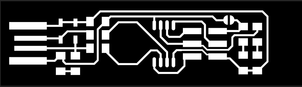
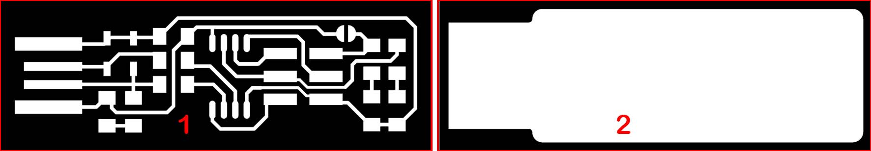 In my case I download the BRIAN images for the traces and the board outline cutout:
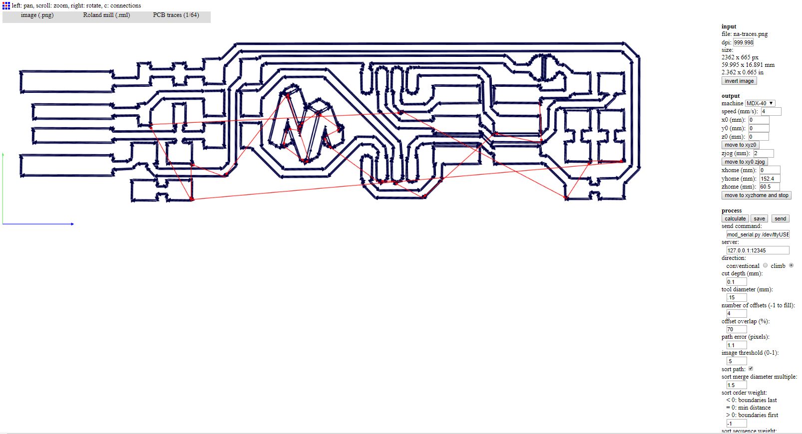
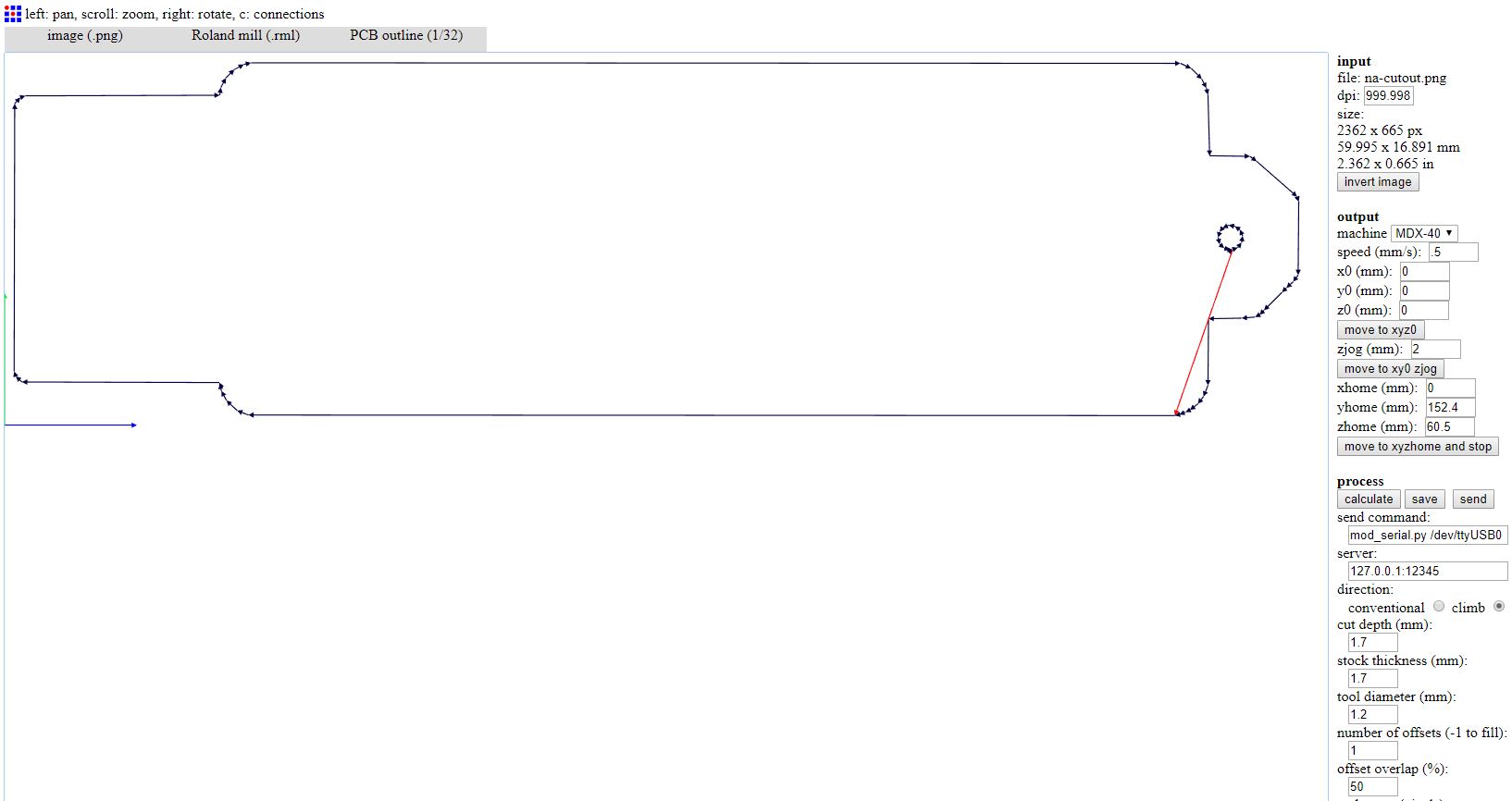
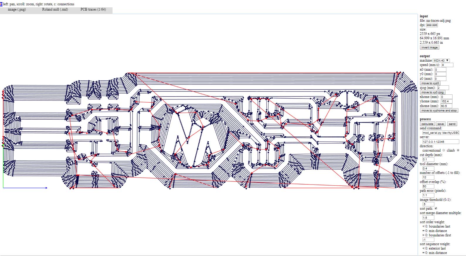
3-Producing the G-Code
I will use Fab Modules to produce the g-code for PCB milling on the ROLAND MDX-40.
Below are the steps followed on Fab Modules to generate the g-code:
- Choose input format and select image (png) that the g-code is going to be generated from
- Then select the file from the specific folder
- Then go on to Output format and select the format that applies to the CNC machine you are using, in our case it was Roland mill (.rml)
- Then select Process and choose PCB traces (1/64) for internal paths and PCB Outline (1/32) for the external cutting.
- Then under Output, select the CNC machine you are using, it was a Roland MDX-40. Under speed 4mm/sec for the Internal Traces and 0.5mm/sec to the External Cutout. Change the X0, Y0 and Z0 to save space on copper board used.
- Then Under Process, adjust the cut depth which should be 0.1 mm for the internal tracing, and 1.7mm for the external parameter. The tool diameter (milling bit) which was 0.15 mm for the Internal Traces, and 1 mm for the external Cutout.
The Number of offsets is 4 and the offset overlap used is 70%
No other adjustments need to be made. - Once the Input, Output, and Process tabs have been adjusted and double checked. Go ahead and press the Calculate button
- Then finally click the Save button and save it to the designated folder. It would be saved as an .rml file
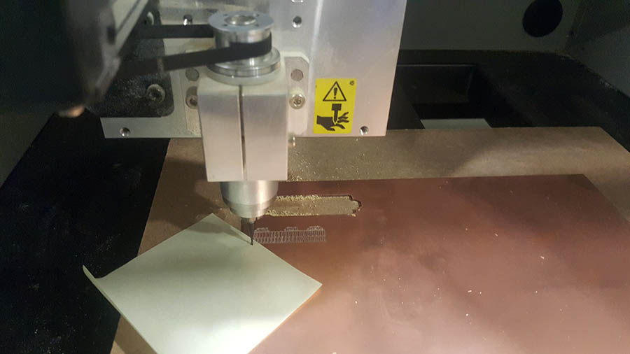
4-CNC Milling the PCB Board
After preparing the G-code, the following steps were taken to mill the layout onto the copper board:
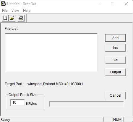
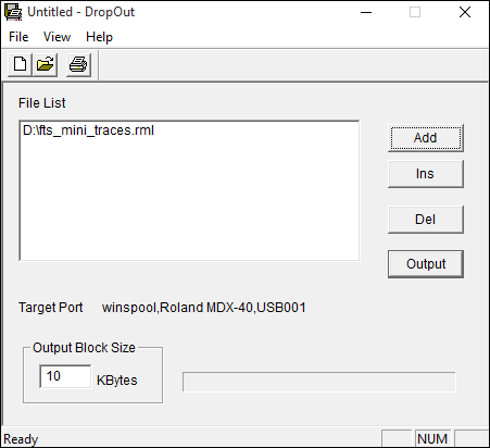
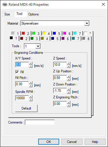
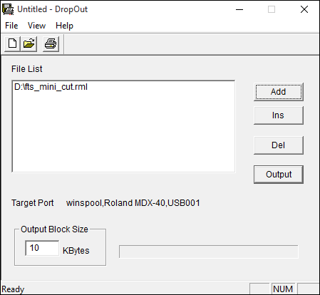
- First I needed a software that would send the g-code directly to the Roland MDX-40. In my case I used the Drop-Out software to send the .rml file to the CNC machine
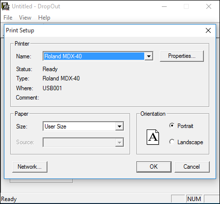
- Then go to File and select Print Setup
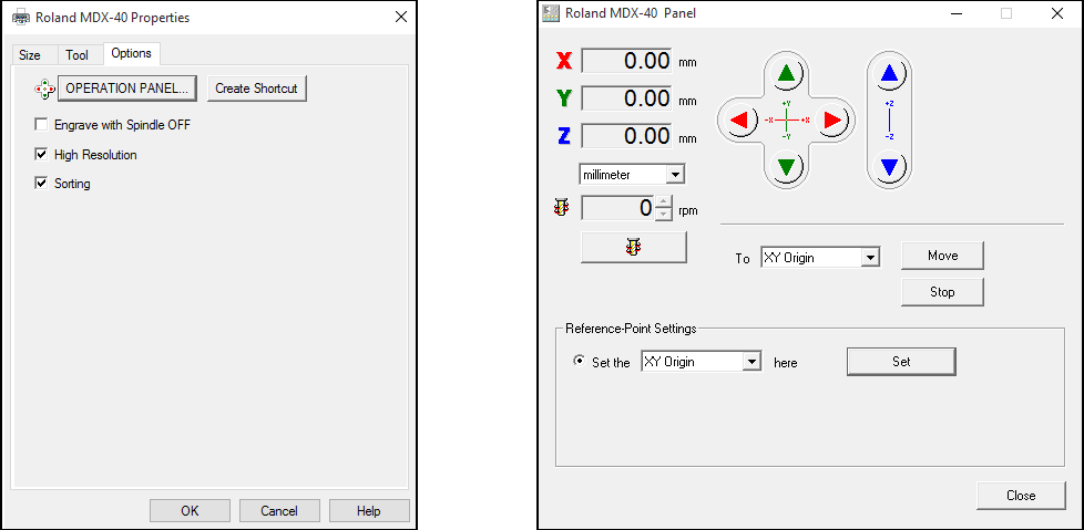
- On the Print setup first choose the name of your printer, in my case it was the Roland mdx-40
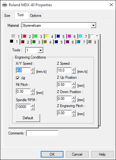
- Then go to Properties and press the Tool tab, the only thing that should be adjusted are the Z Down Position and Z Engraving Pitch both should be at 0.00 mm. The X/Y Speed should be 4 mm/s and the Spindle RPM should be 10000.
- Then go on to the Options tab and select Operation Panel
- Set the X and Y-axis on the position where you want your PCB to be engraved on the copper board inside the CNC, then press the XY origin SET button
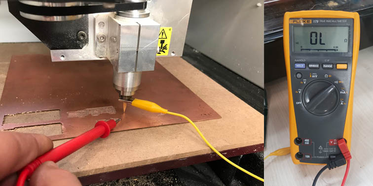
- As for the Z-axis, we needed to zero the tool at the top surface of the copper board. In order to do this delicate process we need to gradually bring it down onto the board, with the help of a multimeter with the beep mode on and have one of the cables on the copper board and the other on the drilling bit. In this case as soon as the drill-bit touches the copper board the multimeter would beep. Make sure to go extremely slow at the end so you don't risk breaking your drill-bit
- Once the beep is heard, you know that the drilling bit is right at the surface and you can go back to the operational panel (on Drop-out), and the Z axis is set automatically to zero.
- On the Drop-Out application press the add button and choose the .rml file you created and press open
- Once everything is set press the Output button. Your CNC machine should now start the process of milling/engraving the copper plate set inside. watch the process until its done
- I will repeat the same steps for the file of the external cutout, after changing the drilling bit to 1 mm. I should not change the X and Y axis. I just need to reset the Z axis. I don't need to use the electrical tester in this case, I will place a paper under your drilling bit and keep pushing the Z axis down until the paper is not coming out very easily from under the drilling bit
- Then go again to Properties and press the Tool tab, the only thing that should be adjusted are the Z Down Position to -1.7 and keep Z Engraving Pitch at 0.00 mm. The X/Y Speed should be 0.5 mm/s and the Spindle RPM should be 10000.
- On the Drop-Out application delete the older .rml file and add the cutout .rml and then press the Output button.
- Check the final result, using a multimeter with the beep setting to make sure components are isolated and all conductivity channels are connected
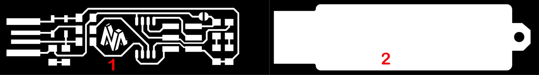
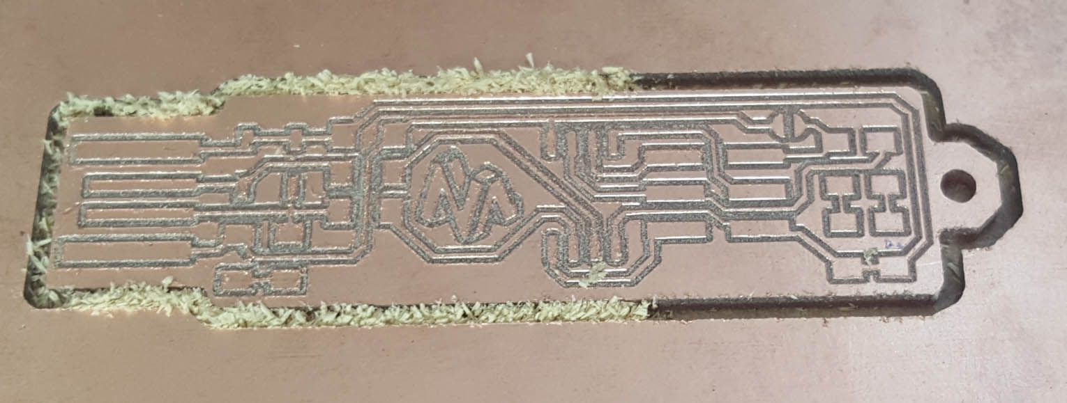
After finishing my PCB milling I decided to adjust the design by adding my logo and a key hole .
For that I adjusted the initial BRIAN design on Photoshop by doing the following:
- Change the 2 images mode from Bitmap to Grayscale to be able to modify them.
- Put them together in a single PSD file with 2 separate layers in order to see the modification simultaneously and have the same image size at the end.
- Modify the circuit board routing (by painting in black the old unwanted links between the components and drawing white lines for the new routing) in order to add a place for my logo in the middle.
- Insert the logo I made on my third week assignment and adjusting the external cutout to include a key hole
- Resave the internal traces layer(image 1) and the cutout layer(image 2) on separate files then change the image mode back to bitmap and save.
Now I will recalculate the G-code for my new PCB board in the same way I did before.
The final result.
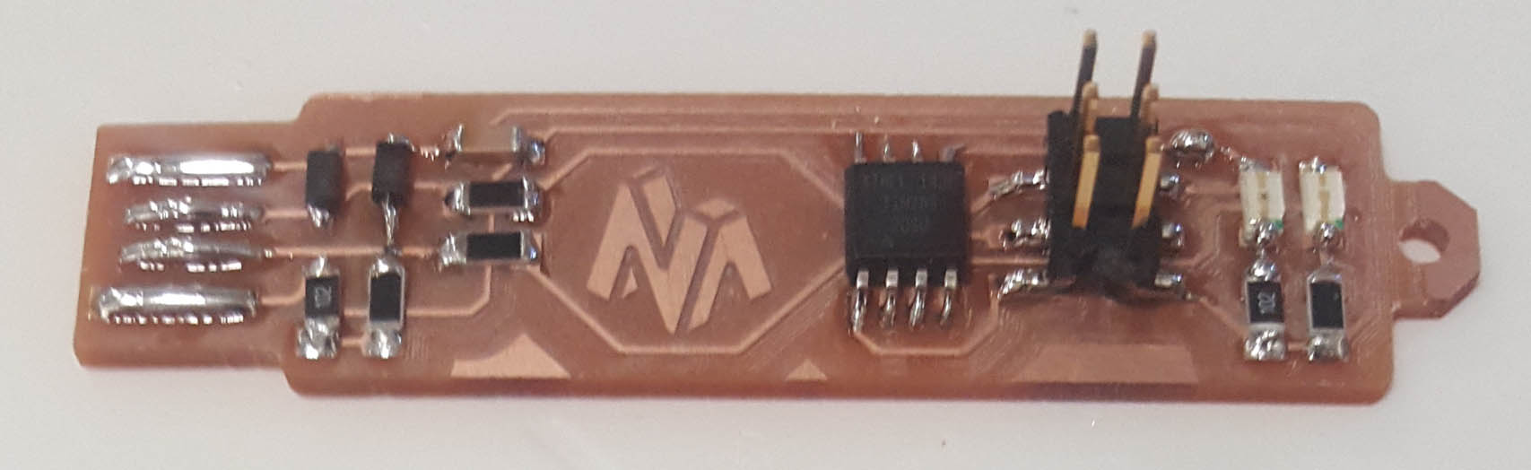
5-Soldering the Components
Obtain the components:
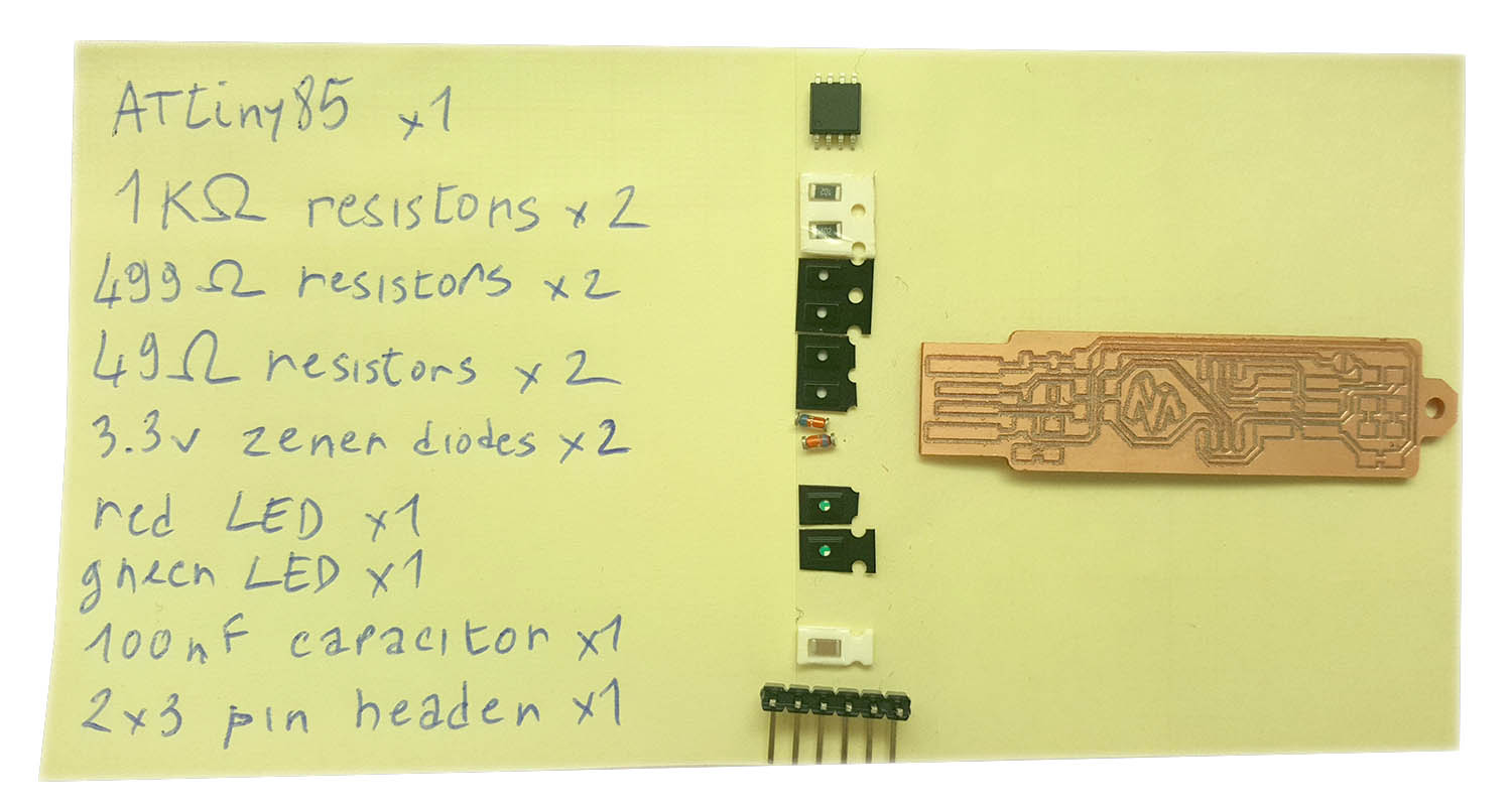
- 1x ATtiny45 or ATtiny85
- 2x 1kΩ resistors
- 2x 499Ω resistors
- 2x 49Ω resistors
- 2x 3.3v zener diodes
- 1x red LED
- 1x green LED
- 1x 100nF capacitor
- 1x 2x3 pin header
- The zener diodes are marked with a line on the cathode side.
- The LED cathodes on the PCB drawing are marked with dots and thicker lines. There is usually a green or black line visible on the cathode side.
- The ATtiny85 marks pin 1 with a dot laser-etched into the corner of the package. Pin 1 is marked in the drawing with a dot as well.
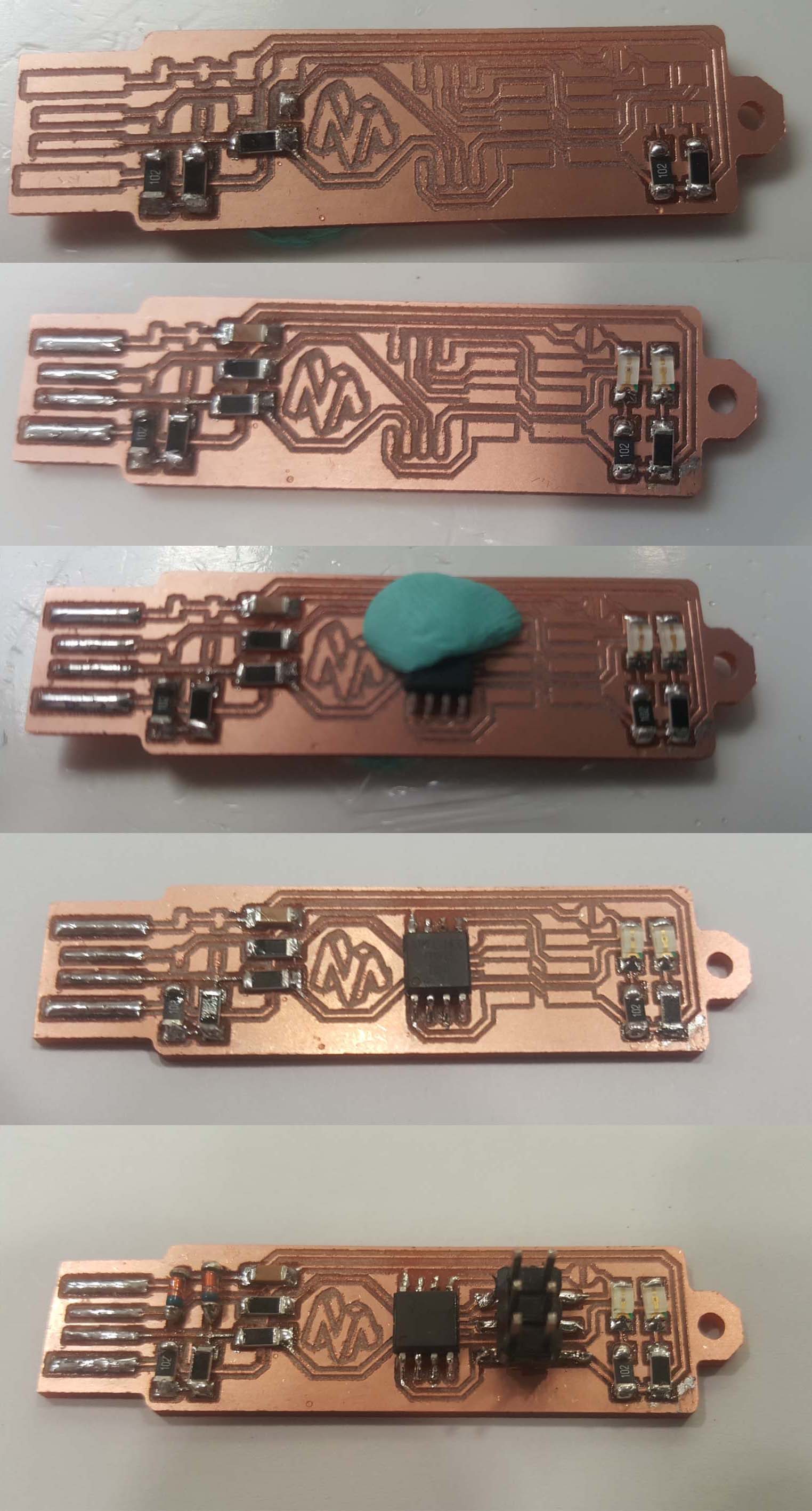
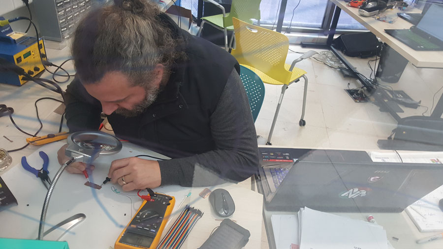
And at each step I test the board with the multimeter to check if there is any welding touching two different circuit and creating shortcut.
After finishing my second ISP. I discovered that after Programming it, the ISP wasn't recognizable as a Usbtiny so I decided to do another one.
I think that the problem was in the quality of the milling and the spacing between the wires was too thin which could lead to some short specially that it is my first experience with soldering.
So this time I will use another bit diameter 0.4 mmm instead of the 0.15mm and make 12 passes instead of 4(to make more clearance between the wires) and finally take more care of the soldering.
The new g-code.
The new milling.
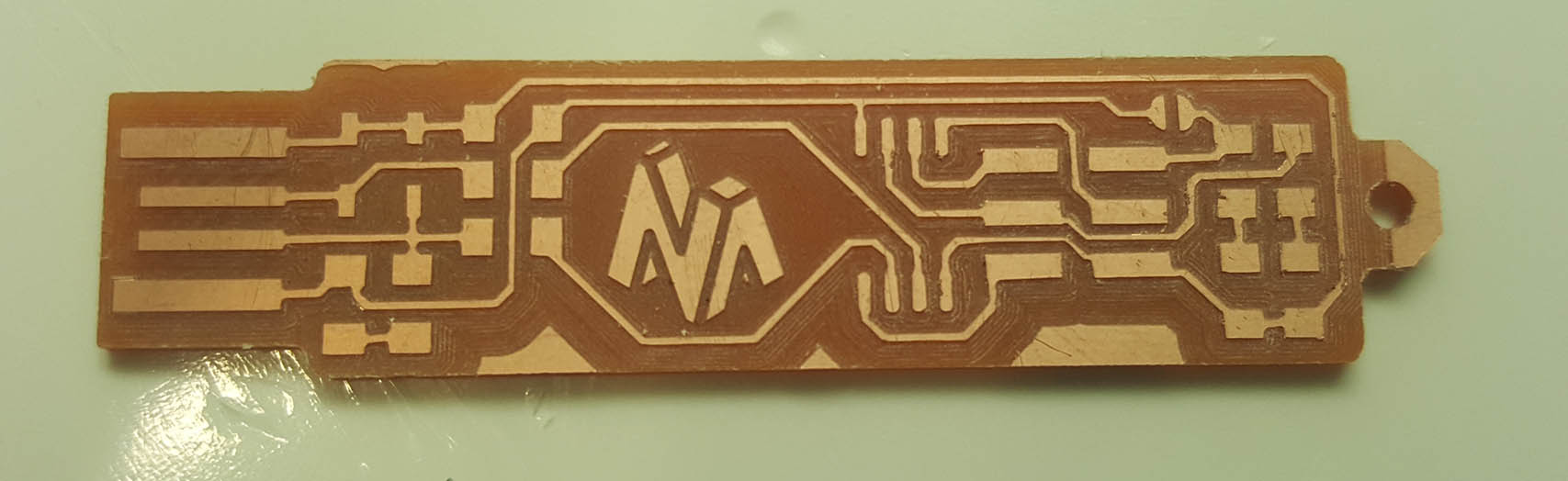
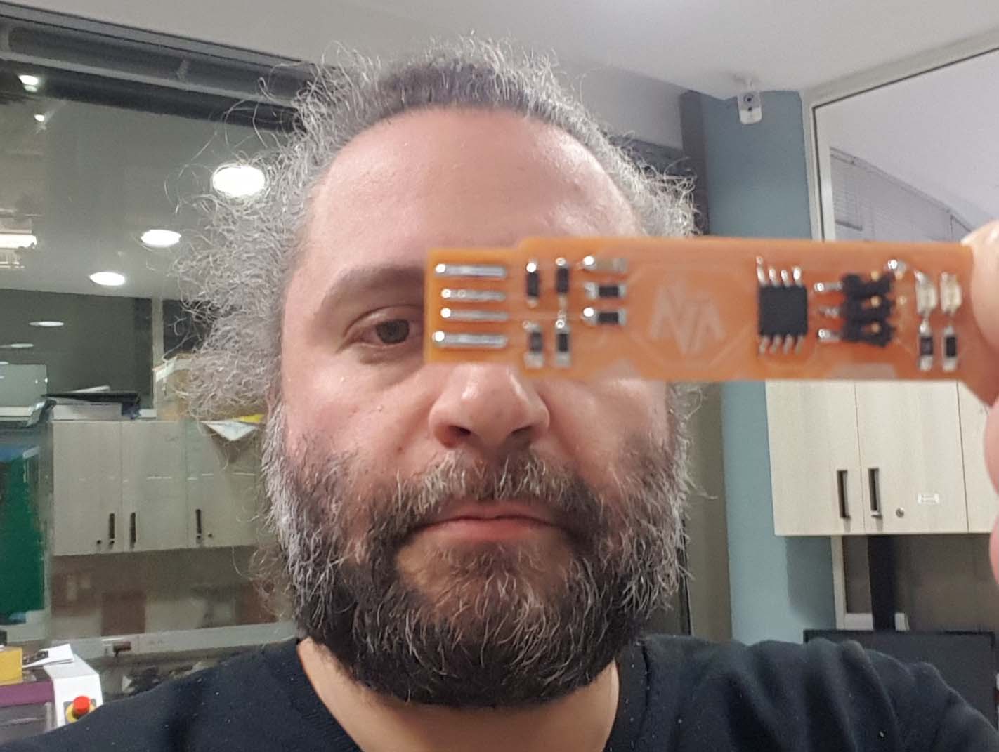
The new final one.
6-Programming the Microcontroller
After finalizing all the required hardware components needed to build the PCB, the next step is to download the Software on the ISP.For that we do the following:
- Download and open Arduino IDE software.
- In TOOLS, select the port and the Arduino model (Ardiuno UNO).
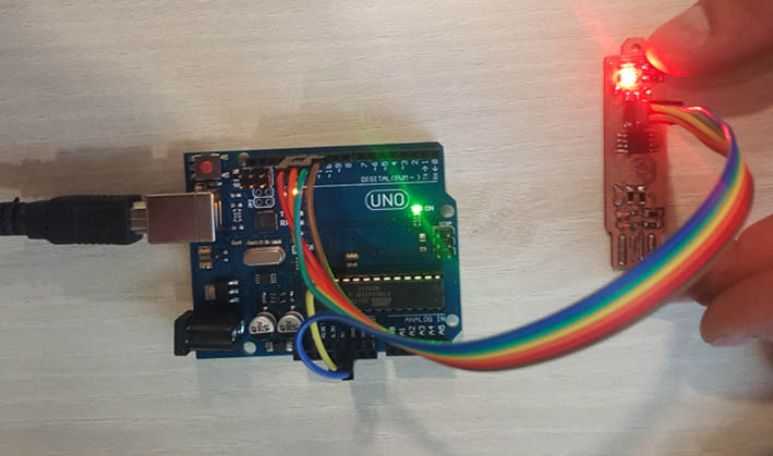
- Connect the Arduino programmer to the PC.
- In FILE>EXAMPLES open ArduinoISP and upload it.
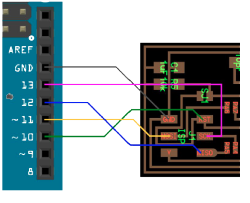
- Connect the Arduino to the ISP as shown below:
- Download the provided firmware and extract the zip file.
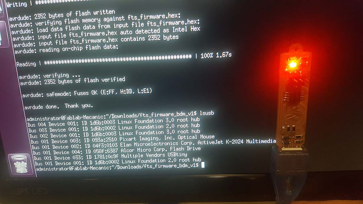
- Open the command prompt in Linux and go to the code directory.
- Enter the commands to generate a make file:
- make clean
- make
- Replace the make file with a new make file (modified makefile).
- Open the Make file with Brackets and replace MDU=attiny45 by MDU=attiny85 and save the file.
- Then Enter the following commands to load the programme on the ISP:
- make fuses
- make flash
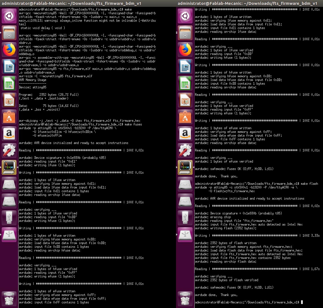
- Now, disconnect your ISP from the Arduino and plug it into the PC.
- To test the ISP type 'lsusb' in the linux command propmpt and you should see in the list Multiple Vendors USBtiny
- After verifying that my ISP is recognized I need to reconnect it to Linux and run the command "rstdisbl" ; This does the same thing as the make fuses command, but this time it's going to include the reset disable bit as well
- Finally I remove the bridge on the solder jumper and I can use it as programmer