Four Birds, One Stone
For Week7: Embedded Programming I decided to work with the super cheap PSoC 4 CY8CKIT-049 4200 prototyping kit.

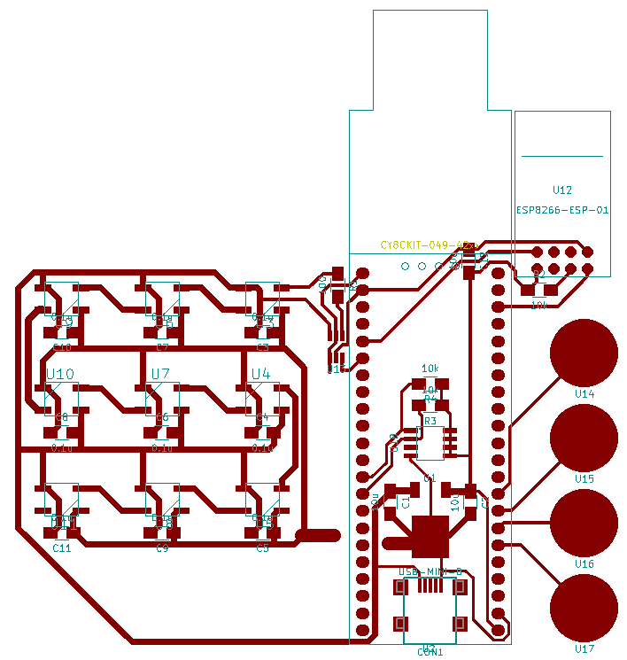
The kit itself is pretty sparse (it basically has an LED and a button), so I designed a breakout board/shield with some more interesting bits and bobs on it to play with.
Thinking ahead to upcoming assignments, I figured I could make a breakout board that should have me covered for a number of weeks. The features I wanted were:
-
WS2812 LEDs: You can read more about these nifty little RGB LEDs in last weeks post. In particular I wanted to try driving them using the UDBs of the PSoC 4, and they should cover me for "outputs" week.
-
ESP8266: The ESP8266 is a relatively new device that got makers all hot and bothered when it showed up some time last year. It's basically a super cheap chip/microcontroller for adding WiFi to projects. I picked up a few of the ESP-01 modules from AliExpress for less than £2 each. I plan on using a few of them as part of "networking" week.
-
Temperature Sensing: I had a few TMP275 chips from TI lying about. It's a temperature sensor that works over I2C and has an accuracy of 0.5°C. It should cover me for "inputs" week, and I plan on using one in the Word Clock to keep a track on the heat dissipation of the LEDs.
-
Capacitive Touch Buttons: Again, these should cover me for "inputs" week, and I plan on adding some to the clock/table too.
So that's Embedded Programming, Inputs, Outputs and Networking all (hopefully) covered using one board.
Picking A Power Supply
Because most of the devices I planned on adding only worked up to 3.6V, I decided to just run everything at 3.3V (except the LEDs). That meant adding a beefy 3.3V regulator. The ESP8266 can draw a few hundred milliamps so I went with an LP38691 from TI that I had on hand (3.3V, 500mA, easy capacitor requirements). Power is supplied from a standard USB-mini header (and directly sent as 5V to the LEDs).
The Schematic
Here's the schematic:

With the LEDs running at 5V, a 3.3V signal is slightly too low to be reliable as a logic high (5 * 0.7 = 3.5V minimum, based on the datasheet). Although I have used a 3.3V data input in the past, I've seen reports of it causing the occasional error in the LED data stream. There are a number of ways to step up the voltage, but many of them seem to be incapable of handling the data rate. Jez on happyinmotion.com has a fantastic article comparing different level shifters with WS2812 LEDs. I didn't have any of the mentioned chips on hand, but I did have a couple of SN74LVC1T45 chips. If you ask TI nicely, they'll send you some free samples. I'm yet to check the signal quality on a scope but the LEDs seem to work fine with it (which is not surprising, seeing at it's rated at 410Mbps and the LEDs work at two orders of magnitude less than that!).
Board Layout
Schematic complete, I moved onto the board layout.
Capacitor C12 (10μF) and resistor R2 (10kΩ) can probably be omitted. The capacitor is just to help with the bursty power draw of the WiFi module. The resistor is just a pull-up for the CH_PD pin (chip power-down). 10kΩ is probably a little excessive for a 3.3V pull up but it's an easy value that's in the inventory. I've seen mixed comments online about whether it's really needed or not too. Better to have a place for it and not need it, than need it and not have a place for it.
Also, note that I didn't quite manage to get a completely single layer layout. A jumper wire is needed to connect the LED ground to the USB ground. It might have been possible to use the multiple ground pins of the dev kit as a sneaky way of accessing ground elsewhere (like I did with the ground of the WiFi module) but I was reluctant to route the possibly high(ish) currents of the LEDs through the dev kit. A jumper wire from the small landing strip at the bottom right of the LEDs to the tab of the regulator was the quickest and simplest solution.
A Slight Hiccup
Our PCB engraver was out of commission for a few days so as a temporary measure I set up an equivalent circuit on a breadboard.

Neil might hate breadboards and think that they're useless but in my opinion they're just another tool. Yes, they can become a mess of wires. Yes, the capacitance between tracks is pretty massive. But, for quick prototyping with low-frequency signals (by that I mean analogue signals < 1MHz and digital < 8MHz-ish), they can be a really useful tool. The breadboard worked perfectly and meant I could work on the software while waiting for the PCB engraver to get fixed.
Back On Track - Cutting The PCB
I'm currently in the process of writing a full tutorial on using the Denford. It will probably only be useful to people in our lab, but I'll link to it here when it's ready.
Our lab technician Lindsey lay her healing hand on the Denford PCB Engraver and everything was fixed. Now I could ditch the breadboard and get a PCB cut.
I opened the Denford PCB Engrave software and imported the gerber for the board. Even though the board passed a design rule check with a clearance of 0.4mm (the diameter of the bit I was using), the Denford software warned of a possible isolation problem.

Frustratingly, the software doesn't say where the isolation problem might be. I added those nice red circles myself, after scrolling around all the tool paths to see where the isolation issues were. The problem area was around the SOT23-6 package for the SN74LVC1T45 level shifter. Even though the cutter wouldn't pass through the gap, I figured that the diameter of the tool was enough that the copper would still get cut. Thankfully, this turned out to be the case.
Once again, I had to modify the KiCad drill file to be compatible with the Denford software. The resulting preview shows that the drill hits are all the in the right place.

Some milling and drilling later, I had a pretty nice looking PCB. The image below was taken before I even de-burred or washed the board. With the PCB cut, it was time to stuff and solder.

Experimenting With A Kapton Solder Paste Mask
I took the opportunity to try a new method of applying solder paste: laser cutting a stencil out of Kapton. I taped a sheet of Kapton to some sacrificial plywood I had kicking about (although in hindsight, acrylic might have caused less burning around the edges). After playing around with the laser settings (I found that 70/17/5000 worked well for our 40W Epilog) I exported the solder mask from KiCad as an SVG and imported it into CorelDRAW. A grand total of 32 seconds on the laser later, I had a solder mask.

It took a while to remove all the tiny cut-outs, but even the really close cuts like on the pins of the USB connector held their shape really well. The next step was to secure the stencil over the PCB. I just used some masking tape.

I used an old card as a spreader, and tried to keep the paste as even as possible. I think I could have got a better result by securing the stencil on the same "level" as the PCB. By that I mean use some spare copper clad around the edges of the PCB and stick the masking tape to that, instead of straight to the table. If you look closely in the picture, you can see that the edges of the PCB caused the stencil to bulge slightly in the middle. This resulted in the paste in those areas not having quite as consistent a height or defined outline as the pads near the edges of the board.
Once the paste was as even as I could get it, I carefully removed the stencil.

The result was a LOT better than when I tried to apply the paste by hand. The definition around the USB connections wasn't great, but I figured I could clean any bridges up later with a soldering iron.
Very carefully, I added all the components to the board. The paste is slightly tacky, so it helped to hold the components in place.

I double (and triple) checked that I had all of the components orientated the right way and then gently moved the board to the reflow oven. Because I had had some issues the previous week with not all of the paste reflowing, I used a reflow profile with a slightly higher maximum temperature.

Seven minutes later, I had an (almost) perfect board.

If you look closely, you can see that the pins of the LEDs and capacitors nearest to the bottom edge still didn't quite reflow properly (the joints are dull, not shiny). I think this was due to the placement of the PCB in relation to the bulbs of the reflow oven. In the future, I'll probably tweak the reflow profile again to try and get a more consistent reflow. As I suspected, the USB connector pins had also bridged. I used the soldering iron to reflow the paste that hadn't quite made it, and then used some solder wick to un-bridge the USB pins. I soldered on the header sockets for the dev kit and ESP-01 by hand too.
Overall, I think the process went quite well. I probably wouldn't bother doing it for a board with any fewer components on it than this one did though.
Programming The Board
You can read about how I programmed the board to control the LEDs in the following post:
I'll add links to posts about the temperature sensor, capacitive touch buttons and the ESP-01 as I write them.
Get The Files
WARNING! Because the breakout board is designed to work at 3.3V, you CANNOT USE THE CY8CKIT-049 4200 DEVELOPMENT KIT WITHOUT MODIFICATION. Unmodified, the dev kit is powered directly from the 5V VUSB on the USB-UART. There are a few options:
-
Unsolder the resettable fuse from the USB-UART (the fat resistor-looking chip between VUSB and R7). This will power everything from the 3.3V regulator. I also used the control panel in the Cypress USB-SDK to tell the USB-UART that it had a 3.3V VUSB, so it could disable it's internal regulator (see all the settings I used below). This is the option I went with. Note that this option only works for a 3.3V supply.

-
Snap the USB-UART board from the main dev kit board. When you want to program the dev kit, remove it from the breakout board, connect it to the USB-UART, program it, disconnect the kit from the USB-UART and then plug the dev kit back into the breakout board. I avoided this route as it would have been a massive waste of time.
-
Break the VDD connection between the boards (either by snapping the USB-UART off and not adding a connection pin for it, or by removing the 0Ω resistor on the dev kit) and then add voltage level translation between the USB-UART and the PSoC 4 RX. The other direction (PSoC 4 TX) doesn't need shifted, as the chip on the USB-UART board can be programmed to accept down to 2V as a logic high when powered at 3.3V.
-
Cut a trace on the under side of the USB-UART, after the VUSB pin of the chip is supplied but before and other power pins are supplied. I think the best place to cut would be on the bottom side of the board, immediately after the via that brings VUSB power to the under side of the board. This would allow the chip to have it's VDD connected to the target device's power so that no voltage translation would be necessary, making it incredibly flexible as a generic USB to UART/I2C/SPI/CapSense/GPIO. I never tried this as I only had one dev kit on hand and if it was a bit too...permanent a test considering I wasn't sure it would definitely work or not!
-
Program the board using the SWI interface and ignore the bootloader entirely. I'm probably going to end up going this route using the PSoC 4 BLE kit I have as the programmer. Partly because it will be useful to have a debugger, but honestly just so that I don't have to bloody power cycle the dev kit while holding the user button in every damn time I want to re-program the board. If you don't have one if the Pioneer kits, you could try using one CY8CKIT-049 to program another PSoC4.
Now that you've been warned:
- Here are the KiCad files for the breakout board.
- The board has been verified to work with the LEDs. The temperature sensor, ESP8266 and CapSense features should be considered experimental until I've verified them.
As usual, the files given here might be out of date. The latest-and-greatest can be found on my GitHub.
Comments
comments powered by Disqus