4. ELECTRONICS PRODUCTION
This week assignment is to learn about PCB (printed circuit board) fabrication .Creating the board with a precise milling machine and soldering the tiny SMD [surface mount] components on it. This week task was really overwhelming and tiring. I had an idea about commercial electronics but this includes more in depth knowledge about electronics. Milling PCB and soldering such tiny components were also completely new for me.
Tasks for this week :
Group assignment: Characterize the design rules for your PCB production process
Individual assignment: Make an in-circuit programmer by milling and stuffing the PCB, test it, then optionally try other PCB processes
Fab ISP
Fab ISP is an in-system programmer for AVR microcontroller which is designed for production within a fab lab. It allows to program the microcontrollers on other boards.
For this purpose, ATTiny microchip is used as the chip for programming and it is the brain of the fab ISP board.
The microchip used for this exercise is ATTiny 45.
PCB making steps
A] Milling the board
PCB milling is also known as isolation milling, which refers to the process of removing areas of copper from a sheet of PCB material to recreate the signal traces, pads, as well as structures based on patterns from a digital circuit board plan called a file of PCB layout. PCB milling process is subtractive process.
I selected the Brian’s version of Fab ISP called FabTinyISP for this week. It was much easier to understand tis version than other fab ISP versions.
STEP 1:
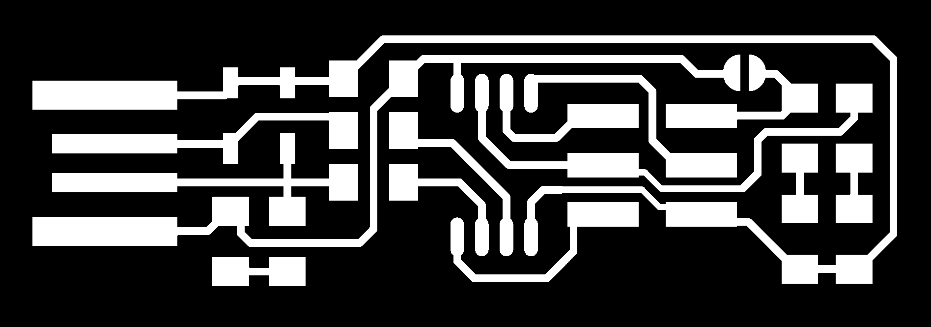
Download the PNG image of the traces and board outline from Brian’s documentation

STEP 2:
Preparing the file for milling
a] Preparing DXF file in corel draw
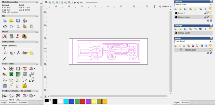
The PNG image of traces and outline is combined and converted to vector outline in corel draw.
PCB file preparation in corel draw
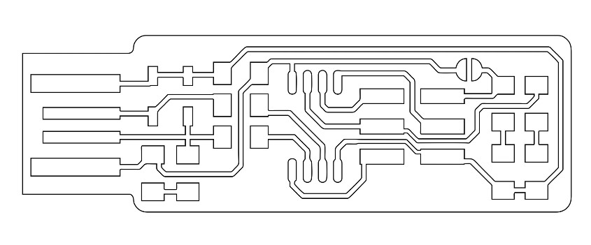
PCB file preparation in corel draw
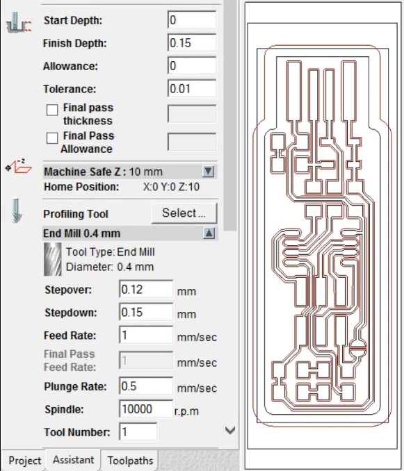
b] Setting the CAM settings in artcam
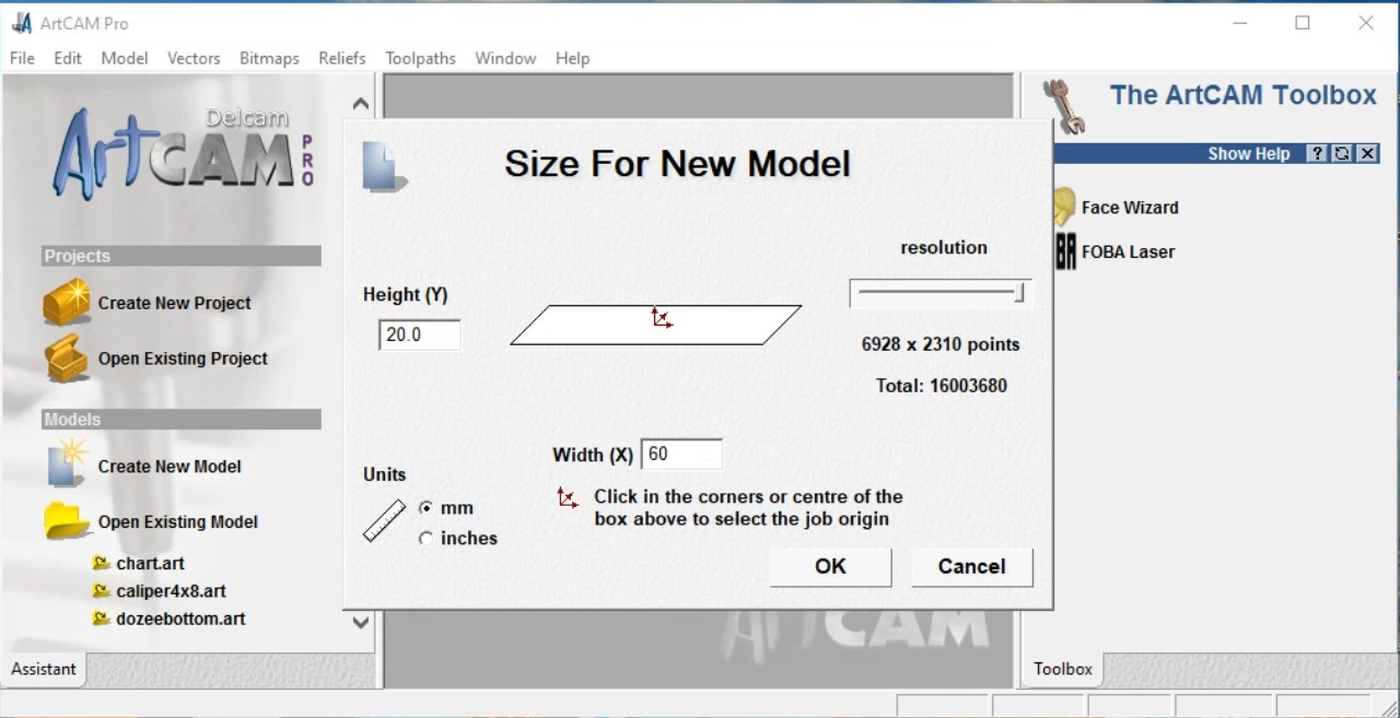
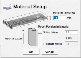
1] Setting up the approximate size of the model so that the model fits in the page when imported.The centre of the page should be selected as the job origin.
2]Importing the DXF file into artcam [go to vector > import]

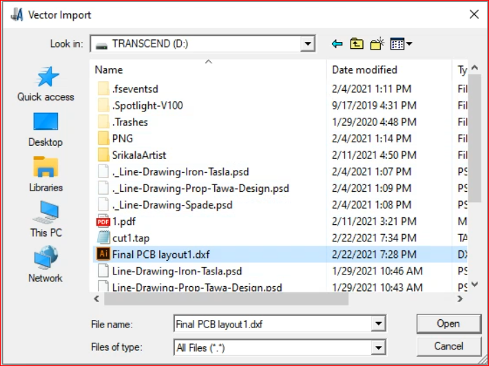
3] After clicking open, the following window will open specifying the file units and other parameters. After checking everything,click OK.
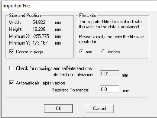
4] Imported file
After importing , multiple lines should be checked before proceeding just to make sure everything is correct.
5] Creating 2D area clearance
The icon highlighted with green circle should be selected for area clearance. [Go to ‘Toolpath’ in the right bottom > area clearance icon]
![]()

6] Outside cut
The icon highlighted with blue tick should be selected for profiling. While , specifying the parameters for outside cut the outline should be selected.
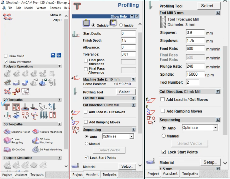
Correction: In the above image , spindle speed is 8000r.p.m. Rest of the parameters are same.

7] Final outcome [Area clearance + Outline cut]
![]()
8] Saving .tap file
To save the .tap file [Go to Toolpath on the top menu > Save tool path as]
.tap files convert the instructions to G and M codes that is understandable by the machine.
Two ‘.tap files’ should be saved for the traces and the outline cutout in a convenient location because our CNC machine doesn’t have automatic tool changing option.
STEP 3:
Milling the PCB
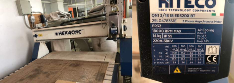
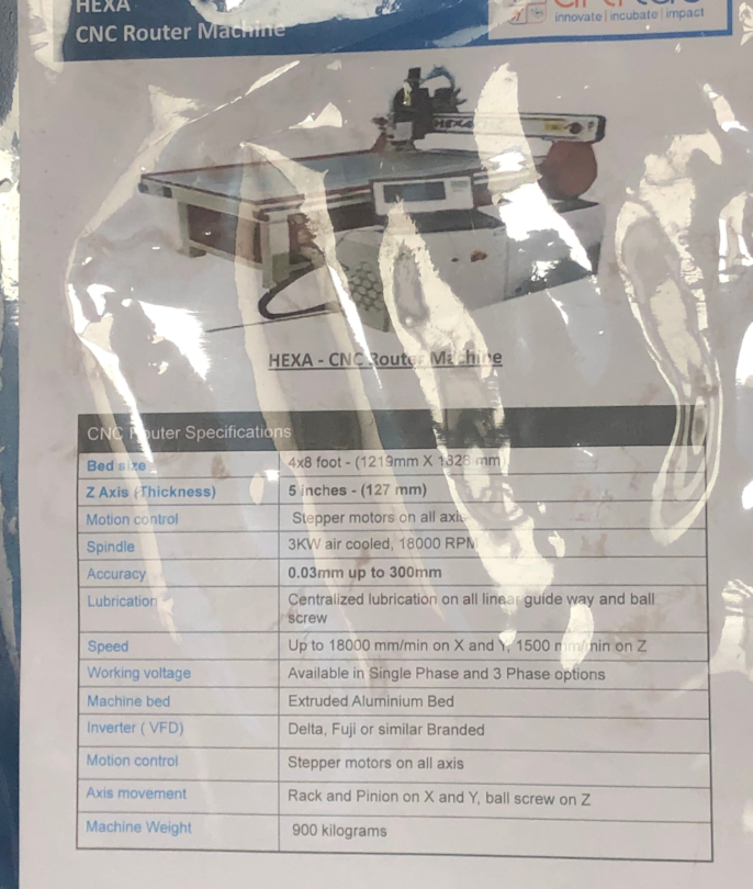
This is the machine I used for milling my PCB. Roland would have been easier but that machine was under service so we used this for milling the PCB. Collet size of the machine is ER32.
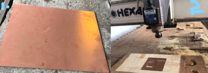
Picture 1. The material used for milling PCB is single layer copper clad. I’m making a surface mount device so used a single layer copper clad [ Thickness : 1.5mm ,thickness of copper layer on top: 0.15mm]
Picture2: Levelling the machine is very important while milling.
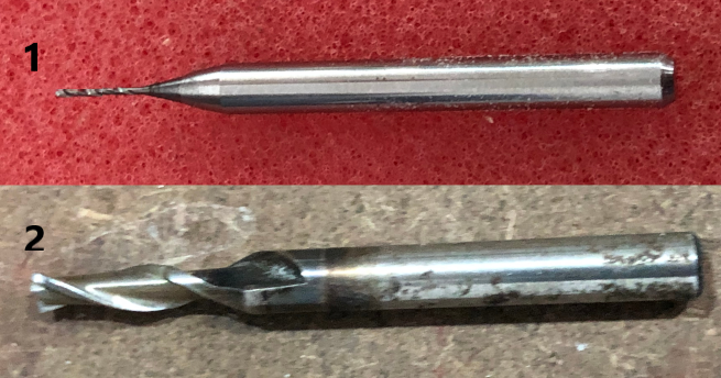
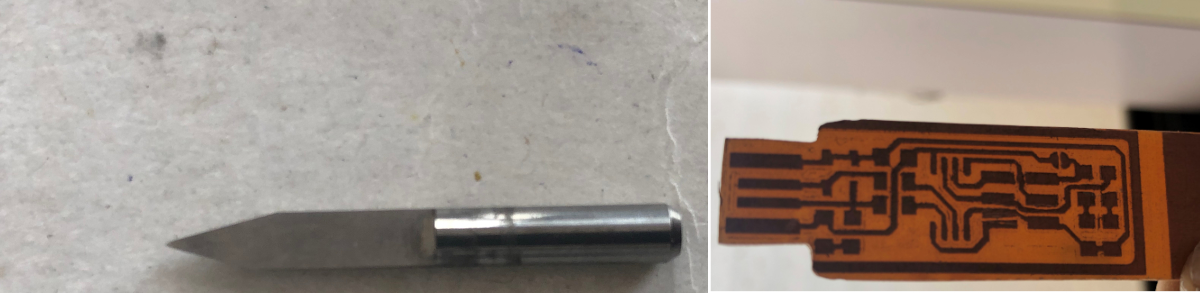
These are the bits used for milling my PCB.
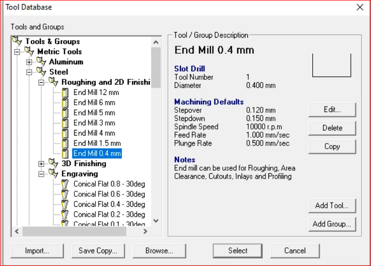
Picture1: 0.4mm end milling . Used for making the inner traces.
Picture2: 3mm end mill. Used for making the outside cut of the PCB.
The tool has to be fixed with a spanner. The collets also should be cleaned with grease for smooth functioning. The tool should be placed inside the collet such that it is least prone to breakage. The tool should be carefully removed. One has to keep their hand or some soft material like sponge so that the tool won’t break.
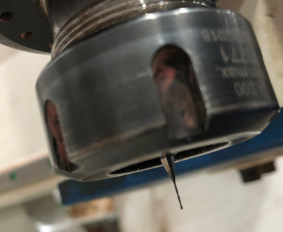
After the tool is placed, the machine should be brought to the work axis. The .tap should be loaded in the hexa CNC software. Then after starting the milling, the feedrate should be increased slowly to 100% . The feedrate depends on the work that is being done.
The below picture shows the simulation of the inside traces and the outside cut.

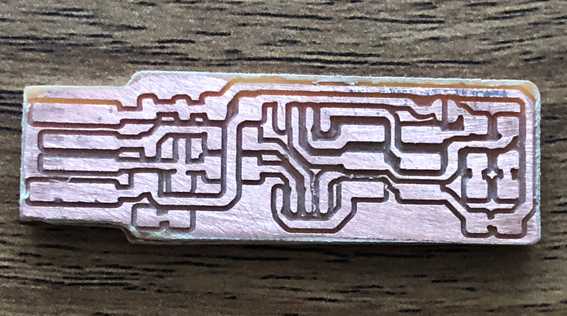
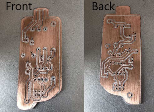
FINAL PCB
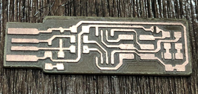
The PCB, USB is thin and won’t fit into the computer port. A small piece of extra material should be glued at the back just to give it some extra thickness.
Characterization of the design rules for PCB production process
BOARD 2

Difference between area clearance and profiling
The area clearance of toolpath is used to clear an area of material based on the boundary of a selection of vector artwork. This toolpath is ideal for clearing unwanted areas from a block of material. For ex: Here, the copper area is cleared. Only the copper traces are left. This makes it easier for soldering.
The profile toolpath is used to machine inside, outside, or along the boundary of selected vector artwork. This toolpath is ideal for cutting out letters and shapes from a material block. For ex: Here ,the traces are made by cutting through the copper clad material.
Art cam parameters explanation
BOARD 3
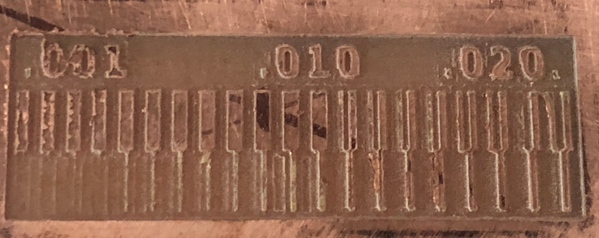
I milled another board with a 0.2 mm 20 deg conical engraving bit.
The right side image shows the finl board.
BOARD 4
Double layer Through hole PCB.
There were few problems while milling this PCB . We had through hole components. Milled a through hole board in a double copper clad material. I personally prefer SMD board but this one was a good learning experience.
BOARD 5
Chemical Etching method
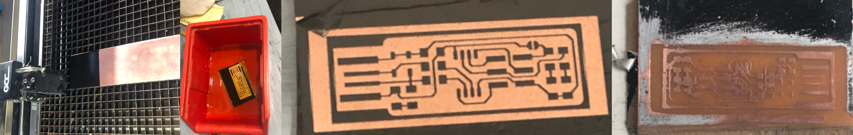
The PCB is kept in ferric chloride + H20 [1:1 ratio]. However , the PCB didn’t come out well because the ferric chloride concentration was not sufficient.
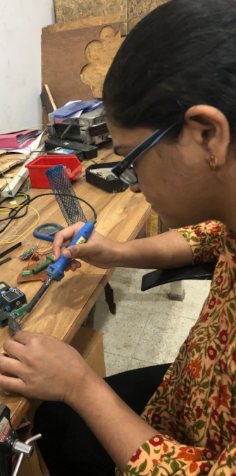
Soldering and stuffing
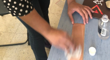
After , milling the board has to be sanded slightly and should be cleaned neatly with isopropyl alcohol with a clean cloth.
Isopropyl alcohol is the best compound to use on water-sensitive devices like computers, laptops or any other electronic devices because it evaporates and dries almost instantly.

Component List :
1x ATtiny45 or ATtiny85
2x 1kΩ resistors
2x 499Ω resistors
2x 49Ω resistors
2x 3.3v Zener diodes
1x red LED
1x green LED
1x 100nF capacitor
1x 2x3 pin header
The SMD package used is 1206. This indicates the size of the SMD package. It is 12 mills by 6 mills.[0.012*0.006 inches]
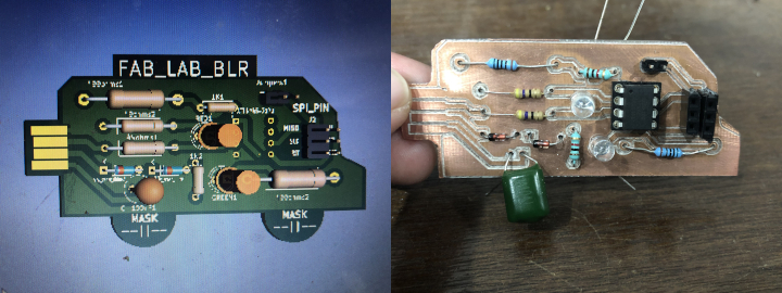
Schematic of FAB ISP
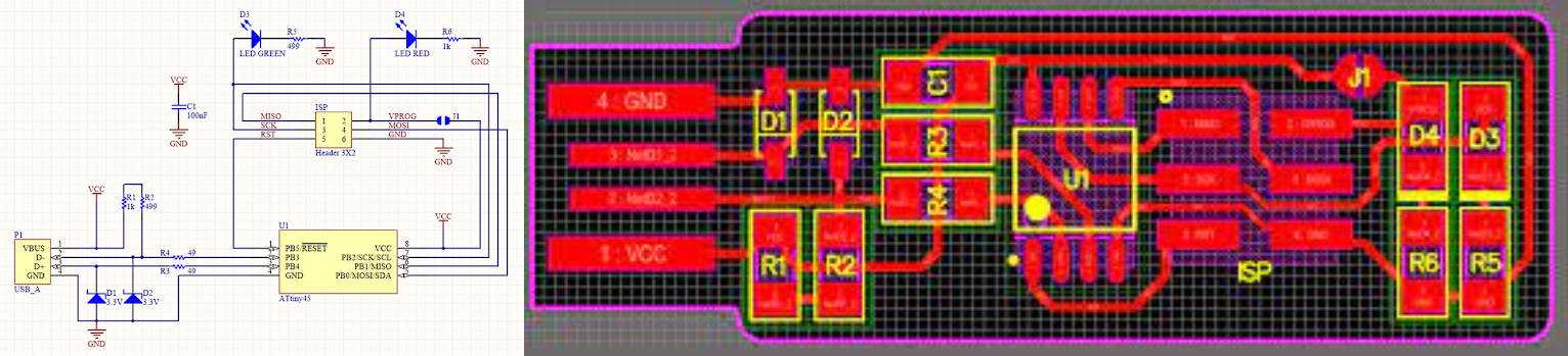
The schematic helps in knowing the placement of components. Especially , for diodes like LED the placement should be according to the polarity [ anode and cathode].
Soldering station and solder materials
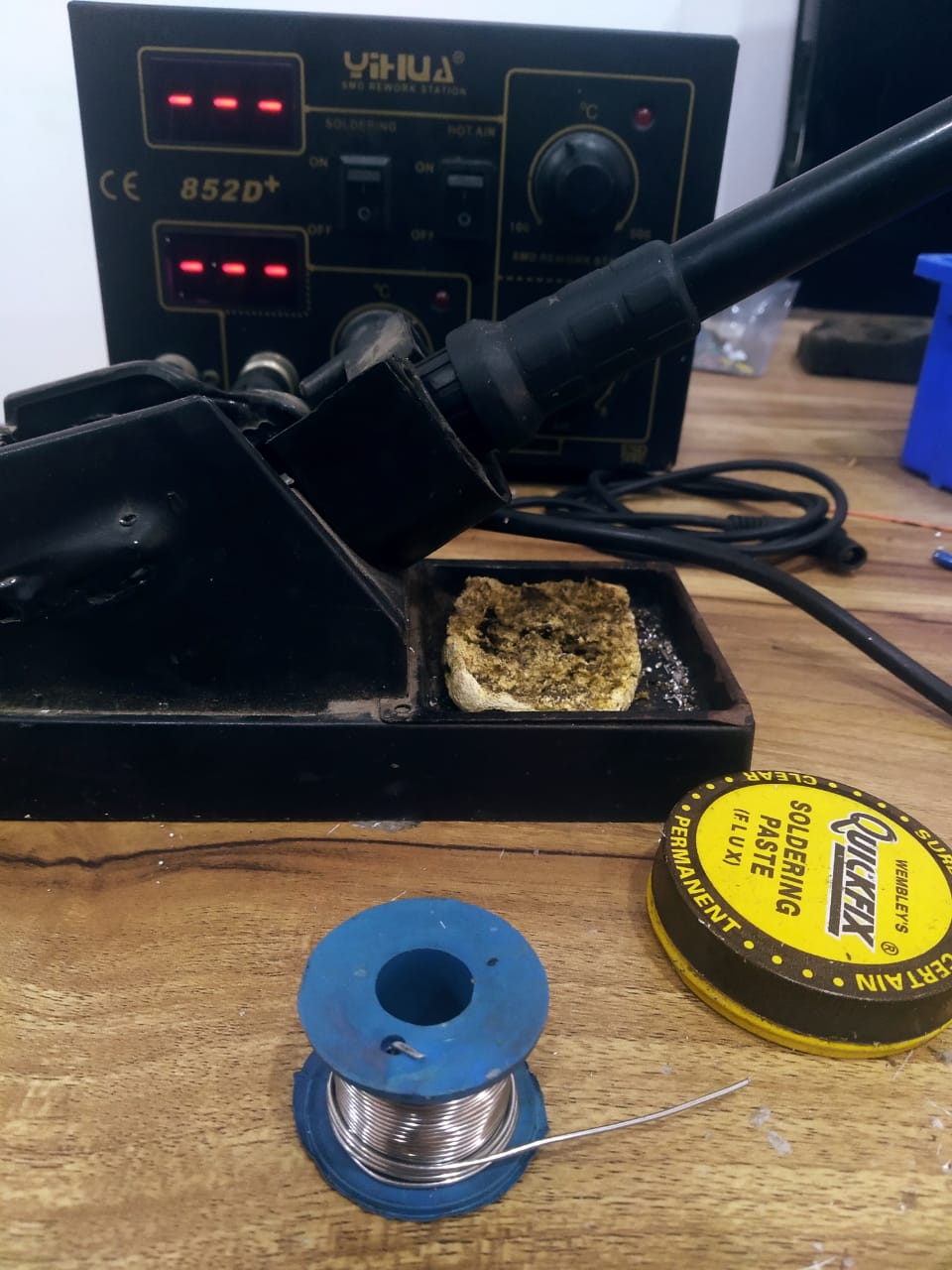
Method 1: To solder SMD , I took very little amount of solder lead, put it on the pads on the PCB. Then using a tweezer, I placed a the component and used the hot air gun for reflow.
soldering SMD with hot air tips
Method 2: Put little amount of lead on the pad. Place the component in the position using tweezers and place the solder on the pad such that the solder lead melts [ this is called solder reflow] and the component stays in it’s place. Once the component is fixed on one side, the other side can be soldered in the same way.
The soldering should be smooth and correct consistency.
Method 2 is much more effective for beginners because hot air needs the correct temperature and techniques.
Solder iron cleaning tips
The solder temperature should be around 342 to 350 degree celsius. Hot air temperature should be around 250 to 300 degree celsius. The Solder tip should be regularly cleaned with a wet sponge or a steel wire. This will help in removing unwanted dust and dirt from the solder tip. Even flux can be used to clean the solder tip. Flux is a chemical cleaning agent used before and during the soldering process of electronic components onto circuit boards. Flux is used in both manual hand soldering as well as the different automated processes used by PCB contract manufacturers. The main purpose of the flux is to prepare the metal surfaces for soldering by cleaning and removing any oxides and impurities. Oxides are formed when metal is exposed to air and may prevent the formation of good solder joints. The flux also protects the metal surfaces from re-oxidation during soldering and helps the soldering process by altering the surface tension of the molten solder.
Desoldering
Desoldering helps in removing excess solder.Desoldering pump is really useful for desoldering. Desoldering with desolder pump
Checking the connectivity of the PCB
A continuity test tells us whether two things are electrically connected: if something is continuous, an electric current can flow freely from one end to the other.
If there’s no continuity, it means there is a break somewhere in the circuit. Continuity is one of the most useful tests for electronics repair.
This page explains clear instructions to perform connectivity test
Soldered board
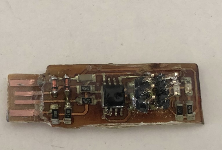
The board got slightly messed up after applying araldite. I thought it would protect the copper from oxidation but the result didn’t turn out that well.
Process of flashing program to programmer
I have used ‘arduino uno’ as my programmer to program my fab ISP.
Things to be done when setting up arduino as a programmer :
1] Open arduino IDE.
2] Click files > examples > Arduino ISP . Open this code and upload to your arduino before running flash.
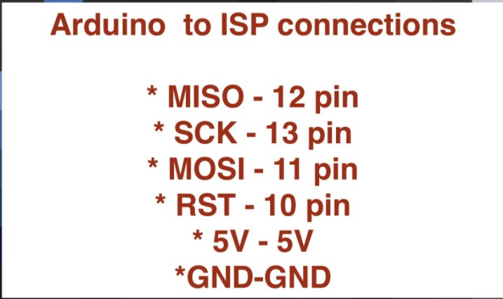
After uploading, connect ISP pins of arduino to ISP pins of ISP Programmer
ISP : Arduino
SCK : pin 13
MISO : pin 12
MOSI : pin 11
RST : pin 10
5V : 5V
GND : GND
Note
1] Before running “flash”, make sure you edit the makefile with corresponding programmer.
2] Before running “flash”, connect a 10uf eletrolytic capacitor between “Reset and GND” of arduino board.
For example: If you are using, arduino as a programmer, you need to set the programmer in the Makefile to arduino
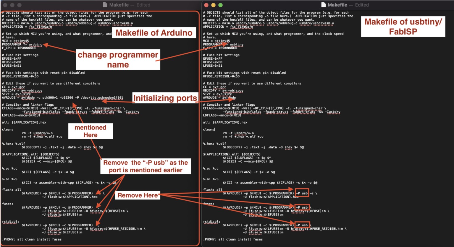
After setting the makefile it is time to run “make flash”, “make fuses”, “make rstdisbl”
Here is the video of execution of “make flash”, “make fuses”, “make rstdisbl”…
Note
Before executing these commands , a solder bridge should be made in the “solder-jumpers”
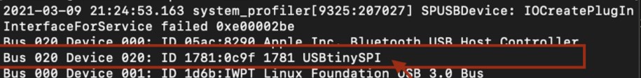
After executing you have to remove the solder brigde… Like this …
After removing the solder bridge, if you want to see detection of ISP-Programmer.. Just type
“lsusb”
If you get some error after running “lsusb”, just type this command.
brew install lsusb
This will install the “lsusb package” and after this, you will be able detect your ISP-programmer… like this..
Now MASK-ISP is ready to program any microcontroller.