6 - Electronics Design
This week is about designing a PCB board with a micro-controller and understand it by displaying the in and output. First find out how our lab equipment works. Than individually redesign a ‘Hello World’ board, Mill it, Solder it and program it. We will use A LED an LDR and button as input and output.
extra credit: simulate its operation
How can I use this in my final project?
- I need to know how logic works
- I need a PCB for WiFi (ESP)
- I need a PCB to heat the wires (30 mosfets)
- I need to use serial communication to drive these mosfets with one dataline
- I need
The steps for this assignment
- 1. Group: use the test equipment in your lab
- 2. Draw the schematics to redesign the ‘Hello World board’
- 3. Design the PCB
- 4. Mill the board
- 5. Program the board
- Files
- Final conclusion for this week
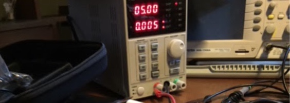
1. Group: use the test equipment in your lab
Use the test equipment in our lab to observe the operation of a microcontroller circuit board read all about this group assignment
2. Draw the schematics to redesign the ‘Hello World board’
We had instruction using KiCad, but since I didn’t like the UI so mutch I tried Fusion Eagle. To get started is really hard, just like Fusion 360. I watched this video to get the basics.
Steps
| 0 | Ad the fab Library to eagle | I downloaded the Fab library and followed this nice manual ‘how to install an Library (including footprints) in Eagle’ |
| 1 | Here are the components | 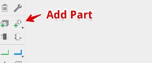 |
| 2 | When ready with placement press escape | 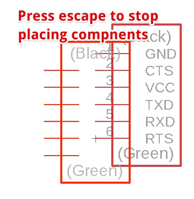 |
| 3 | Drawing wires works simular | 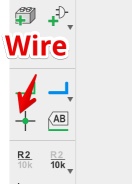 |
| 4 | While drawing, rightclick is rotate. Escape= end of wire | 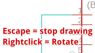 |
| 5 | To connect wires you use Labels | 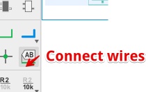 |
| 6 | You Add the labels to the wires, not the components | 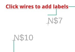 |
| 7 | First select the name change | 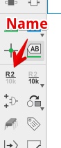 |
| 8 | Then click the wire to rename the wire | 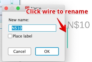 |
| 9 | 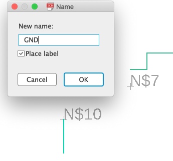 | |
| 10 | If the name you enter is similar to a name on one of the other wires. The wires will be ‘connected’ | 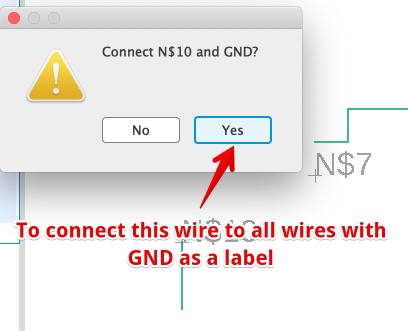 |
| 11 | First select a component, than in the information panel, enter the value | 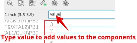 |
| 12 | Final check of the scemetitics. Printed | 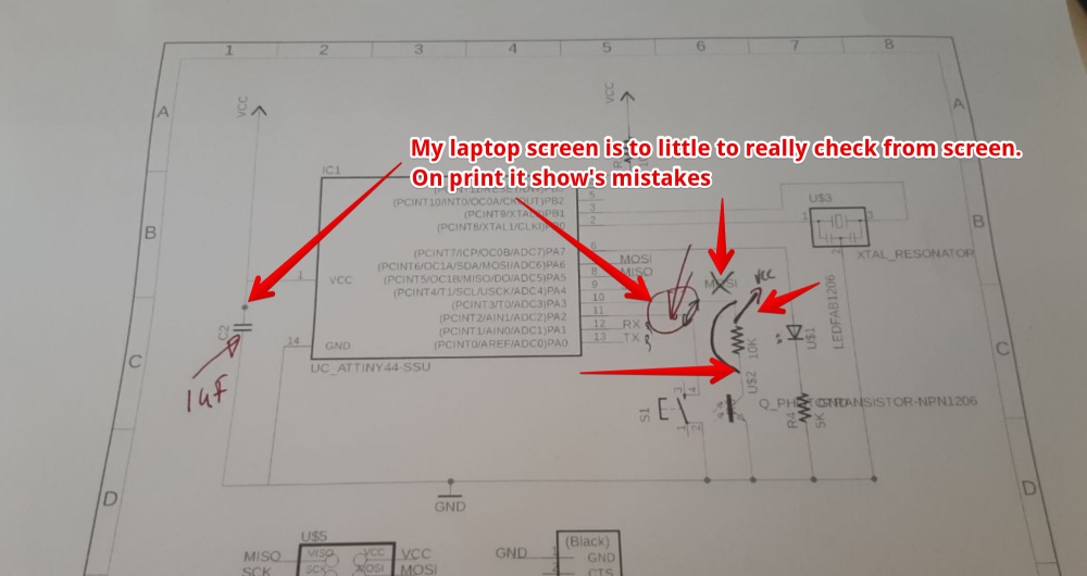 |
Mistakes/mental notes
- It took me a few hours to find out eagle was not working with shortcuts. You first activate the command line mode (use CMD-L). Then type the command. Most used commands are
- Net: for a wire
- Label: label wires to ‘connect invisible
- Move: move a part or wire
- I didn’t understand the connection between a label and a name… So I first added labels and than changed the names in the labels. To find out a ‘name’ is the text in a ‘label’…
- The workflow for Eagle is: select a action, then apply this action to all components/wires. The steps I took are more from the mental model of the object. Next time I will first put ALL down > name/value ALL > wire ALL > move ALL etc.
The result 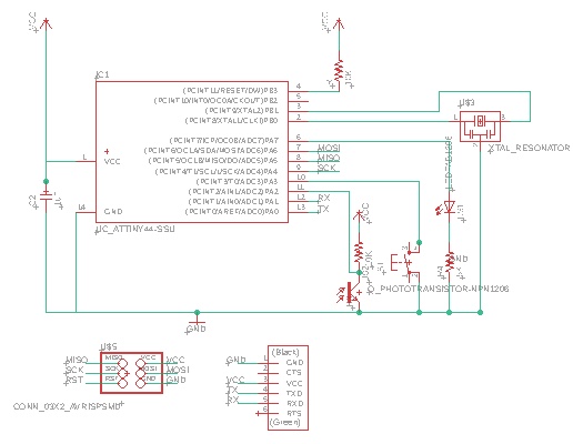
3. Design the PCB
| 1 | First try placing the components. I started with the component with the most legs, placed it in the center | 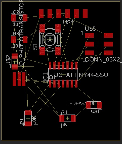 |
| 2 | The name labels are really disturbing, so I wanted to remove them | 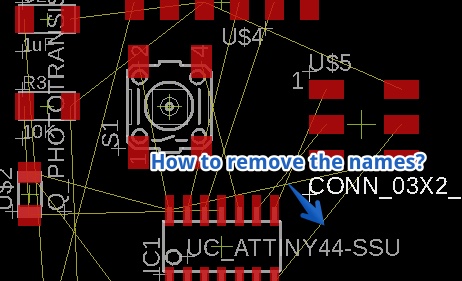 |
| 3 | You can alter the view settings by First selecting the component with Group and disable the Value or name | 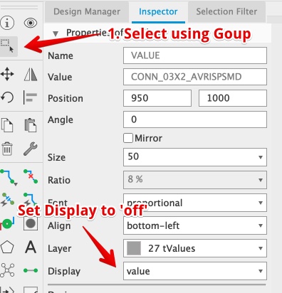 |
| 4 | It took me some time to find out why I was so frustrated selecting components (with the Group tool). You have to Click the Cross to select a component | 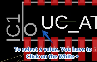 |
| 5 | My fist atempt of many, just ONE Airwire to go | 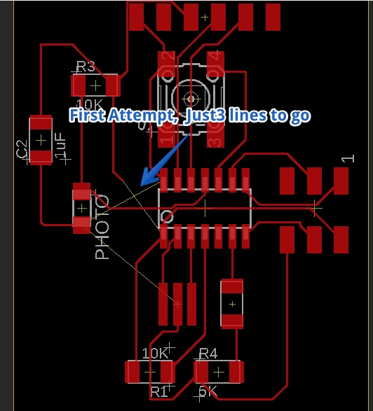 |
| 6 | I found out switching off the labels (name and or value is a lot better in the layers) | 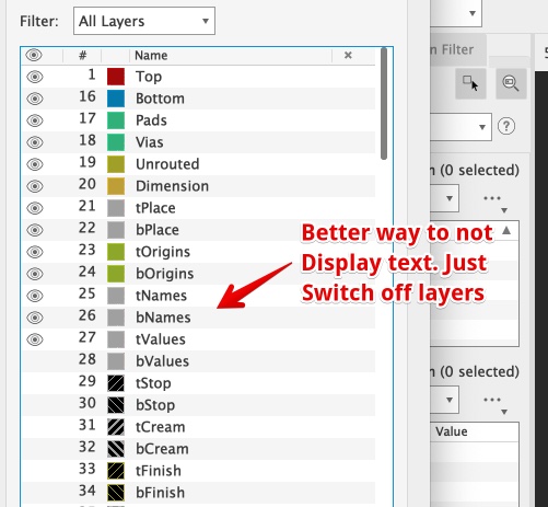 |
| 7 | I got rid of the labels, but still no luck in generating a PCB | 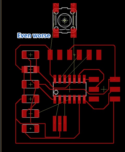 |
| 8 | Looked for strategies to place components. But besides first placing the components with most connections and than starting to draw VCC and GND, I found not Much | Autodesk PCB placement tips for beginners |
Problem - traces too narrow
I managed to create a board. But the traces are too narrow 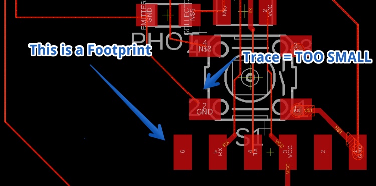
So I had to remove all the wires and I desided to set the Design rules for the board (Henk explained this for Kicad but not for Eagle).
3.1 Set the Design Rules for the board
| 1 | Tools > DRC | 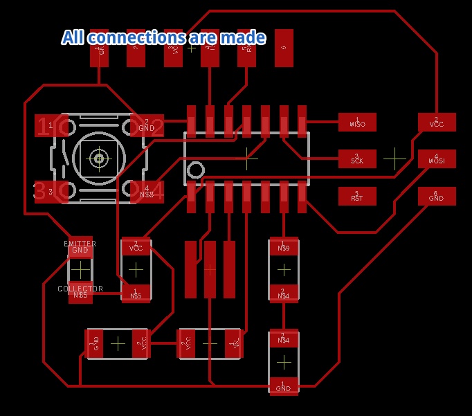 |
| 2 | Feedback error: One ‘Airwire’ | 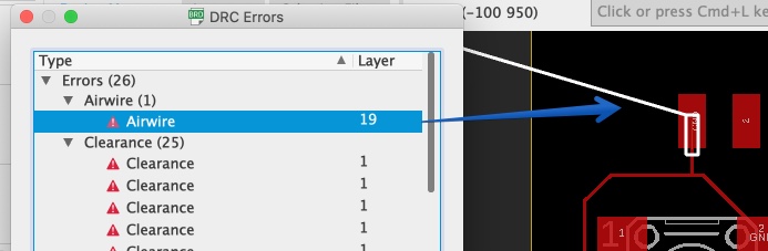 |
| 3 | The GND wire was not connected |  |
| 4 | I re-draw the wire with ‘Redraw Airwire’ and this error was solved. Then only 25 Errors remained… | 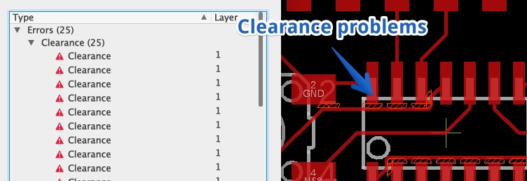 |
| 5 | I used the page of Catherine Blanchard |  |
| 6 | After redrawing I went to Tools > DRC… > Check. A new error appeared. A small piece of copper was behind the VCC. I removed it. | 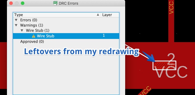 |
| 7 | Again did the DRC check. No more Errors. But this is very subtle in the UI. |  |
| 8 | Before export as PNG, make the label visible you would like to export | 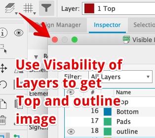 |
| 9 | Match the resolution of the exported image to the resolution of the milling machine | 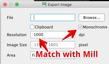 |
I used these settings for DRC 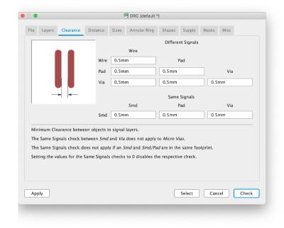
Lessons learned
- When not setting the design rules, wiretraces and distance between traces will not work for our specific milling machine. First set the Design rules, than draw the board!
mental note
- In eagle use the command line (most used move, name, value, trace, delete, ripup DRC)
The result 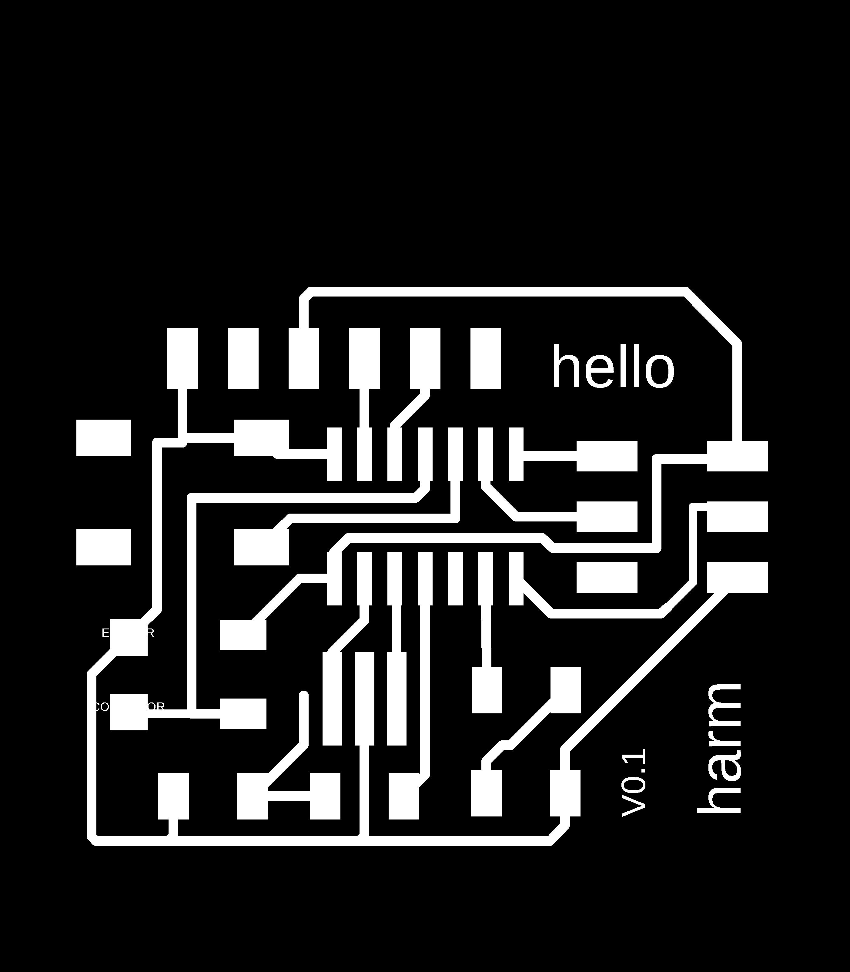
4. Mill the board
For the milling of the boards I used the steps of week 4
| 1 | While milling the mill went to the outside of the board. It turned out the board was to big. | 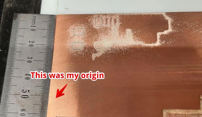 |
| 2 | Measuring the board in Eagle and in real life it turned out my board was twice the size | 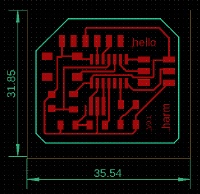 |
| 3 | The Same image in Eagle 35,6 x 45.21 mm and in Mods 71.20 x 81,43 mm!!! So exactly twice the size. Both settings are 1000 dpi | 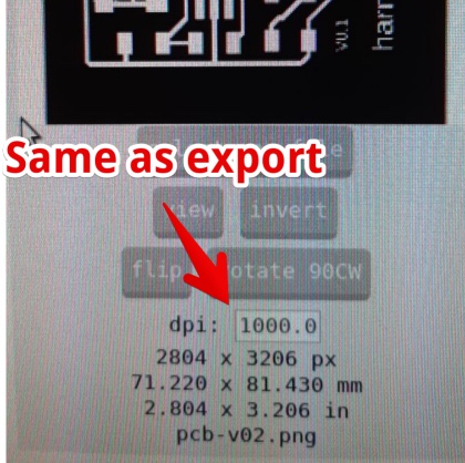 |
| 4 | This post in autodesk mentions the same problem | |
| 5 | I changed the setting in the Image MOD to 2000 DPI. Now the dimensions are right. | 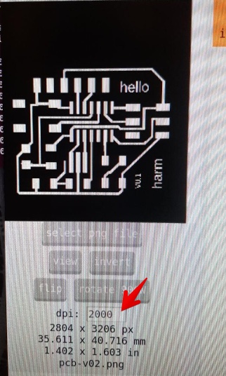 |
| 6 | milling the traces went well, But milling the outline didn’t work well. I forgot to lower mill enough. The head was in its lowest position. So I put the Mill down and started the outline again. | 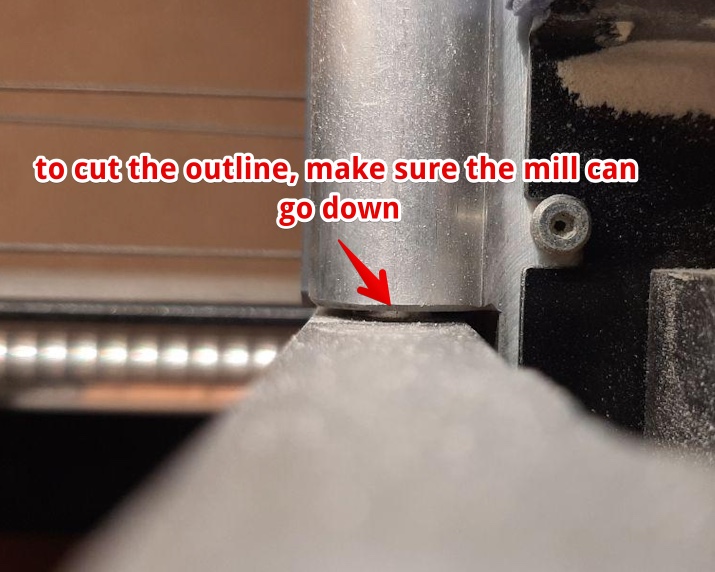 |
| 7 | The outcome was disappointing Two pads where connected. | 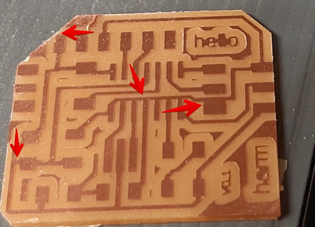 |
| 8 | I should have been looking in the MODS: VIEW. Before milling | 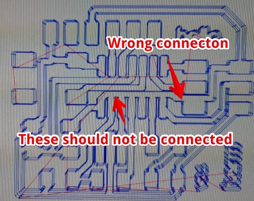 |
| 9 | I moved the traces a bit and now the mill will divide the copper. | 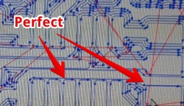 |
| 10 | But I had a board and not so much time… So for the first version I Used a knife to cut away the false copper I used the Multimeter to make sure I succeeded to insulate the traces. | 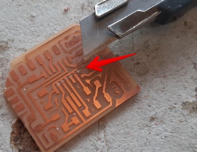 |
Thanks to my global evaluator I found out one of the connections I had to cut was coused by text over the pad. Next time I will use these settings to make names and values smaller: 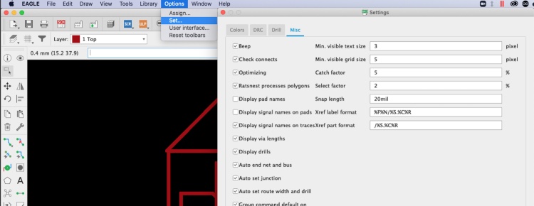 Thank you Yuichitamiya!
5. Program the board
| 1 | I looked at the scematics of my AttinyISP and the Hello44Harmboard to see how I should connect these board via a Flatcable. | 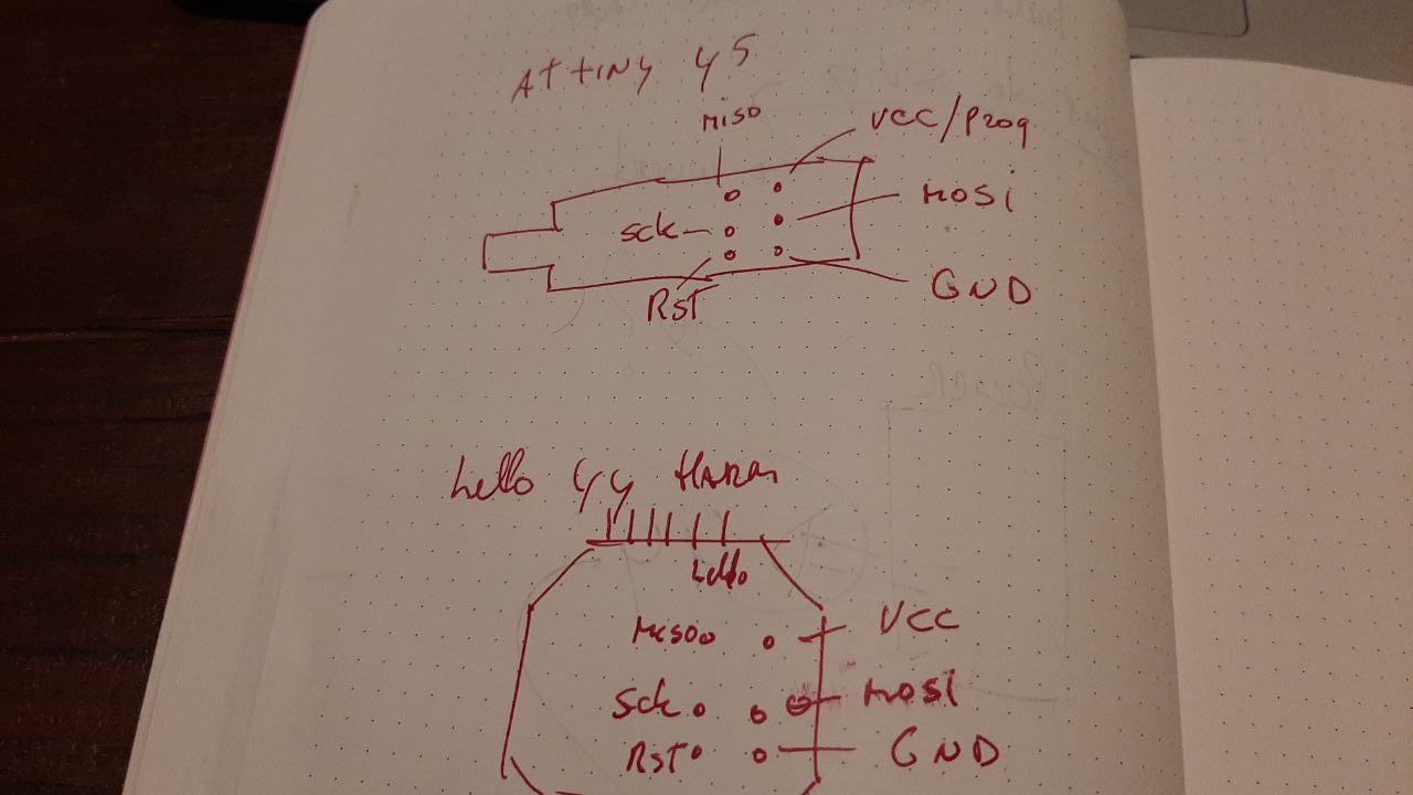 |
| 2 | This should be the way to connect both boards | 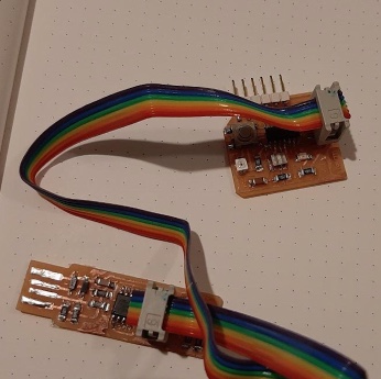 |
| 3 | [I looked at the steps Joey van der Bie took last year | 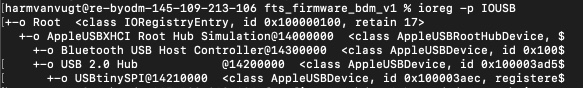 |
| 4 | Connected the board to my USB 2.0 hub and tested. But It could Not talk to the ATTiny44 Hello board ;-( | 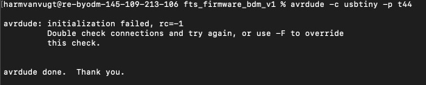 |
| 5 | I looked up how the MiSo Mosi etc pins of the 44 should be connected in the 44 Datasheet | 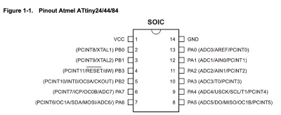 |
| 7 | And put the pin number next to the PSI header. I used the continuity setting on the multimeter to see if the pins on the PSI header on the SPI where connected to the ATtiny44 chip | 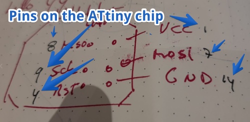 |
| 7 | I looked for the connections, But the RST was not connected to the board. | 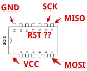 |
| 8 | IN the schemetics the Reset was simply not available | 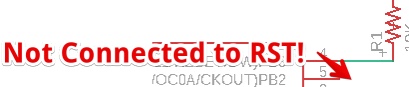 |
| 9 | I Added the label for the next version of the board | 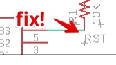 |
| 10 | But first tried if I could fix the board with a Wire | 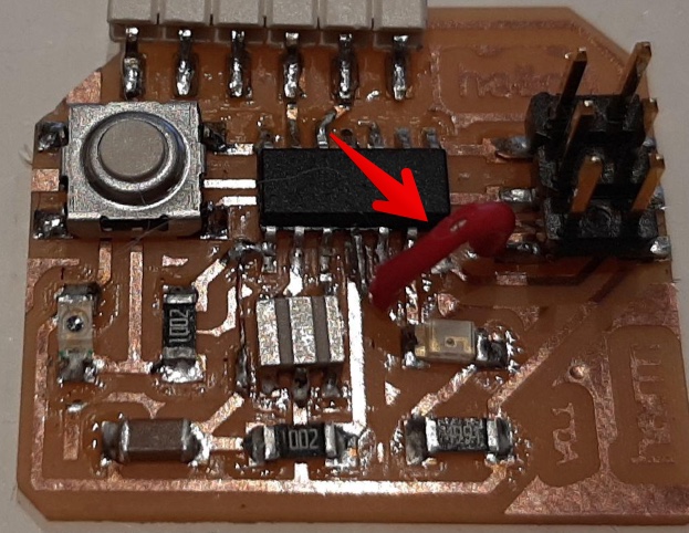 |
| 11 | Tried again “avrdude: Error: Could not find USBtiny device (0x1781/0xc9f) “ | 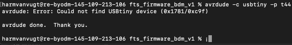 |
| 12 | I tried ioreg -p IOUSB to see if my laptop could ‘see’ the TinyISP. Even this didn’t work anymore | |
| 11 | DON’T connect without the USB2. 0 adaptor!! | 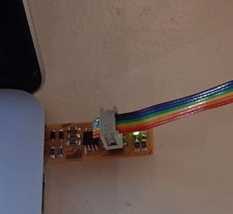 |
| 12 | This is the right way | 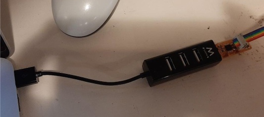 |
| 11 | Now it works! | 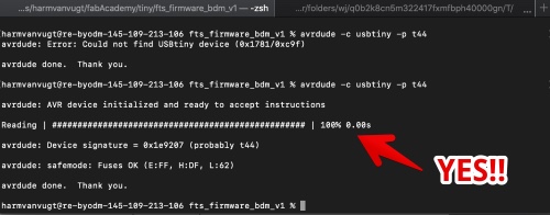 |
5.1 Test the board (Using Arduino)
I wanted to test the board and the sensors and actuators. So I tried to program the board with Arduino IDE. But Didn’t know how to address the LED, Button. Thanks to Hyjin’s page I managed to find the library where the setting are. But only for the 84. With some help from Henk we found the 84 is a bit better. More memory etc. But pin-outs are the same on the WIKI page of the ATtiny
In the header file ‘pins.h’ file in /Users/harmvanvugt/Library/Arduino15/packages/attiny/hardware/avr/1.0.2/variants/tiny14 I found:
// ATMEL ATTINY84 / ARDUINO
//
//                           +-\/-+
//                     VCC  1|    |14  GND
//             (D 10)  PB0  2|    |13  AREF (D  0)
//             (D  9)  PB1  3|    |12  PA1  (D  1)
//                     PB3  4|    |11  PA2  (D  2)
//  PWM  INT0  (D  8)  PB2  5|    |10  PA3  (D  3)
//  PWM        (D  7)  PA7  6|    |9   PA4  (D  4)
//  PWM        (D  6)  PA6  7|    |8   PA5  (D  5)        PWM
//                           +----+
I looked in my schematics of the board and this should be the way to address the components:
| Component | connection on chip | Code (pin) |
|---|---|---|
| LED | PA7 | 7 |
| Photo | PA2 | 2 |
| Button | PA3 | 3 |
To test the button, the LED and the Photo Transistor I made a code where:
- Default the LED is on
- But if you press the button, the led blinks. With the frequency of the light on the Photo transistor.
In code it looks like this:
int ledPin = 7;
int buttonPin = 3;
int knoppie = 0;
int sensorPin = 2;

void setup() {
  pinMode(ledPin, OUTPUT);
  pinMode(buttonPin, INPUT_PULLUP);
}

void loop() {
  knoppie = digitalRead(buttonPin);
  int sensorWaarde = analogRead (sensorPin);

  if (knoppie) {
    digitalWrite(ledPin, HIGH);
  }  else {
    digitalWrite(ledPin, HIGH);
    delay (sensorWaarde / 50); //I divided the sensor-value by 50, it was trail and error.
    digitalWrite(ledPin, LOW);
    delay (sensorWaarde / 50);
  }
}
At first this code Didn’t work. The led was simply ON. I remembered I had a lot of doubt when soldering the Photo transistor. I could choose one out of 3 and couldn’t rationale which was the correct one. With some help form Tessel she found the data-sheet and since the package should be 1206, I picked the one with 1206 package.
Hero Shots
Not working? Youtube to the rescue
Files
Final conclusion for this week
Conclusion on the process of electronics design
- Don’t rush: The process of electronics production is a slow one. Every tiny mistake will have huge consequenses at the end.
- Work in series: don’t jump from one step to the other in the process. First complete AND check the step and than continue with the next one
- For a next electronics design I have to really rethink how I set up Eagle. Now the grid and the traces do not perfectly align with the components.
- Electronics production is Hard, how can Electrics be so cheap???
Biggest Mistakes and lessons this week Other from the ons described in all the steps in this page ;-)
- In Eagle: Set the Design rules before designing the PCB
- In the Mods for milling: Check the traces before starting the Miller
Wat went really good
- When I finally understood the idea behind Eagle is was okey to work with.
- I liked the soldering
- I liked the end result, the LED blinks depending on the quantity of light
My concerns
- If I have to produce a complex board, with Internet connection in my final project, I need mere than two weeks to complete this. So fall-back would be an ‘almost ready’ WiFi micro-controller and custom made boards for input and output…