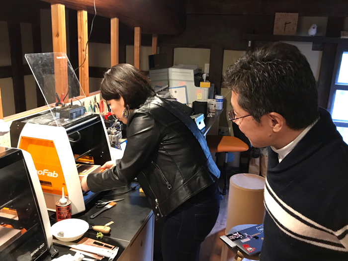
4. Electronics Production
This week I made a in-circuit programmer by milling the PCB, soldering the electrical components, and write a program for having the programmer write a program to the micro-controllers.
Assignments
group assignment:
- Characterize the design rules for your PCB production process.
individual assignment:
- Make an in-circuit programmer by milling and stuffing the PCB, test it, then optionally try other PCB processes.
X. Group Assignment
- Leveling a surface of the stage
- Create a pass (transform from .png file to .rml file)
- Decide the position
Link to group session page.
X. Individual Assignment
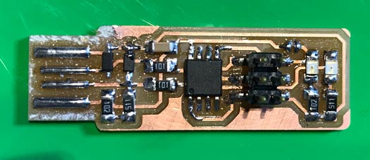
I made a Fab TinyISP (Tutorial) as the programmer.
Materials
- PCB (Printed Circuit Board)
- Electrical Components
- Solder
Tools
- Milling Machine: SRM-20 (ROLAND)
- Endmill
- Programmer
1. Milling
Working flow on milling is define the initial position of endmill (X-Y-Z position) -> create a .rml file -> Milling.
In group session, leveling the surface was already finished.
So the details of the operations of each process are written in our group assignment.
Define the initial position of endmill
Please go to our group assignment page about the detail process of setting up the initial position.
Create .rml file
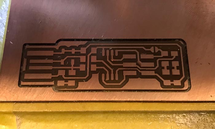
Download two .png files from tutorial/PCB Fabrication/Traces and Outline Cutout. Traces is the pattern image of the ISP, and Outline Cutout is the outline of the ISP.
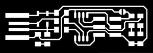

Fig. Traces (Left), Outline (Right)
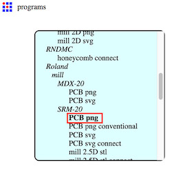
Open a mods. Please follow: right click -> click ‘programs’ -> click ‘open server program’ -> click ‘SRM-20: PCB png’.
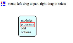
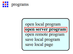
Main program of MODS opened. please follow the process in the order of the number in the picture.
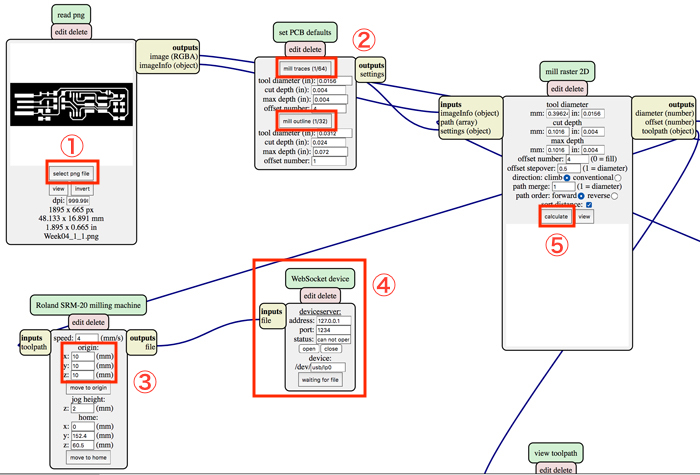
① Read Traces .png file.
Note
You need to mill the pattern first because if you mill the outline first, the PCB that cut down might move away when you mill the pattern.
② Set to 1/64.
Note
1/64 endmill was used when you mill the pattern, and 1/32 endmill was used when you mill the outline.
③ Make sure that the offset was inputted as “0”.
If the number was inputted, the milling position was offset during the milling.
④ Delete WebSocket device module and create Save file module
by right-clicking -> modules -> open server module -> file: save.
(because SRM-20 were not connected online. I needed to save .rml file to my PC and send to the PC connected to SRM-20 through USB memory.)
⑤ Push Calculate button to create a .rml file.
Note
You can check the tool pass of the mill.
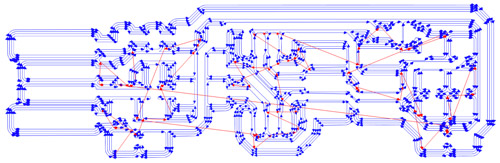
As the calculation finished, the tool pass of your PCB was opened. You can check whether one tool pass is connected with the other ones. If it is not opened automatically, you can see the same tool pass by clicking ‘view’ button next to ‘calculation’ button on MODS.
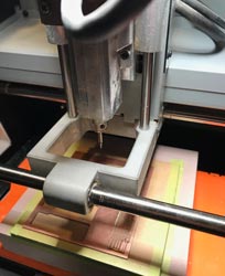
Milling
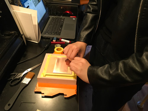
Set the PCB on the stage.
PCB were fixed on the stage by double-sided tape. Make sure that PCB is parallel to the side of the stage.
Firstly, attach the endmill 1/64 first.
Use 1/64 to cut testpattern and 1/32 to cut interior.
Don’t tighten a screw too tight because the screw was deformed and cannot be used.
And then, open VPanel for SRM-20.
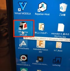
Open VPanel for SRM-20 and send .rml file through USB memory to the PC connected to SRM-20.
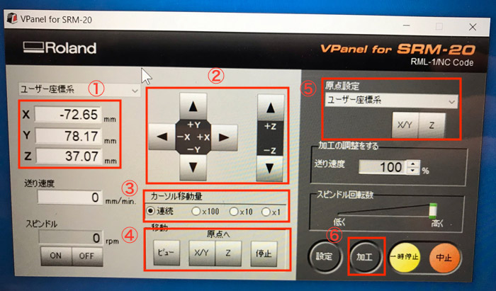
① Show the current Position of an endmill at X-Y-Z directions.
② Move an endmill position.
③ Control how much an endmill move per one click of ②.
(連続 = Continuous, x100 = 1 mm, x10 = 0.1mm, x1 = 0.01mm)
④ Move to the origin position.
⑤ Set the origin position.
⑥ Read .rml file and start milling.
Set up the origin position.
First, I set X-Y origin position.
In the image, the origin position are set at marked location. Move the mill to the appropriate position.
Click X/Y button at ⑤ to set X/Y origin, and then close a mill to the surface of PCB like a the below image.
After close a mill to the surface of PCB, loosen the screw that fixed the endmill and touched the endmill to the surface of PCB very softly but do not float the mill because when it mills, the Z-position is a little bit down.
And then, tighten a screw again.
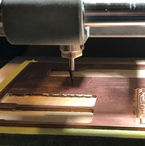
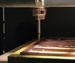
Finally, mill PCB!
You can mill also the out frame at the same way.
Finished
My thoughts
It needed only a little time to set up the milling than I expected. So easy and safe way to make PCB pattern (if you can adjust the initial z position properly. If can’t, you have to try again and again, and the endmill might be broken…)
2. Soldering
Components & Circuit Diagram
FabTinyISP
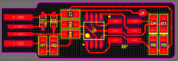
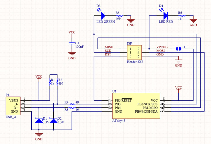
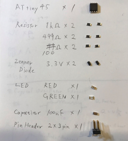
1x ATtiny45
2x 1kΩ resistors
2x 499Ω resistors
2x 100Ω resistors (Alternate to 49Ω in tutorial)
2x 3.3v zener diodes
1x red LED
1x green LED
1x 100nF capacitor
1x 2x3 pin header
Note
For diodes(LED and Zener Diodes), make sure that they are mounted at the correct polarization. Confirm their polarization with their data sheet, do not judge it in the images on the pages.
Cutting the extra copper
Cut the part of extra copper using ultra sonic cutter.
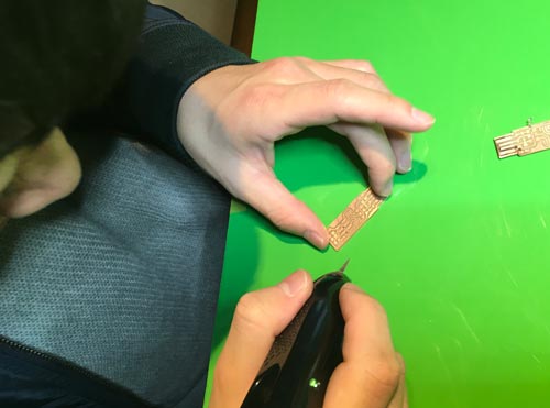
Bad sound~♪
Soldering components
There are many tips with soldering. I recommend to learn them with actual experience. Just try it!!
Make sure to bridge J1 part by soldering to program using a programmer.
Tip
Neil told us Solder the components with small height. And for my experience, I feel it’s easy to solder them from center to surroundings.
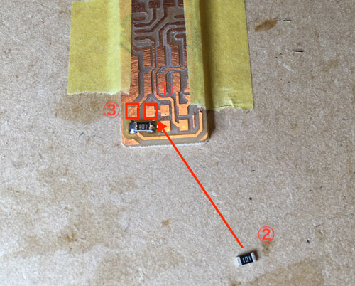
Tip
I recommend to solder only one side first before mounting the component. The only one side of component is fixed. And then, arrange the height because it might float it a little bit. then solder another side.
①Solder one side before mounting a component.
②Solder it at one side.
③Solder another side.
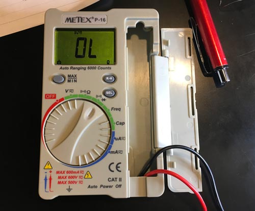
Checking conduction
Confirm whether all the pins are conducted properly one by one using the multimeter.
I set the alarm mode which ring the alarm when between two pins or points are conducted.
Finished
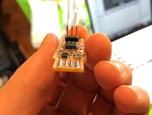
*Make sure to bridge J1 part by soldering to program using a programmer although in the above photo I forgot to bridge J1…
My thoughts
I have a chance to solder something on PCB in my work. So relatively easy to solder it. But I’ve not designed the pattern of PCB so I feel a little bit nervous with Electronics Design week…
3. Programming
Programming to my programmer
This captor, I think that’s the most complex and difficult part in this week.
What I did is that program the programmer using a programmer to write the program to the device.
Refer to the tutorial/Software Installation. But actually, I don’t understand this process perfectly.
① Download Crosspack form here.
② Download AVR assembler from Homebrew.
Terminal command of downloading AVR through Homebrew.
$ brew install avra
Issues
Some of the students in Kamakura installed AVR assembler directly form homepage. But by doing so, that didn’t work somewhat. We tried to solve this problem. But the solution was only download it using Homebrew and nobody can understand why we can success.
③ Download firmware source code from here. Click Download button.
Put the downloaded folder in the directory you like.
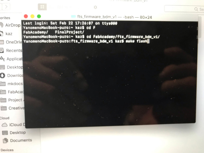
④ Open terminal
and go to the directory in fts_firmware_bdm_v1 folder downloaded at ③ on terminal and run make.
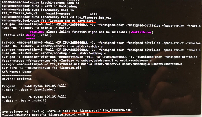
fts_firmware.hex file were made in fts_firmware_bdm_v1 folder.
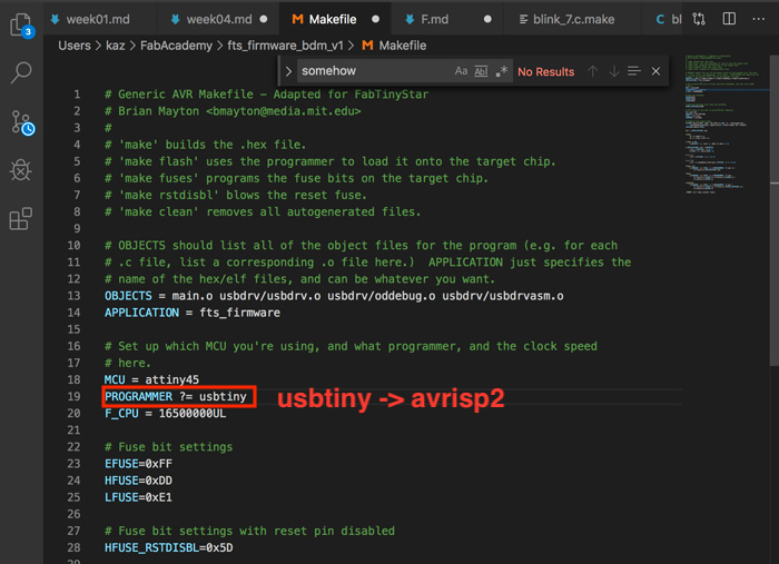
⑤ Open Makefile in fts_firmware_bdm_v1 folder using a text editor.
I used a small translucent blue programmer.
So edit PROGRAMMER ?= usbtiny to PROGRAMMER ?= avrisp2 according to tutorial.
⑥ Connect programmer to programmer
Again. What I did is that program the programmer using a programmer to write the program to the device.
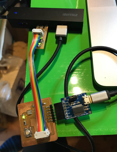
So connect my programmer to the blue programmer like the below image.
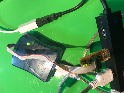
⑦ Program to my programmer
Move to terminal and then run make flash so that my programmer can program to other devices.
Uhh…
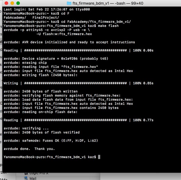
Congratulation!! I did it!!
Test the USB Functionality
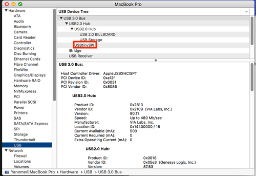
I inserted my programmer to USB port to confirm whether it is recognized as USB connection.
I use Macbook pro, Sierra version 10.13.6. So I confirmed the USB functionality from Apple Menu -> About this Mac -> System Report.
Note
At this timing, My programmer cannot be recognized when I proceeded in the order to tutorial. So I proceeded on Blow the Reset Fuse first.
First, open terminal and move to the directory in fts_firmware_bdm_v1 folder folder.
Then, after reading the below warning, run make rstdisbl.
Warning
Make sure that all the above processes are already done before running make rstdisbl. make rstdisbl command means that it will turn the ATtiny45’s reset pin into a GPIO pin. This will disable our ability to reprogram this ATtiny45 in the future.
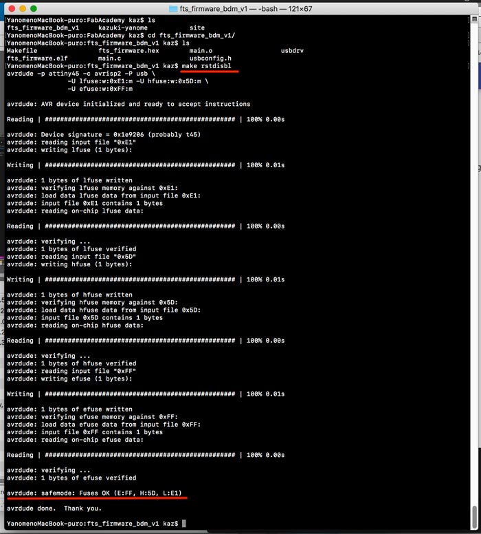
Remove my programmer from connection.
De-solder J1 part. Finished Blow the Reset Fuse.
Finally, connect my programmer to my PC again.
My programmer could be recognized properly~!!
Test Your Programmer
To test that my programmer can program the other device, I tried programming the PCB with LED using my programmer. The program that I used is that LED is turned on when I push the switch button on PCB, which can be downloaded form Jun Kawahara‘s week9 in 2018 page -> file chapter. And to work LED according to that program, I use the code described at Kae Nagano‘s week7 in 2019 page -> program chapter (Thank you all for providing tips).
Set up my programmer and test PCB like the image.
Download the folder from Jun Kawahara‘s page and put it at the same directory which has my mkdocs site page.
Go to its folder’s directory and run the below code.
$ make -f [Name of Makefile].make
$ sudo make -f [Name of Makefile].make program-usbtiny-fuses
$ sudo make -f [Name of Makefile].make program-usbtiny
Well done! Complete!!
My thoughts
Actually, I couldn’t understand what the codes I used means, how the programmer works completely this week. So I’ll take a memo about what I couldn’t unserstand so that I learn them later.
4. Conclusions
Submission
None
Self-reviews
1. This week’s work
All I did this week was my first time, so I learned them one by one. People in Fablab Kamakura member taught me how to do that even the students the same with me (Thank you.) Actually, I want to teach someone but I have enough knowledge now. So I need to learn more harder. With a high motivation, I”ll do my best!!
- Swap Debugging
This week, many students faced bugs at programming process though I passed it with somewhat a little problems. I’d like to support them but I didn’t know how I help them. Hideo Oguri who is one of the students in Fab Academy 2020 told me “Swap Debugging is the debugging way that I always use.” (Thank you.) Swap debugging is the way that you focus on two points and test them while swapping them. I learned about it and if I face bugs next time, I’d like to try that!!
2. Project Management
Score (Max: 100)
*I proceeded only tutorial this week. So my schedule was already managed.
-
Hierarchy: ?
-
Triage: ?
-
Spiral Development: 50
Only one spiral I did. -
Supply-side Time Management: 20
The time I scheduled in advance was expanded. I was doing literally Demand-side Time management this week… -
Parallel Development: ?
-
Document as you work: 60
Sometimes I forgot to take a documentation during the work…
MEMO
What I wanted to learn more
-
Crosspack
-
Homebrew
What’s the benefit of using Homebrew to download something? -
firmware source code
-
Hex file
What’s hex file? -
Make file and
make command
What what? I can’t understand everything!! -
Fuses
What is Fuses in program means? -
Eagle