6. Electronics Design
W6.1 : Observe the operation of a micro board.
W6.2 : Redraw an echo hello-world board.
W6.3 : Add a button and an LED.
W6.4 : Check the design rules.
W6.5 : Fabricate the board
W6.6 : Simulate the boards operation.
6.1 : Observe the operation of a micro board
6.2 : Redraw an echo hello-world board
Use Eagle to design the hello.ftdi.44
Eagle is one of the most common programs to use in the electronics design industry. It may be used as a stand alone software or as a plugin. For this reason I wanted to familiarise myself to it.
I found that it was quite intuitive to use once the basics were understood. The two tutorials by Jeremy Blum.com listed below were the best way to get started. However there were some extra installations to do. The component libraries for the parts that we needed had to be downloaded and installed into the program.These had already been compiled as part of the course materials: Eagle Libraries Download
Eagle Tutorial 1 : Schematic Design
Eagle Tutorial 2 : PCB Board Layout
6.3 : Add a button and an LED.
Schematic Design
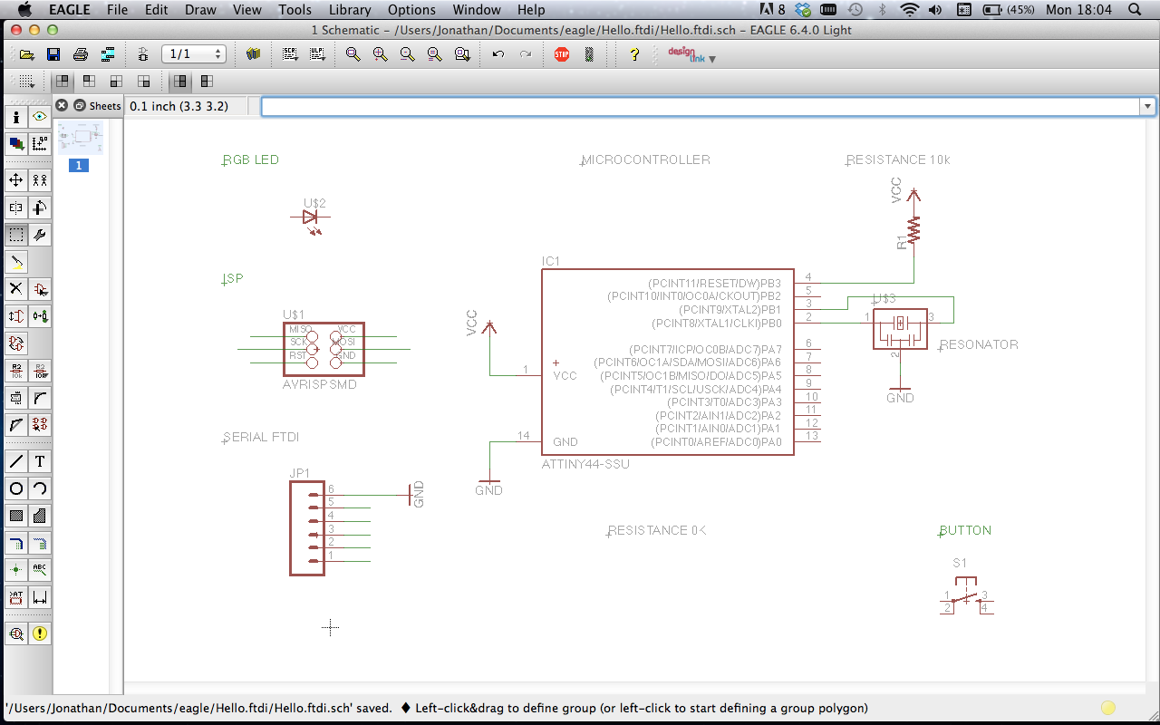
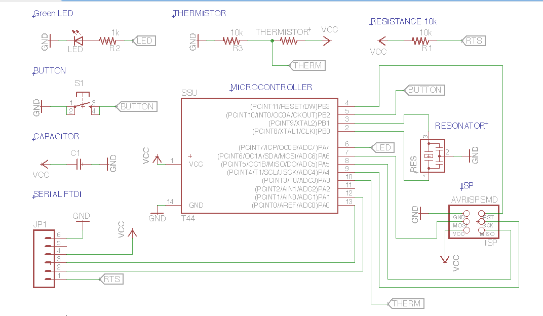
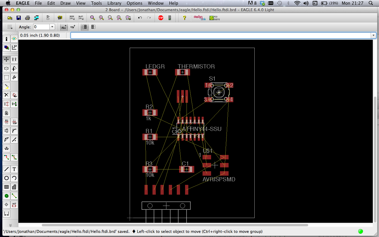
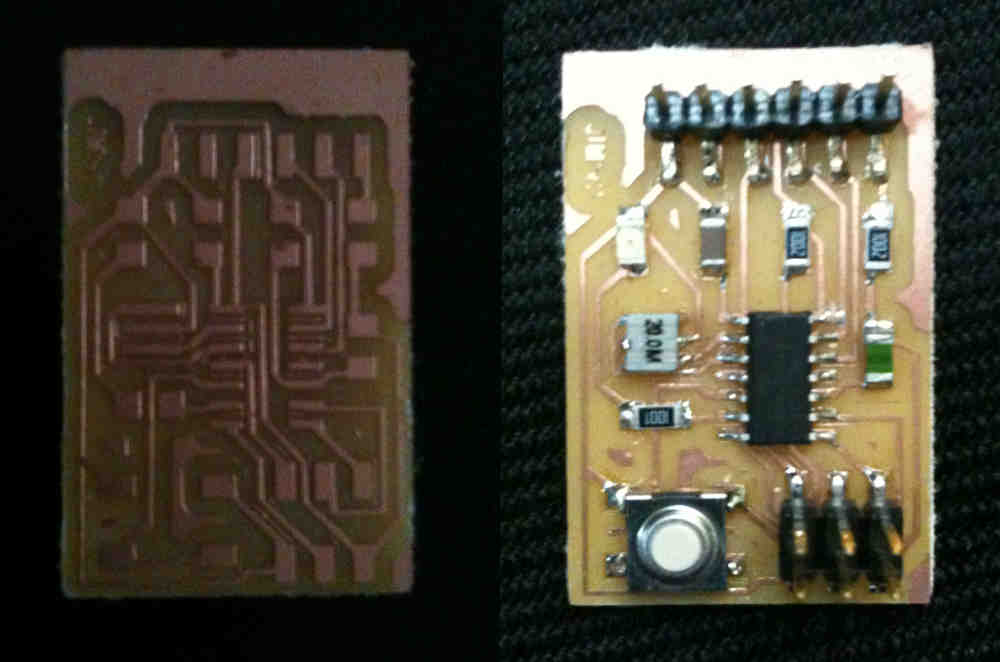
The academy class was to redraw and reconstruct the echo.hello-world board and to add both an LED and a Switch. I had been asked to include a sensor into the circuit also and that was to be a Thermistor to detect temperature for the joint Beehive project. The first task was then to select the correct components from the bill provided in part by the library and to begin to link them into the schematic.
Bill of components
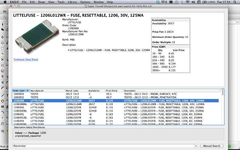
The component that I have used for this are listed in the diagrammatic to the left but are also available through the Design Link tool. I found this very helpful and a clear way to develop the parts list of the project. The Design Link and bill of components helped me greatly. In this way Eagle facilitates and synthesises real world components and CAD software. Once on the board the task of connecting the components was made easy by using the virtual tags method. Where multiples of connection points such as Ground (-) and VCC (+) are linked by tagging a word. Once the Schematic and Bill of components was complete it was time to move onto the board layout.
Board Layout and Ratsnest
A new board layout is generated and saved to the project folder by clicking Generate/Switch to board button on the top left of the Eagle screen. Anything in the refference pictures that has a black background comes from the Board view. We have been asked to use a single side PCB board for this project. This means that we can only use one layer to generate the Traces, otherwise we could have drilled holes or ‘Ground Pour through the board and connected Via’s to another side of copper PCB.This would have made it easier to avoid crossed wires, but harder to use the milling maching and to align both sides later. The ‘Ratsnest’ tool can be used to generate the shortest and most efficient paths between components before generating the final position and layout.
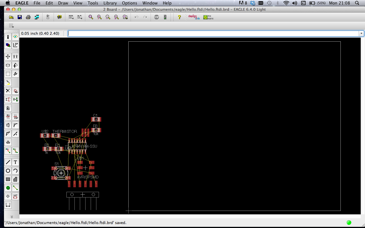
Auto / Manual Routing Vias
After creating the layout for the components the ‘Autorouter’ tool made arranging the Vias between components easy. The tool generates an automatic layout for these traces and can be refined by changing the grid from 50 to 30 points. Some final arrangement could be done using manually routing tool. Finally it is possible to use the ‘Smash’ or Info commands to resize and place the names of components onto the board. the boarder can also be moved to fit the trace layout snuggly.
6.4 : Check the design rules.
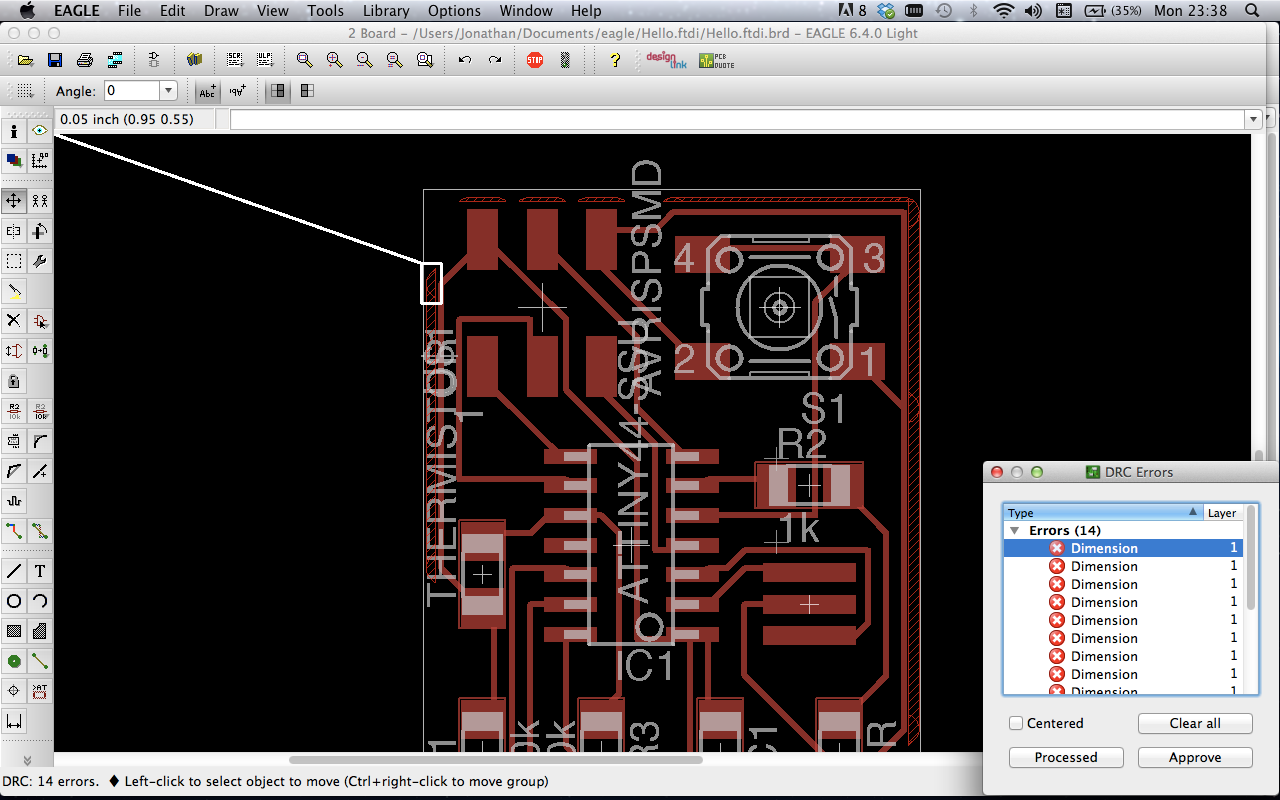
DRC = Design Rule Checking and Export
As a final step it was useful to use the DRC check to make sure that all Traces will work. This may produce many results. Many of these will be where the Litho print layer is superimposed over the traces. (This is not a big problem). Another rule is that there must be a sufficient gap between the last trace via and the boarder edge of the design. (This is a problem).
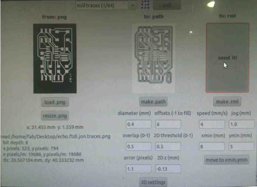
6.5 : Fabricate the board.
Repeat Production Process : Week 4
This process follows exactly what we have produced before. However there are some further notes and lessons learned:
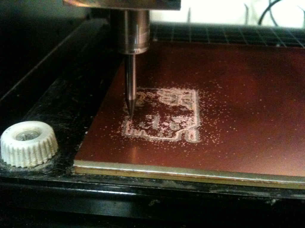
- The PCB Must be placed at a completely flat on the machine base, otherwise the cutting bit may miss the board. This can be solved by dropping the bit and redoing the trace again in a second pass.
- Make sure that the traces are not too small. a milling bit of 0.4 mm is ok.
- 1/64 milling bit and a offset 4 is sufficient for most jobs.
- I set my traces to be autorouted on a 30 point grid in the beginning. This proved to be too fine but worked ok with a new bit.
- Set the line width to be a larger width than 0.12 mm.
Next was to stuff the board with components.
Research
Key Resources
Code Example
- Need to add libraries from kicad github
- Need to link simbols