Assignment 6: Electronics Design

Project Description
Explore Electronics Design
Assignment Details
- Group Assignment:
- Use the test equipment in your lab to observe the operation of a microcontroller circuit board
- Individual assignment:
- Redraw the echo hello-world board, add (at least) a button and LED (with current-limiting resistor)
- Check the design rules, make it, and test it
- Extra credit: simulate its operation
- Extra credit: render it
I had some problems getting started this week. I downloaded KiCad and installed it on my Mac. Brought up the Symbol Library Editor, typed text into the search bar and the application crashed. Brought up the schema editor, clicked on Place a Symbol, typed some text in the search field and the app crashed.
I needed to make progress on the assignment, so I fell back to my old PC. I downloaded and installed the PC version of the software. Next I went in search of training. My normal source of training lynda.com had nothing for KiCad. Next step was to fall back to generic YouTube videos. I found a series sponsored by DigiKey that stepped through creation of a through the hole electronic badge An Intro to KiCad. These videos served as my base of knowledge. The videos were for version 4 of KiCad and I downloaded version 5, but I hoped that it would be close enough to what I needed. I watched the first video and it talked about how to create a new schema symbol for a 555 timer and how to add missing schema and footprint components. I haven’t spent a lot of time in Electronic CAD tools, but the ones that I have used came out of the box with most everything that I needed, so I was happy that KiCad could be extended, but scared about the amount of work needed to make it usable. (Adding footprints, etc)
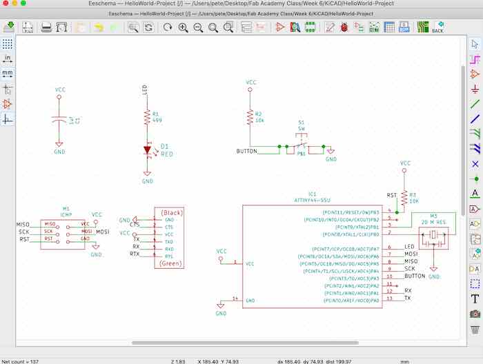
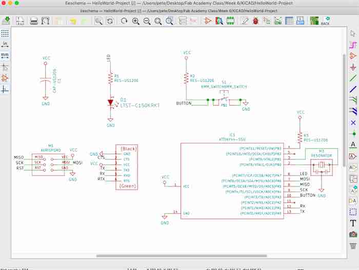
I have some background in electronics, so I knew conceptually what would be needed to build a schema with pull down resistors for the switch and a resistor in series with the LED. Because this was intended to be a “Hello World” example, I went in search of some project specific instructions. I found the class Tutorials for Week 6 section covering Eagle. Even though I was not using Eagle, I decided to use it as a model for my project. The introduction to Eagle section contained a sample schema and a description of the steps needed to complete the project. I used this as the template for what I did in KiCad.
I built the schema using KiCad on the PC. On the next day I checked back with the KiCad download site and found that a new version of KiCad had been released for the Mac. I downloaded this version and redid the schema and completed the rest of the assignment on the Mac.
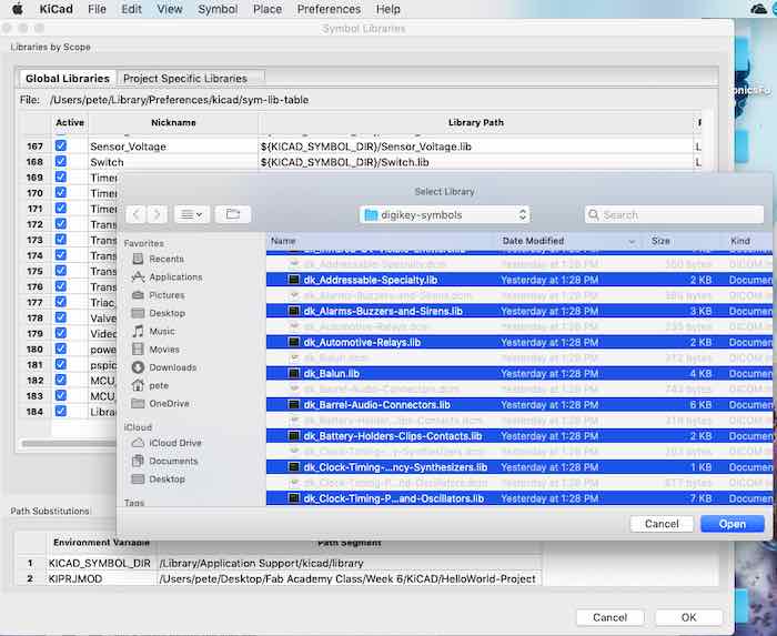
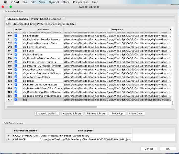
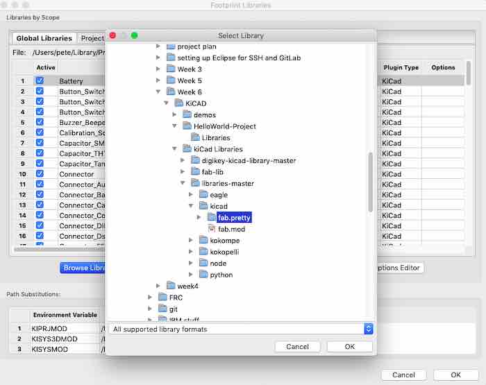
Of course when I tried to add the symbols that were identified in the tutorial, none were found in the library. I created a new library folder to hold both my local and global libraries. Next I went in search of KiCad libraries. First I found the DigiKey library and added it to KiCad. Later I found the Fab Academy site with the KiCad schema and footprint components. This made me feel a lot better about KiCad.
The next step was to build the schema using the Schema Layout Editor. It was recommended to update the drawing preferences with author name, version, and date information. This helps to keep the fabricated board in sync with the version of the associated schema.
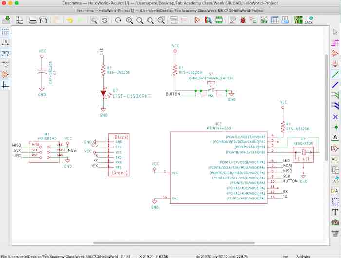
The next step was to add the component symbols to the schema.
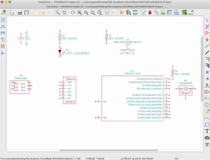
The next step was to add the labels.
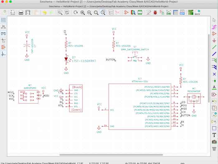
The next step was to connect the components using lines.
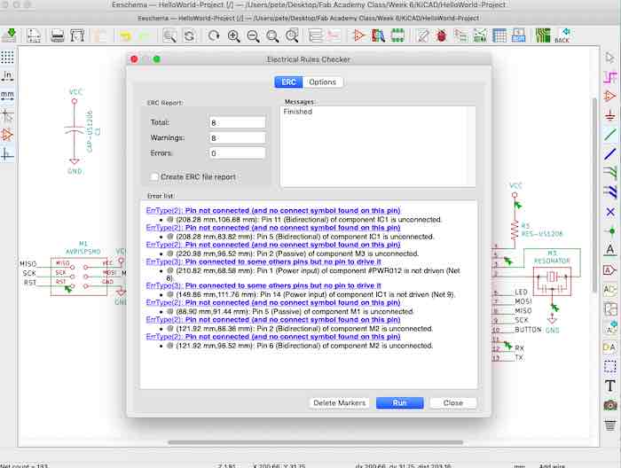
Running the design rules check identified some warning but no errors. I found a missing connection and corrected it.
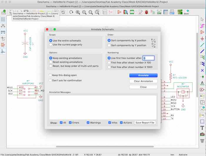
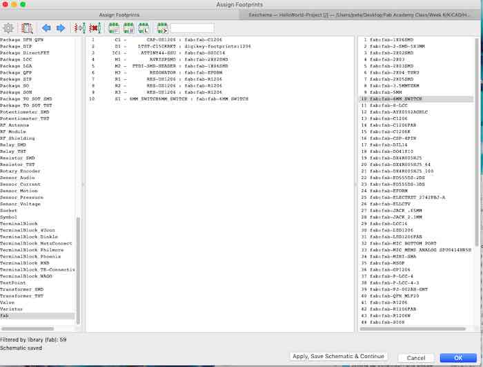
The next step was to annotate the symbols. Since this was the first time I was doing this, I left the default values. This assigned names for each of the components.
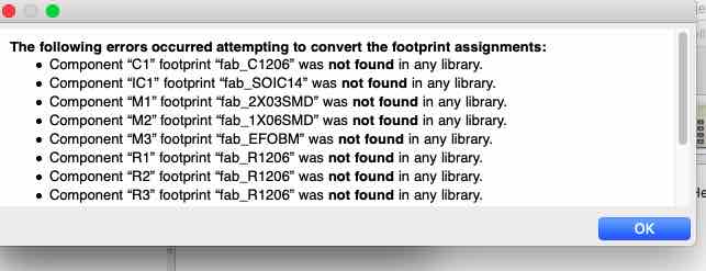
I ran “Assign PCB Footprints" to schematic symbols and encountered this error. This was due to the footprint library for the fab parts not being added to the libraries. The next step was to add these libraries and rerun the command. This didn’t correct the problem. I had to go into the mapping editor and reassign the footprints for each of the individual components.
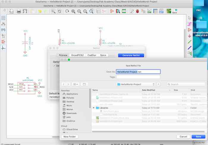
Next, the NetList was saved from the schema editor.
Next I opened PCB Editor and loaded the netlist and found some errors. I went back to the footprint mapping editor and fixed the mapping problems, created a new netlist, opened the PCB editor, loaded the netlist and then found that I forgot to add the component values to the parts in the schema. I went back and assigned the values, created a new netlist.
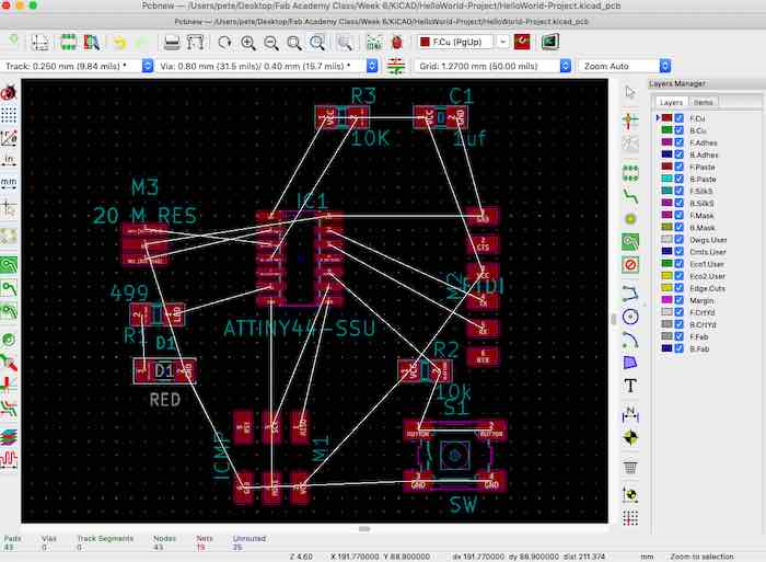
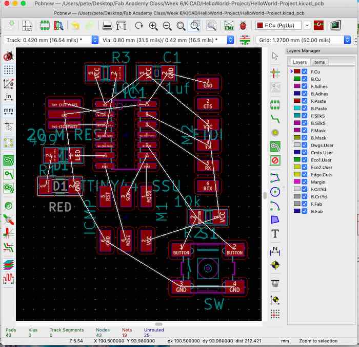
I opened the PCB editor and loaded the updated netlist and moved the components apart to get a general board layout.
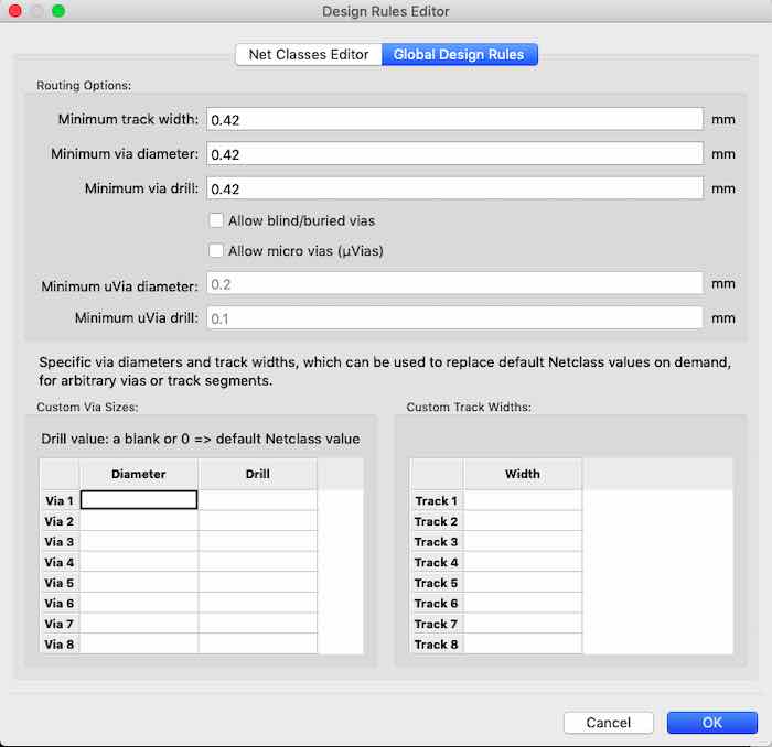
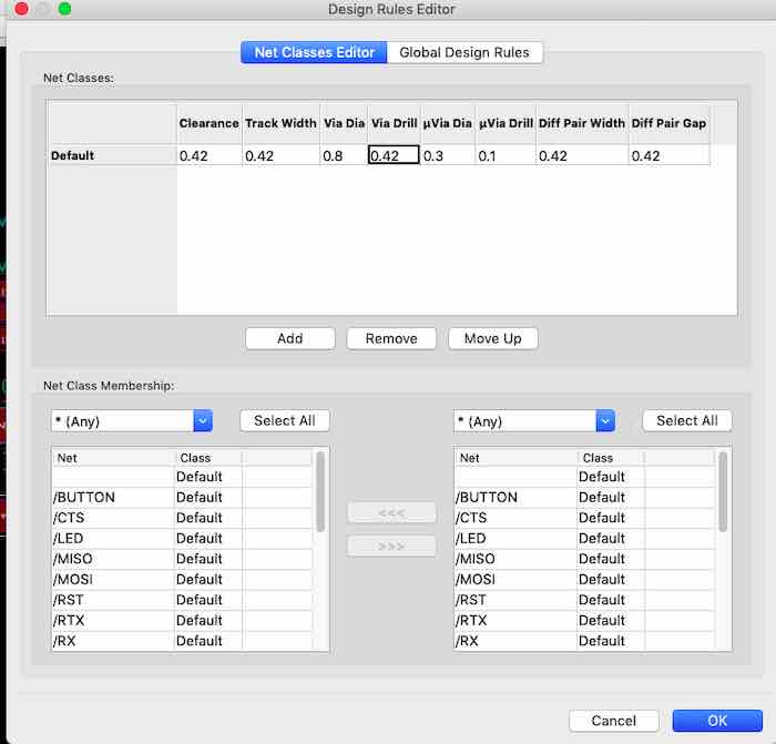
Next I changed the PCB design rules to set the minimum trace and spacing to 0.42mm. I didn’t change all the via dimensions, since this is a single layer board.
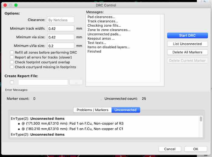
Next I executed the design rules. There were no problems but showed all the traces as unconnected. I updated the rules to match the end mills in my CNC.
Next I moved the components closer together leaving enough space for the traces.
I rechecked the PCB and noticed that I was missing a connect to the RST pads. I went back and added the missed the RST label on the schema view.
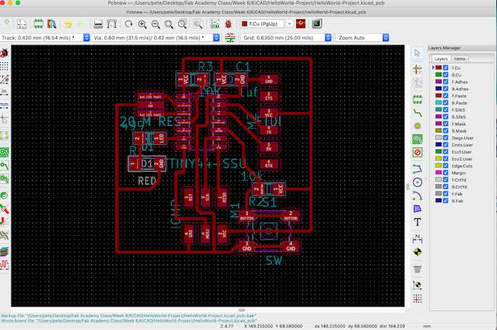
Recreated the netlist, opened the PCB editor and loaded the netlist to create the final PCB design.
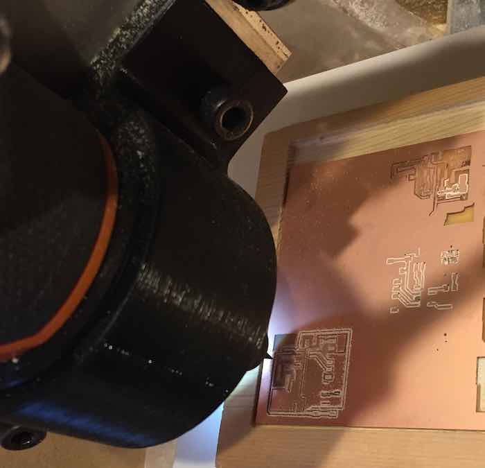
KiCad creates a SVG, but the inverse of what is needed to cut on my CNC. I had to go through a series of steps to generate the svg for what was needed to be cut. First, I exported the SVG and opened it in Inkscape. I exported the SVG as a PNG. I opened it again in Inkscape and ran an inverted create path from bitmap to create the final SVG for cutting everything but the traces and pads. I imported the inverted cut SVG into Easel and generated g-code for the PCB with a 0.3mm cut depth. I zeroed the z axis but found that the bit didn’t cut. This was likely due to the spoilboard surface not being perfectly flat. I resurfaced the spoilboard, reapplied the double stick tape and applied the pcb material to the spoilboard and reexecuted the PCB G-Code.
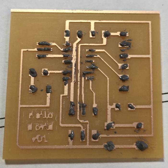
Here is picture of the milled PCB.
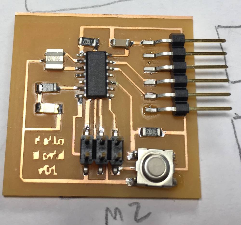
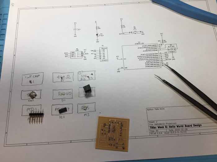
Here are the parts components organized and the board coated with flux.
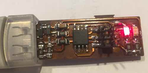
Here is "hero" shot of the finshed PCB.
I understand that the "group" project was to use the o'scope to debug the board. Before I hooked up power I did continuity checks to make sure that vcc and gnd checked across the board. I also validated that there were not any shorts. At this point, I decided to first see if the board worked before I started more in depth debugging. (Why fix a non-existent problem? - Turns out the board worked on the first try!) It took some time to figure out how to program the board and I realize that it overlaps a bit with a future assignment. Basically I used the Arduino IDE to push the bootloader which set the fuse to set the clock at 20mHz. Last I modified the example switch code with the revised button and led pins and pushed the code. (LED on, then off when switch pushed.) Just to validate that everything worked, I reversed the logic (LED off, then on when switch pushed) to validate that the changes were due to my activities. I am sure that I will have the opportunity to debug boards in the future.
Reference Files
Related Projects