Assignment 10: Input Devices
Project Description
Explore Input Devices
Assignment Details
- Group Assignment:
- Probe an input device's analog levels and digital signals
- Individual assignment:
- Measure something: add a sensor to a microcontroller board that you have designed and read it

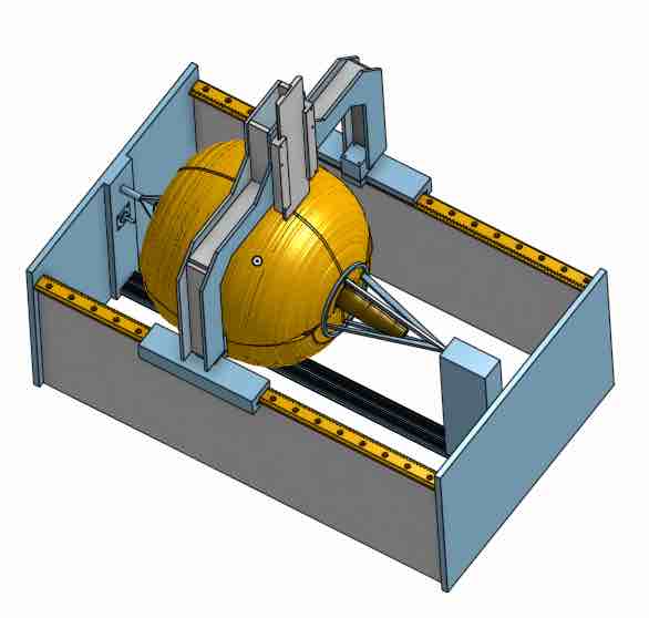
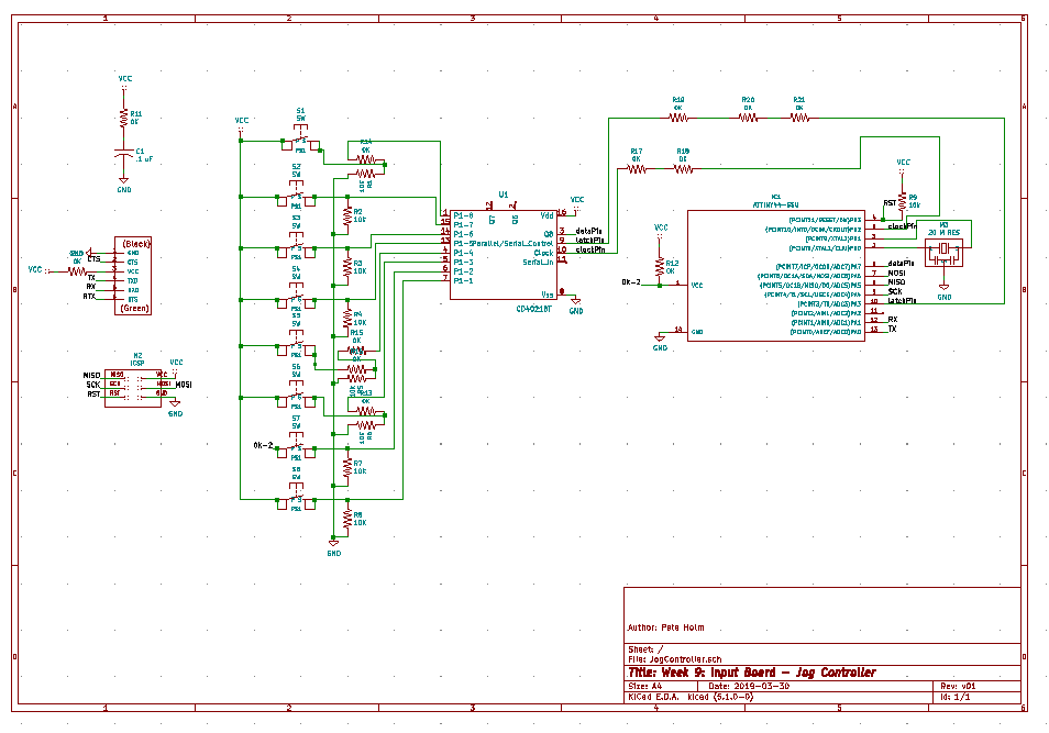
This week's project adds to the work done in last week's project to mold a Jog Controller for my final project, a Pumpkin CNC. The figure above shows the interaction flow from the Jog Controller to the Pumpkin CNC. The Jog controller reads button inputs from the user to move the mill, play or stop g-code files. These inputs are read by the ATTiny 44 and communicated to a Python script using the serial I/O channel. The Python script maps the button press to an associated Universal G-Code Sender (UGS) command. The command and associated parameters are send to the UGS REST Server via a POST command. UGS, then sends the G-Code command to the board running GRBL. Finally the GRBL board translates the G-Code commands to stepper motor signals which move the mill. The goal of this week's works was to create a PCB with switches to start the command flow described above.
This week's assignment has been challenging. Each step of the way there were issues and road blocks that needed to be solved. I got through most of them and am working to resolve the last issue.
Issue 1: More inputs than data lines on the AT Tiny44
The easy way to do I/O on AT Tiny boards is to dedicate an I/O pin to read input values. The AT Tiny doesn't have 9 data pins, so this approach will not work. I have needs for 9 buttons that control:
- + / - X Axis Movement
- + / - Z Axis Movement
- + / - A Axis Rotation
- Play (Execute) G-Code File
- Stop G-Code File
- Pause G-Code File
Alternative Solutions for Issue 1: Lack of I/O lines
Initially, I started down the path to look at a trick using Diodes called "Charleyplexing". Charleyplexing has been described in this quote:
“The more straightforward method uses N I/O lines to scan and decode a matrix of (N/2)2 keypad switches. Half of the lines are used for input and half are used for output. For example, row scan lines are set as inputs, and column lines are alternately driven as outputs. The new method uses all lines as both input and output. In this way N I/O lines are capable of detecting up to N2-N switch closures.”
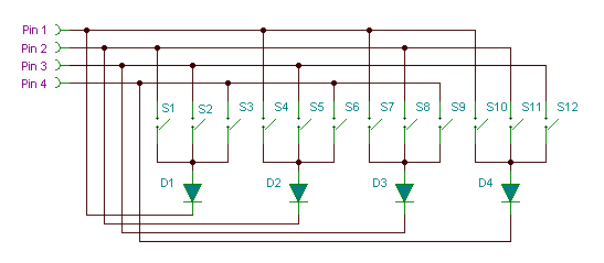
This technique uses the fact that any AT Tiny data line can be Input, Output, or High Impediance. The software cycles through combinations of these states on each data line to determine the state of each switch.
This technique has some problems. First it assumes that only one button is pressed at a time and it suffers from "ghosting" (detecting switches that are not pressed), in some cases.
Because of these problems concern about CNC safety, I decided to continue searching for other techniques.
After more exploration, I remembered back to the old days of printers. Older printers could be divided into 2 types: Serial and Parallel. Parallel printers had wire cables that transmitted many bits at the same time to be read in one operation. Parallel printers had simpler cables that conceptually transmitted one bit at a time. A IC called a shift register was used to convert from parallel to serial to serial to parallel. In my case, going from parallel to serial would give me what I needed and it supported having multiple keys pressed at the same time.
After some research, I found an IC that provided an async parallel input and a synchronous serial output. It required just 3 I/O pins and could support input 8 bits for each chip. Chips could be chained together to get more than 8 inputs.
Here is the data sheet for the Data sheet for CD4021B - CMOS 8-Stage Static Shift RegisterNext, I went in search of any previous examples using this chip and an Arduino. I found this example Parallel to Serial Shifting-In with a CD4021BE. The next step was to build a schematic for the circuit. I rapidly discovered that there were no existing symbols or footprints for this IC supported in KiCAD. The next step was to use the Symbol editor in KiCAD to create one.
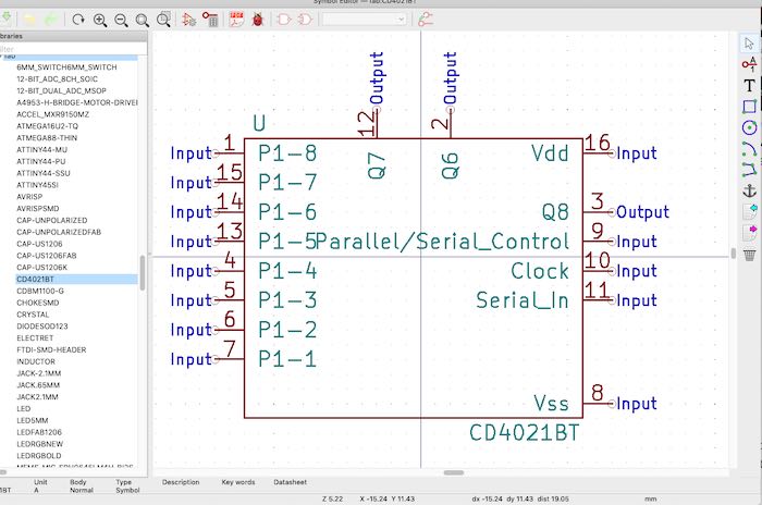
After adding the symbol I was able to create a circuit using our AT Tiny 44. Each switch is connected to a parallel pin on the CD4021B. The line is pulled low with a 10K resistor. Pressing the button pulls the line high and sets the bit on the CD4021B. The serial side is controlled by three pins. The clock, data and latch pins connect to the data lines on the AT Tiny. Pin 9, parallel serial control, is used to chain multiple chips to support more than 8 inputs.
To validate that the IC worked with switches the way that I expected, I built a quick prototype on a breadboard.
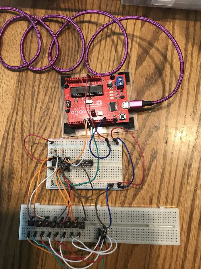
This video demonstrates reading key presses as an 8 bit word. I have a serial console open on the output from the board. The screen shows a binary word with any pressed switches shown with a 1 in the associated bit position. I also bit masked the input to display a letter assocated with the key. If more than one key was pressed, then multiple 1's appeared in the word and multiple letters. (Leading zeros were not shown in the output).
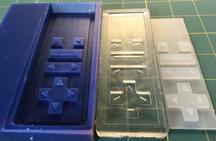
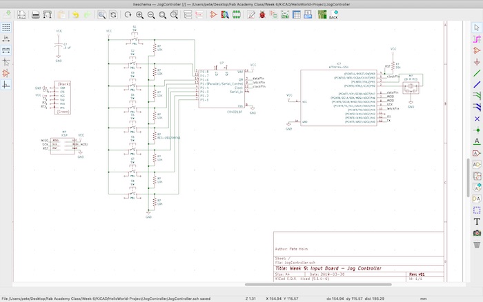
The next step was to design the circuit board. This was more complicated than the "hello world" board, because the switches had to line up with the pads from last weeks's casting and the entire board needed to fit in the remote FOB packaging.
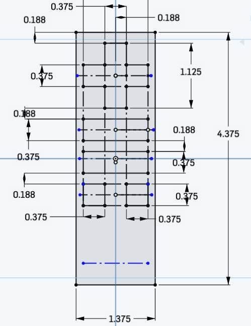
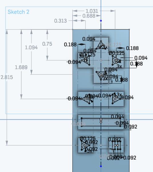
The first figure shows the overall dimensions and the second specifies where the buttons need to be located.
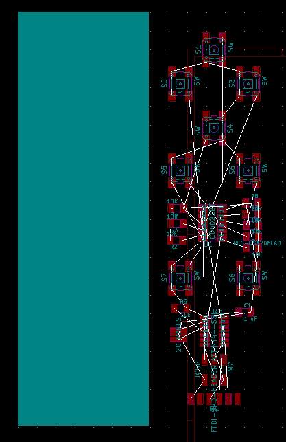
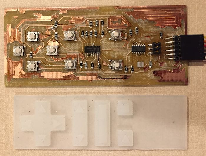
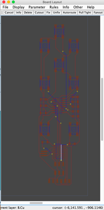
The figure shows the resulting layout of the PCB with buttons located under the Jog Controller pads. The traces have not been routed, so appear to be a bit of a "rats nest".
Issue 2: Routing traces given the required location of the switches
I banged my head against the wall trying to route all the traces for most of a day. While for some this could be considered "a game", for me it was an exercise in frustration. To resolve this problem, I considered moving from KiCAD to Eagle. Given the shrinking available time, I decided to stay with KiCAD and look for an auto router.
Solution for Issue 2: Routing Traces
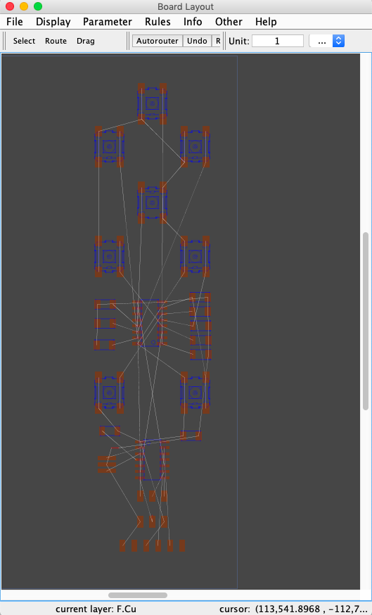
After some research, I found that other E-CAD programs use a tool called Free Router. The recommendation to get Free Router was as part of another tool called Layout Editor. The example showed how to get to the Free Router .jar file within the Linux version of another application called Layout Editor. I am on a Mac, so of course this didn't work. I drilled into the Mac application and found the .jar file, but when executed the .jar file, did not provide the UI prompt to open a Specctra DSN file. After another day of research, I found the GitHub site for FreeRouter and downloaded the .jar file. This new file appeared to work with the file exported from KiCad.
I felt better when it took some time for the auto router to figure out a solution. My happiness was short lived.
I imported the Spectrum session file back into KiCAD and discovered a new surprise.
Issue 3: The auto router generated a solution based on a 2 sided board with Via's
I thought about buying a new batch of double sided blank boards and trying out 2 sided milling. I also considered including a pad or through the board holes and solder connecting wires. This consumed another day looking at this problem.
Solution for Issue 3: How to mill a single sided board from a routing with via's
When I made my order to Digikey for electronics components, my mentor recommended that I also include some 0 Ohm resistors. After some thinking, this appeared to be the application for these components.
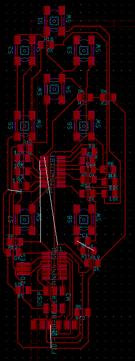
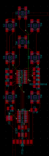
I went back and revised the design to replace each via with a set of 0 Ohm resistors which went over the other traces. This led to a revised design which could be milled on a single sided PCB blank.
At this point, I thought that my problems were all solved and that I was on the home stretch for finishing the assignment. Wishful thinking.
Issue 4: The bracket holding my router on the CNC broke
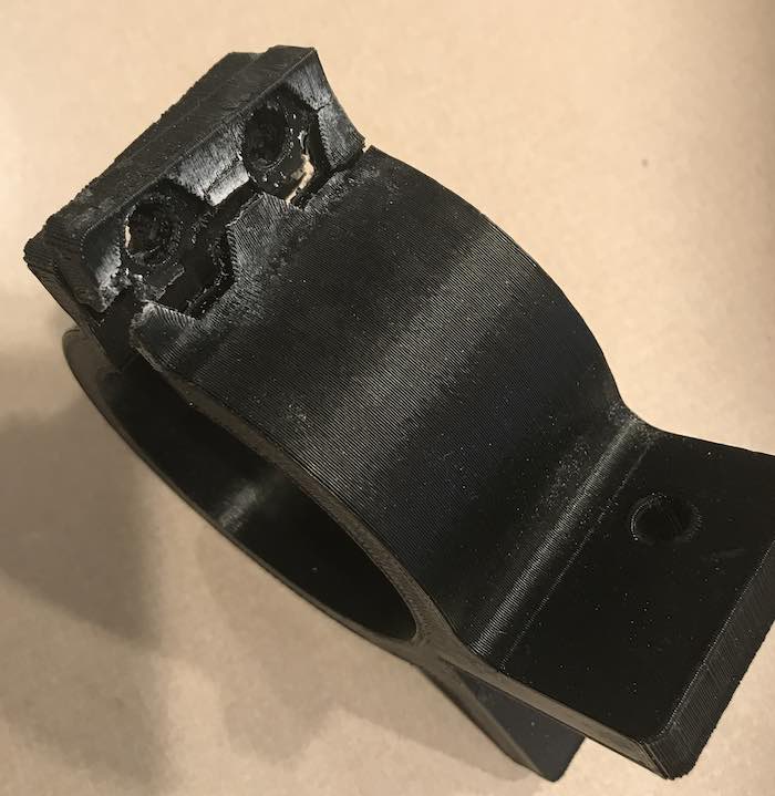
Solution for Issue 4: 3D Print a new bracket
I made an attempt to glue the part back together. As expected, the fix did not work. I fell back to the solution of creating a replacement part. I downloaded the STL file, sliced the file and started the printer. After a couple of incomplete prints and 2 days of elapsed time, I got a finished 3D print. The next step was to mill the board.
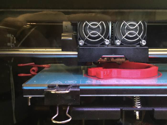
Issue 5: CNC not successfully milling the PCBs
I milled a new pocket in the soil board for a parallel surface. The pocket was slightly larger than the board but I thought that the double sided tape would hold the PCB in place. About 3/4 of the way through the job, I notieced that the board was moving on the X axis when the router moved back and forth. I tried to insert a shim between the PCB and the edge of the pocket. While this may have reduced the movement, it ultimately didn't solve the problem. I ended up starting with a new piece of spoil board and milling a slot exactly the size of the PCB and trying again.
The picture above shows some of my many failed attempts to mill this PCB. I am not sure what changed between the time that I was successful with creating PCBs and now. I ordered new 1/64 end mills and will try again when they arrive.
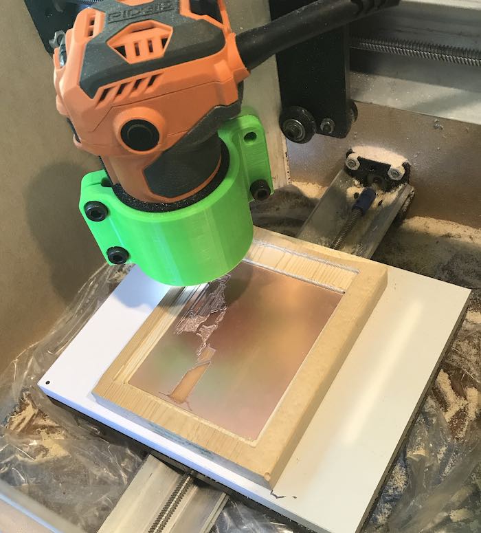
Solution for Issue 5: Milling PCBs
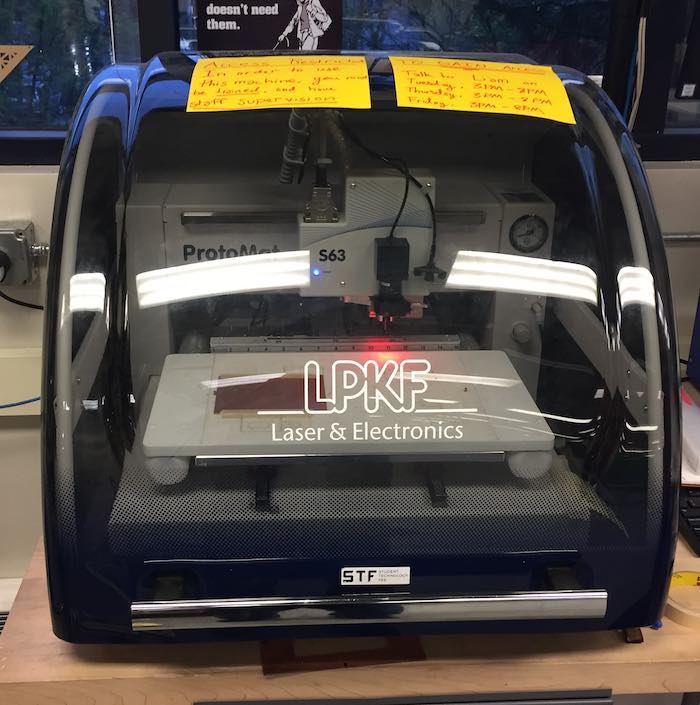
I joined the University of Washington's Co-Motion Makerspace. The picture above shows their PCB mill. It still has issues with milling open space, but it cut traces with enough room that there was no bridging.
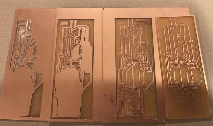
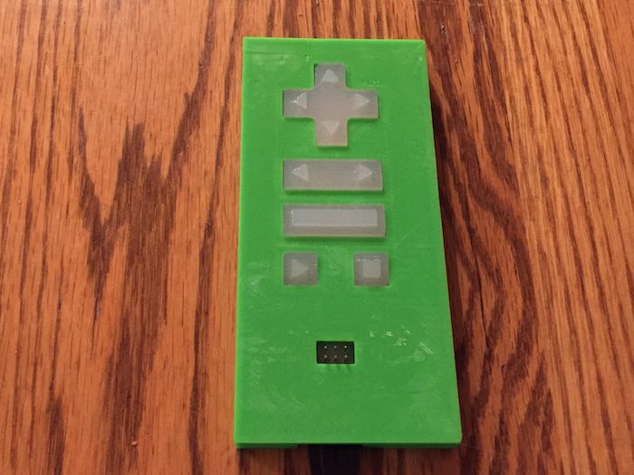
The figure above shows the completed PCB after it came out of the reflow oven. The switches are arranged to up under the pads from the molding and casting assignment.
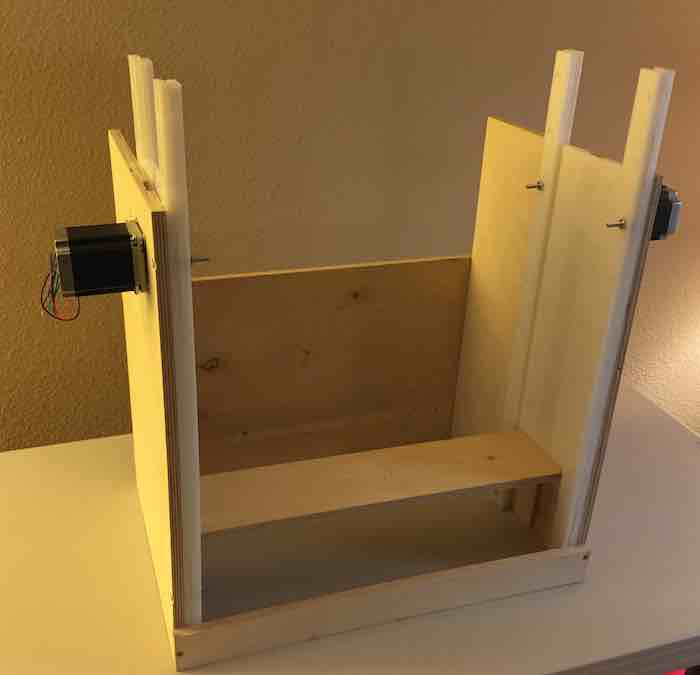
The following figure shows the finished Jog Controller Assembly
The Arduino code is basically the same as what was used on the breadboard, except the pin numbers are adjusted for the ATtiny44. The shift register is based on 3 pins: latchPin, clockPin, and dataPin. The protocol is to set the latchPin high to read data into the parallel registers. Then the latchPin is pulled low and then the clockPin is set as an output and the dataPin is set as an input. Next the clockPin is pulled low and the dataPin is read. This cycle is repeated 8 times (once for each parallel pin). This results in a byte of data. The position in the byte represents the switch which is pushed. If more than one button is pressed, more then one bit will be set. The test program returns a direction that maps to the pin that was pushed. This is sent over the serial connection back to the terminal program. The terminal program will eventually be replaced with a Python program that makes a REST call to Universal G Code Sender to control the CNC Lathe.
The next video clip shows a demo of pressing a button and the result being displayed on the screen. This demonstrates the right side of the flow diagram at the top of the assignment. The rest will be programmed in the application programming week.
Reference Files
Related Projects