11. Input devices
Week 11: My head is spinning and I am a nervous wreck! This week we are tasked with designing a controller board and programming it to receive and process input signals. All of this is beyond my current knowledge. What to do…?
“Failure IS an option…” Do, fail, learn…repeat this ‘While Loop’ (is this good that I am making jokes with programming commands??) until understanding and success is achieved. Deep breath…here I go.
The Group Assignment page here
Assignment Requirements:
- Design and fabricate a controller board from scratch that includes one or more sensors
- Write a program to process and input signals from the sensor
- Upload and test the program on the board
Being certain to… - Describe the microcontroller/sensor board design and fabrication process - Describe the programming process and how the microcontroller datasheet helped - Explain problems encountered and how it was fixed - Include original design files and code
The Plan
For my final project, I anticipate the use of the following sensors…
- Accelerometer…recognize when the brakes on a motorcycle are applied
- Gyroscope…recognize when the rider leans forward or sits upright
- Photo Transistor…recognize light and dark riding conditions And also possibly…
- Temperature & Humidity…recognize when it is foggy or raining
For this week’s assignment, I planned to work with the Accelerometer and Gyroscope but ended up working with the Accelerometer and Phototransistor.
- Sensor Research: Understand the Accelerometer and Gyro
- Board Design: figure out how to design a board incorporating these sensors…(prototyping it using an Arduino and a breadboard first?)
- Board Fabrication: design & fabricate (mill & stuff)
- Coding: use and figure out how to modify (if necessary) code presented by Neil during the lecture…to utilize the sensor
- Board Programming & Testing: upload the program to the board and test its functionality
Pre-Work Session Preparation
Research: The Accelerometer & Gyro sensor
First steps, understanding the sensors…
Afrotechmods: How an Accelerometer Works!
The Afrotechmods video here
Learning Outcome:
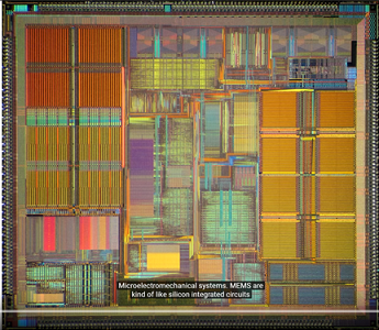
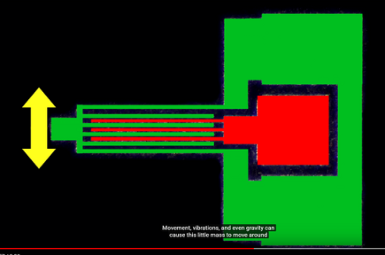
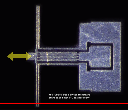
Micro-Electro-Mechanical-Systems (MEMS) - Mechanical switches at a microscope size.
MEMS Capacitor - Micro-size capacitor. - Movement allows separated conductive plates (in a ‘Combed Finger’ arrangement) to move closer or further away from each other…changing capacitance levels.
MEMS Accelerometer - More combed fingers than a MEMS capacitor.
Michael Schoeffler, Tutorial: Gyroscope and Accelerometer (GY-521/MPU6050) with Arduino
The video here
Learning Outcome:
GY-521 Overview The GY-521…is a break out board built around a MPU6050** chip that contains many on-board sensors/functions including…
- 3-axis Gyroscope: uses earth’s gravity to determine orientation
- 3-axis Accelerometer: measures non-gravitational acceleration
- Temperature sensor: measures ambient temperature
- Digital Motion Processor (DMP…can be used with ATTiny??): processes complex algorithm directly on the board; transforms raw values from sensors into stable position data
Pin Overview
8-pins:
-
VCC: voltage supply, with regulator to allow for 3.3v and 5.0v sources…wired to Arduino 5.0v pin
-
GND:…wired to Arduino GND pin.
-
SCL: Serial Clock, for I2C serial bus communication protocol…when GY-521 used as an ‘I2C Slave’…wired to Arduino’s A5 pin
-
SDA*: Serial Data, for I2C serial bus communication protocol…GY-521 typically an ‘I2C Slave’…wired to Arduino’s A4 pin
-
XDA: Auxilliary Data, for I2C serial bus communication protocol…when the GY-521 used as an ‘I2C Master’…reading data from other sensors without intervention from main processor
-
XCL: Auxilliary Clock, for I2C serial bus communication protocol…when the GY-521 used as an ‘I2C Master’
-
ADO: If LOW, address is 0x68, if HIGH is 0x69
-
INT: Pin used to handle interrupts
Code for use with Arduino
- Arduino Wire library for I2C communication.
- Reading 7 sensor values…3 Accelerometer, 3 Gyroscope, and 1 temperature values
- Values stored on MPU6050 registers…starts at 0x3B for the 1st X-axis Accelerometer value, with subsequent values stored in the next registers in series.
- 14 registers need to be read…as each value requires 2 registers each.
- The 2 registers for each value are read and combined. Bit-shifting used to assign HIGH byte to the first register and LOW to the second register.
- Advanced MPU6050 library…I2Cdevlib available here
Datasheet Learnings - Accelerometer
The ADXL343 datasheet can be viewed here
- The ADXL343 is an Accelerometer chip produced by Analog Systems
- The chip measures ‘Acceleration’ in 3-Axis
- I intend to measure ‘Deceleration’ to activate my Brake Light program
- Because it measures in 3 axis, I hope to use the sensor to measure the rider body position as well…inferring body orientation from relative axis acceleration data
- A reasonably high resolution sensor with 10-13 bit resolution
- More than I will need, as I intend to measure large, infrequent movements…not constant, small movements
- Communicates with both I2C and SPI communication protocols
- I plan to use I2C
- Embedded FIFO allows for low power consumption
- My device will be on battery power and low power consumption when inactive is a big plus
- Accepts voltages between 2.0v and 3.6v
- I will need to regulate the 5v sytem power down to 3.0v
- The Accelerometer has a robust set of ‘Interrupt’ functions…and 2 interrupt pins configured as ‘Active High’. Amazingly, the datasheet states that all functions can be used simultaneously…and functions can share interrupt pins. Triggering the HIGH state is via bit setting in the INT_ENABLE register (address 0x2E), mapped to either pins via INT_MAP register (address 0x2F). Configuring interrupts requires disabling/clearing the bit in the interrupt registers first with the INT_ENABLE command.
- I intend to use one to trigger the Brake Light function and another to measure rider lean angle and activate device ‘wing’ position changes
- I will likely utilize the DATA_READY (where new data availability sets a bit) and THRESH_ACT registers (where the activity bit is set when acceleration…or deceleration in my case…is greater than a store threshold level)
Work Session: Day 1
Board Design
Board design proved to be a day long ego-crushing ordeal. Left the lab 12 and a half hours after arriving with nothing to show but routing in Eagle. Defeated.
The Synopsis of the Drama…
1. I deviated too far from Neil’s lesson plan…trying to work with a breakout board rather than just recreate one of the boards he suggested (when my knowledge on electronics is near zero)
2. When I gave up and decided to build Neil’s board…I made many mistakes that resulted in a non-functional board
Act 1
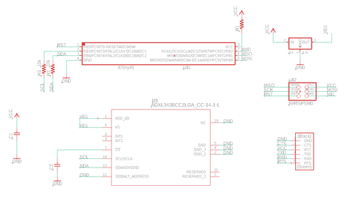
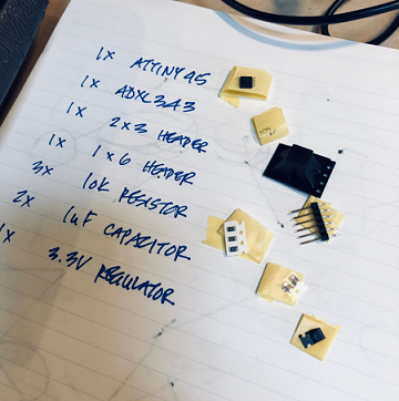
Initially planned to build a board with both an Accelerometer and Gyroscope sensors soldered on to it (along with the microcontroller)…as they are two critical sensors for my proposed final project. Out lab had a standalone Accelerometer SMD sensor (the Analog Device ADXL343) but no Gyroscope. What we had was a GY-521 breakout board with an MPU6050 chip that contained both Accelerometer and Gyroscope sensors.
The plan was to design a board that…
- Used an ATTiny44 microcontroller (so I can expand on the datasheet work I did the previous week)
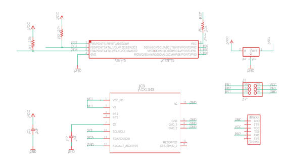
- Had a FTDI connector for power and serial communication with a PC
- Had an ISP connector to allow for programming via a FabTinyISP
- Had a 8-pin connector to allow the GY-521 board to be connected to the board
- …had a 10k Resister and a 1uF Capacitor (…which I assumed was needed by the ATTiny)
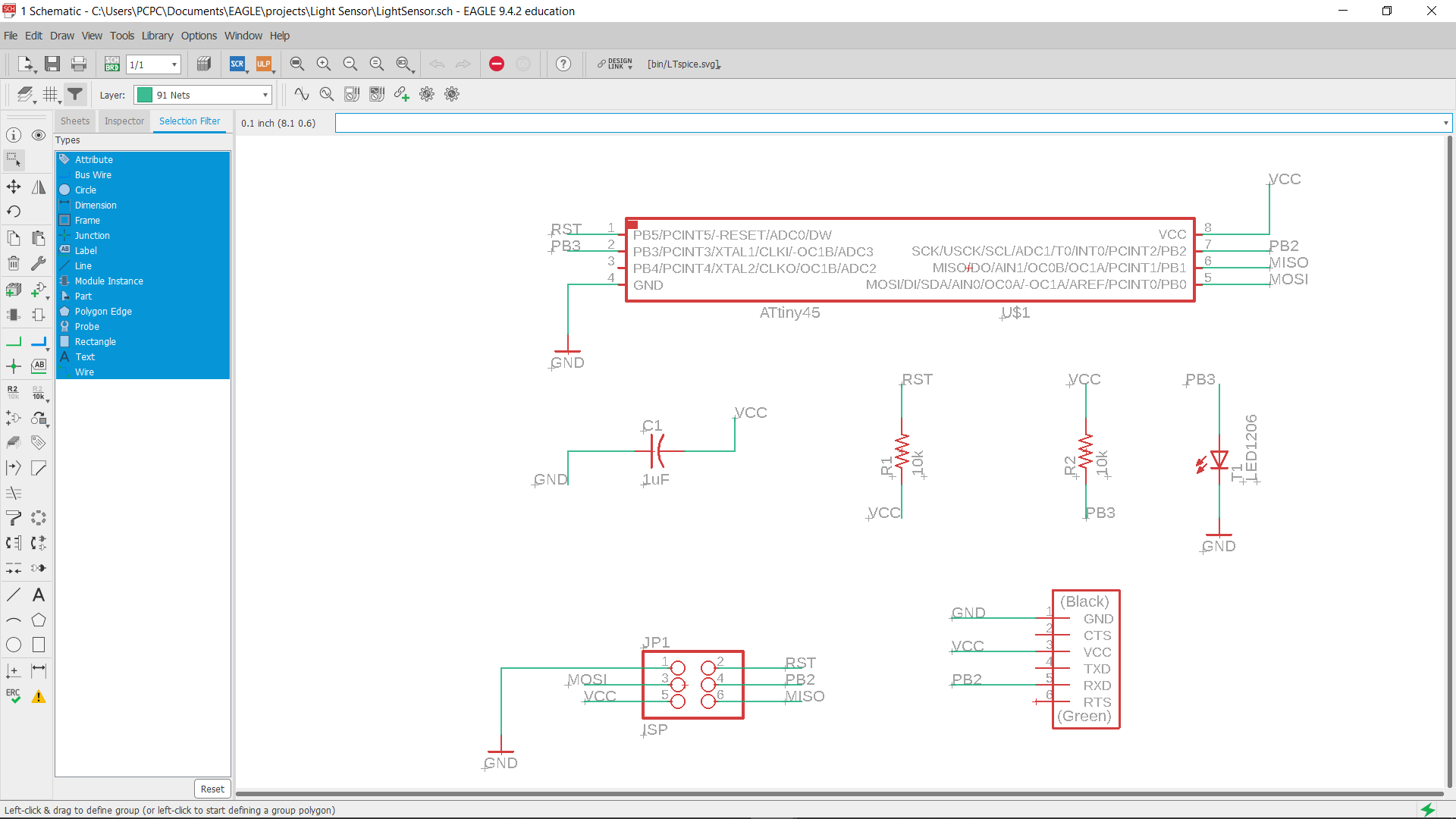
Board Design - Schematic
I started schematics in Eagle and after some time realized that there was a problem…the ATTiny44 pins (PA4 and PA6) utilized by the SDA and SCL pins of the GY-521…were also the same pins needed by the ISP header (to be connected to the FabTinyISP Programmer) for SCK and MOSI, respectively. No one in the lab was sure whether it was possible to either…
- Let the ISP and GY-521 connectors share the pins
- Or, set different pins for serial communication by the GY-521’s SDA and SCL Pins
Lots of discussion and investigation ensued…then it became late in the afternoon of the day’s work session, so I decided to abandon plans to use the GY-521…and make a simpler board that has the Accelerometer (ADXL343) only.
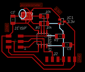
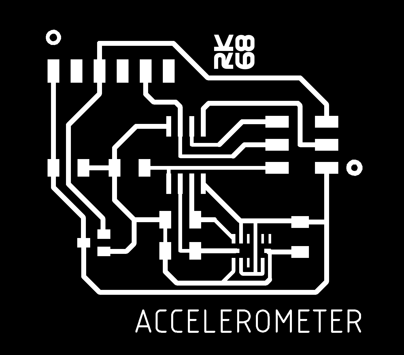
Referencing Neil’s board route diagram, I started new schematics for a Microcontroller and Accelerometer board that…
- Uses an ATTiny45 microcontroller (…not 44)
- Had a FTDI connector for power and serial communication with a PC
- Had an ISP connector to allow for programming via a FabTinyISP
- Had an ADXL343 Accelerometer sensor
- Had a regulator that would output a clean 3.3v needed by the Accelerometer
- Had 3 x 10k Resister
- Had 2 x 1uF Capacitor
Back to Eagle to draw up Schematics. Wanting to meet the spirit of the week’s assignment and design my own board, I decided to do better than just copy Niel’s board exactly (which would have made things easier…allowed me to get to the board programming and testing phase faster…but I didn’t take the easy path) and at least come up with a different layout for the components that he recommended (I frankly do not have any ability to know what components to include or not include…for lack of electronic understanding). However, the greater number of components made drawing and labelling more difficult somehow (late afternoon low blood sugar?).
The ADXL343 was not in the Fab Library in Eagle…I had to go to the Analog Devices website to get it here
- Registered on the Analog Devices website
- Searched for the ADXL343 in the Components page
- Downloaded Eagle EAD associated with the ADXL343
- Followed instructions to install the device as a new library (could I have just added the component to an existing library?)
Took forever to get the routing right…particularly confused with how to properly represent ‘Pull-up Resisters’ (more on this later…) out of the ATTiny45’s PB3 & PB4 pins to the Accelerometer’s SCL and SDA pins, respectively. (a BIG thank you to classmate Kae Nagano for her kind assistance). Turns out, this aspect of the schematic is fundamental/critical to I2C communication between the Microcontroller and the Accelerometer (more on this later…).
Learning Outcome - Schematics
- Instead of connecting every pin from one component to pins on another component…and creating a spaghetti mess of the schematic…I got comfortable with naming pins at the microcontroller and accelerometer chip…so that virtual connections can be made (ex: connect line end named of ‘PB3’ on the ATTiny45 with line end named ‘SCL’ on the ADXL343…without having to draw an actual green line between them). What is critical with this technique (I learned the hard way) is to make sure to use very specific name identifiers…not arbitrary or non-sensical names…as it will make airwires on the routing procedure easier and more correct.
The schematics seemingly complete (…later discovered that there were errors), I moved onto the routing challenge…
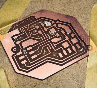
Board Design - Routing
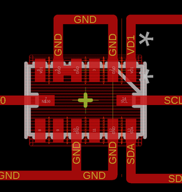
Finally…I got the board routed and PNG images generated for the board outline and trace (add files here). made routing mistakes…5v instead of 3.3v, cs not connected to VD1,
- Difficult to work with the small footprint of the ADXL343…even without routes, the pads of the stock footprint themselves were causing clearance issues between the pads themselves. Caterpillar sensei advised me that the footprint of the component can be modified. Cool!!
- Also added text to the board for the first time using Eagle’s text function…choosing ‘vector’ and changing text size…leaving all other settings as is.
Mistakes Made - Routing
- I made some critical mistakes here that I would only discover later
Neil’s board diagram…and where I made my mistakes…
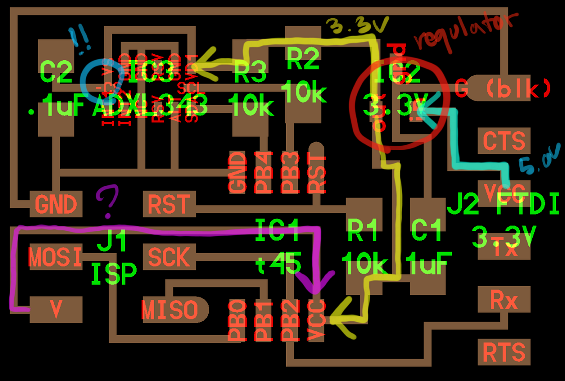
My initial routing and my mistakes indicated in light blue…
- I routed the power from VCC to the rest of the board incorrectly…allowing for 5.0v to reach components that should have received 3.3v (the ADXL343). In Neil’s diagram, VCC heads to the Regulator (blue line) where it is converted to 3.3v heading toe the ADXL343 and the ATTiny45 (yellow line). I probably fried the ADXL343 and maybe the ATTiny45 as a result.
- I didn’t bridge the VS pad to the CS pad under the ADXL343. This meant no power to CS…allowing it to be set to HIGH and allowing Serial communication
- I also chose to route the power line from the ISP header (purple line) to the FTDI header’s VCC…rather than from ISP header to ATTiny45 VCC. But I am a little confused as to why Neil would do this…as it seems it makes it possible for 5.0v to reach sensitive 3.3v components on the board. But my routing is probably problematic in some way too (…lack of electronics knowledge showing here)
Learning Outcome - Routing
- Not all power is the same…in the case of the Accelerometer board, ‘VCC’ cannot be arbitrarily used to power everything. I have to pay more attention to component power requirements and power routing in the future. In this case, The ADXL343 chip requires 3.3v power whereas ‘VCC’ is normally 5.0v. Neil’s board design contains a regulator (a MOSFET?) that steps down the voltage from 5v to 3.3v…the routing of power on his board design was very important and specific. This I did not appreciate and resulted in a lot of headaches for me during the ‘Board Design’ stage.
- The VS to CS bridging mistake involved a small detail that is critical to success…a mistake that would have been avoided with a proper understanding of the purpose of function of each pin. I was reproducing a ‘drawing’ whereas I should have been reproducing a functioning electronics ‘circuit’. Lots of learning ahead…but a good lesson on a required mindset shift.
Work Session: Day 2
Board Fabrication
Using MODS…generated RML files from the PNG images generated by Eagle.
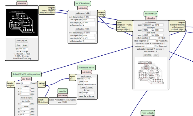
Procedure: Add Roland SRM20 Module programs open server programs roland srm20 > PNG PCB
Procedure: Add Save to File Module (Kamakura’s machine not connected to network) modules open server module file > save (connect to Roland srm20 milling machine module via Outputs > file…i.e. left click ‘file’ in both modules to draw a connecting line)
Procedure: in roland srm20 module.. - change origin to 0,0,0 - choose 1/64 for trace…1/32 for outline - click calculate in ‘mill raster 2d module’ - click ‘view’ to examine the mill path of the trace…noted a few places where the space between pads were not milled…since I already modified the pad in Eagle already…will try another technique to fix: indicate the mill bit diameter as smaller (?) than actual (why?)
Milling goes smoothly (whew!!! Something went right!)
Stuffing
ADXL343…what little feet you have!!!
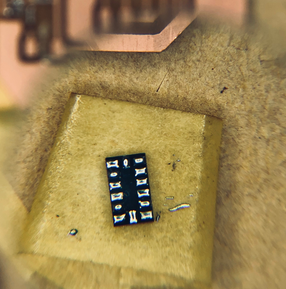
Soldering the very small ADXL343 with its pads underneath the chip is REALLY difficult. I couldn’t find a way to get comfortable with trying the ‘Reflow’ technique (running behind schedule and not wanting to fail…) mostly because I just didn’t know how to hold the heat gun keep the ADXL343 in position at the same time. Decided to stick to soldering techniques that I know (one of my classmates successfully soldered an ADXL343 in place doing this).
Figured I would work on the hard component first and solder the AXDL343…a procedure that ended up burning 1.5hrs of my time (yeah, pathetic!).
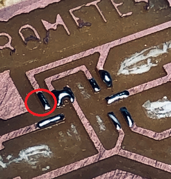
- Pre-tinned the tiny pads on the board
- there is a mistake here circled in RED, which will contribute to the board not working later…
- Note that I scraped away some of the ‘Inactive’ pads…wanted to reduced the possibility of accidental bridging…not sure if this was a good idea.
- Pre-tinned the tiny pads under the ADXL343
- I kept it still using some tape
- Not certain that I needed to tin the ‘Inactive’ pads too…especially since I removed the corresponding pads on the board
After several flawed and failed attempts and tons of time used (…I have destroyed 2 ADXL343 chips so far), I managed to get the ADXL343 soldered onto the board (…with the critical mistake of the CS and VS pads properly bridged). The rest of the ‘stuffing’ work went more quickly (…but full of flaws).
Learning Outcome - Stuffing
I have some ideas for getting Soldering of tiny components like the ADXL343 right…
- Make certain not to leave rounded blobs of solder on the board pads…a flatter platform for the ADXL343 to sit on in preparation for reflow soldering means greater ease in keeping it in the right position (instead of sliding this way and that on top of rounded solder pads)…wick away some of the solder to leave tinned but flat pads
- Use a (clean, new) sharper point tip on the soldering iron…to make contact between the iron and the ADXL343 pads as exact as possible when pre-tinning the board and ADXL343 pads.
- Fix the ADXL343 upside down on a fixed surface to make pad pre-tinning a little easier and more precise. Can drag tinning be used?
- Flux the pads on the board and chip prior to tinning…to make for cleaner tinning (?)
- Possible technique to reflow…can legs be soldered to the bottom to the ADXL343, pointing out to the side (like the legs of a bug)…to make soldering on the board easier?
Board Programming & Testing
Programming the board using the FabTinyISP. Enter the following 2 commands in succession in GitBash (NOT Windows Command Terminal!!!).
make -f hello.ADXL343.make
make -f hello.ADXL343.make program-usbtiny
Note: The typical second ‘make -f hello.ADXL343.make program-usbtiny-fuses’ command not used here…because no external crystal/clock/resonator used on the board*
Failure to launch…the Frankenstein
When a serial connection was made in Arduino IDE, the resulting data output was non-sensical gibberish (a continuous string of random ASCII characters)…not values for X, Y and Z as would have been expected. 3 other boards were made after this first attempt (that corrected the routing mistakes of the first)…but all of them produce gibberish as output. Without any more time to spend on fabricating this board, I have concluded the following…
- Hand soldering this little component with many pads underneath is beyond my current capability.
- I tried to reflow rather than solder…but could not get the sensor to stay in place while I tried to manipulate the heat gun (we don’t have one in the lab with a small nozzel) and a tool to hold the chip down (like the pliers used in Neil’s reference picture)
- The use of the soldering iron, particularly because I probably had it in contact with the sensor for too long…was probably that I destroyed the sensors (the datasheet warns that high temperature tolerance is only a few seconds)
- Time permitting…I should test the board using an oscilloscope to see what kind of signal wave the sensor is outputting.
- Reflow is certainly the answer…but perhaps with a solder that melts at a lower temperature like Bismuth (rather than the traditional Tin/Lead solder).
Work Session - Day 3
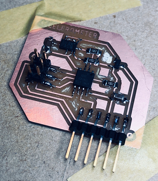
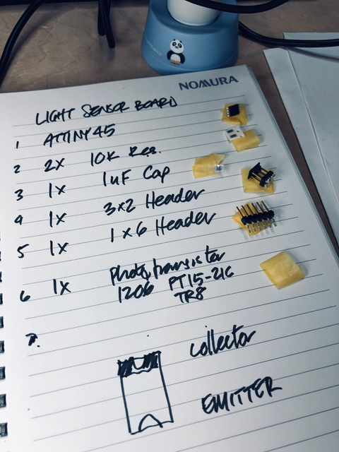
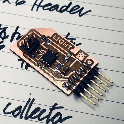
Several weeks after the failed attempts to get an Accelerometer board to work, I produced a PhotoTransistor, Light Sensor board in preparation for my Final Project.
Completing the Assignment - Phototransistor Board
For my final project, an ambient light sensor is a critical component. So I made a Phototransistor board based on Neil’s example. Thankfully this board proved a success.
Research
Data Sheet Learnings - PT15-21C/TR8 Phototransistor
The datasheet for the PhotoTransistor can be viewed here
- This complicatedly named, SMD PhotoTransistor, manufactured by Everlight
- Capable of measuring both visible and infrared ambient Light
- Requires 5V and 20mA of current only, to operate
- It is a rather simple device that bears similarity with and LED in form factor and also required polarity orientation…the ‘Collector’ end connected to power and signal pin while the ‘Emitter’ end connected to GND.
- The datasheet, 8 pages long only, indicates that the ‘Collector’ end of the PhotoTransistor is indicated with a green mark. I used this to make sure it was soldered on in the correct orientation.
- The sensor is VERY sensitive to heat and the datasheet recommends limited contact time with the soldering iron heat (3secs max)
ADC - Analog-to-Digital Converter and the Phototransistor
(Research on PhotoTransistor conducted here)
PhotoTransistors convert incident light to electric current, when photons activate the transistor. A 3 terminal device consisting of Base, Collector and Emitter leads. In a CE configuration, light causes the output to go from HIGH state to LOW state. In CC configuration, it is the opposite. Can be used in ‘Active’ mode (an Analog element with linear output proportional to light intensity) or ‘Switch’ mode (a digital element in either a ‘cutoff’ OFF state or ‘saturated’ ON state).
The ADC takes analog signal generated by the PhotoTransistor and converts them to a digital signal…”converts a continuous-time and continuous-amplitude analog signal to a discrete-time and discrete-amplitude digital signal”. (wikipedia) The bandwidth of the an ADC is characterized primarily by its ‘Sampling Rate’.
ADC on the ATTiny45 - The Analog-to-Digital Converter (ADC) is discussed in section 17 (…from page 121-137) of the datasheet - According to the datasheet…the ADC converts analog input voltage to a 10-bit accurate digital value, with the minimum value represented by GND and the maximum value represented by the ‘Reference Voltage’ (which can be the VCC supply, AREF pin or Internal 1.1V reference) which indicates the conversion range for the ADC. - 10-bits means that analog inputs will be represented digitally by integers from 0 to 1023 - The ADC is optimized for analog signals with an output impedance of approximately 10k Ohm or less. The PhotoTransistor impedance is not specified in its datasheet however. - On the ATTiny45, 4 Analog pins (1,2,3,7), are capable of ADC functions on external input signal sources.
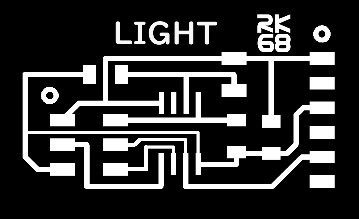
Schematic design
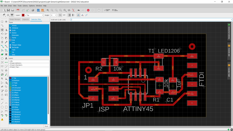

Milling & stuffing
A very simple board. Milling and stuffing went smoothly.
Programming
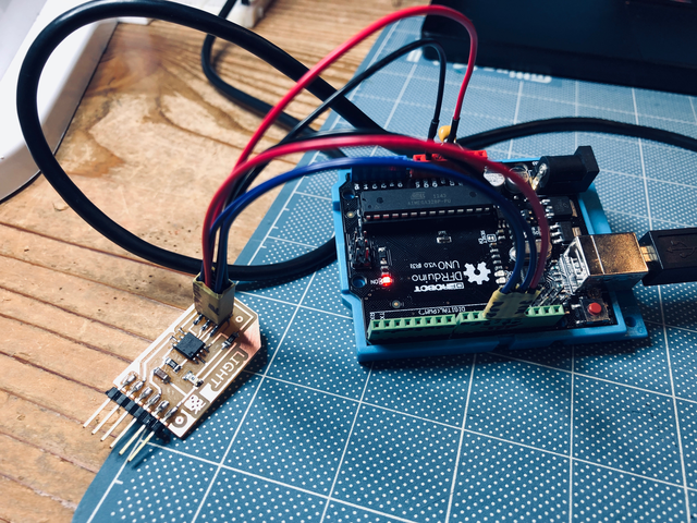
Rather than use make files to upload Neil’s code, I programmed the board with an Arduino sketch (using, for my first time, the Arduino as the programmer) which I intend to utilize in part in my final program.
The procedure to use the Arduino as an ISP programmer as follows… 1. Prepare the Arduino as an ISP programmer - Prepare the target board to receive Arduino code with a ‘bootloader’ program - Upload an Arduino program to the target board
Testing
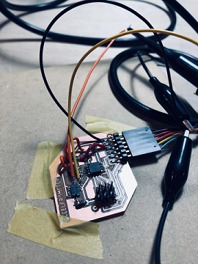
After uploading the program to the Phototransistor board (connected to my PC via an FTDI cable) and connecting to Arduino’s Serial Monitor (after switching to COM4 and setting the Baud Rate to 9600)…the board could successfully read and display light levels.
See video with Processing interface graphical output (written by classmate Kae Nagano) here
Another video showing serial data output via the Arduino IDE serial interface here
My simple code used to run the test on the Light Sensor (PhotoTransistor) here (SoftwareSerial library required to run on Attiny chipset)…
// Phanuwit Kanthatham, FabAcademy 2019, FabLab Kamakura


#include <SoftwareSerial.h>

const int LuxPin = A3;  // Sets constant variable for Arduino pin A3
                        // ...as the analog signal pin to Lux sensor

SoftwareSerial LuxSerial(1,2);

void setup() {
  LuxSerial.begin(9600);       // Starts up serial communication
  pinMode(LuxPin,INPUT);       // Sets the A3 pin where the Lux sensor
                               // ...is connected as INPUT

}

void loop() {
  int LuxVal = analogRead(LuxPin); // Reads analog values from PhotoTransistor sensor

  LuxSerial.print(LuxVal);        // Prints PhotoTransistor value in serial monitor
  LuxSerial.print('\n');
  delay(500);           // Wait 500ms before reading from the sensor and printing value again

}
Files
Accelerometer schematic file here
Accelerometer routing file here
Accelerometer trace image file here
Accelerometer outline mill path file here
Accelerometer trace mill path file here
LightBoard schematic file here
LightBoard routing file here
LightBoard outline image file here
LightBoard trace image file here
LightBoard outline mill path file here
LightBoard trace mill path file here
Appendix: Additional Research
The Challenge with accelerometer
Before even entering the lab to do work, a lot of discussion ensued with regards to the tiny, SMD Accelerometers and the ‘Reflow’ solder techniques that would be required to mount them to a board…because the device has a ton of pads…and they are all underneath the device itself. The soldering techniques we have been using so far will not work.
Enter the solder paste… - Bismuth/Tin…lead free - Other Lead-Free solder has a high melting temperature (280 deg)…Tin/Silver/Copper (SAC)…good but more brittle
The Wonderful World of Solder…
I learned much about ‘Solder’ of this from this video, by iPad Rehab…skip the first 5:30mins though…
Leaded Solder - Sn63Pb47 - …which is code for 63% Tin, 47% Lead…is considered ‘the best’ solder because it is robust, strong, malleable and makes great joints…Eutectic, melts at specific temp of 183 degrees - 63/47 is used by the military grade electronics, the space shuttle - Lead is a Neurotoxin…it is bad bad bad for you.
Bismuth Solder - Sn42/Bi58. - ..Tin/Bismuth…melting temp 138 degrees - another SN/Bi…melts at 172 degrees - …if SN/Bi is mixed to form an alloy with Pb…then the melting temp drops to dangerously low 42 degrees…need a separate soldering iron that isn’t ever used to work tin
Silver/Copper/Tin Solder - SnAgCu - The most common ‘Lead Free’ solder used in electronic manufacturing…used in iPhones - Melting temperature:
Modifying A Component’s footprint**
- In Eagle, go to Library Manager
- Select the component to be modified…the ADXL343 in this cause
- Select ‘Edit’…double click on the pad needing adjustment and change its size in properties (Tip: make sure to take note of the initial size of the thing to be modified before going crazy with changes). I choose to make 10 of 14 ‘Active’ pads slightly more narrow and making the 4 of 14 ‘Inactive’ pads very narrow.
The ADXL343 Accelerometer Datasheet - Expanded Notes
- A MEMS by Analog Device
- Replaces the ADXL345…code for 345 will work with 343
- Polysilicon surface-micromachined structure built on top of a silicon wafer…deflection of the structure is measured using differential capacitors.
- Triple-axis accelerometer with digital I2C and SPI Interface pins
- Measures both dynamic acceleration resulting from motion or shock and static acceleration, such as gravity, that allows the device to be used as a tilt sensor
- Wide sensitivity range and high resolution…
- sensitivity can be set to +/-2g (for slower movements), +/-4g, +/-8g, or +/-16g (for high speed tracking)
- measurement range is selectable
- 10 or 13-bit internal ADC (Analog-Digital Converter) Built in motion detection…makes tap, double tap, activity, inactivity and free-fall detection easy…these functions can be mapped individually to either of the 2 interrupt pins
- Integrated memory mgmt system with 32-level first in first out (FIFO) buffer to store data and minimize host processor activity and lower power consumption
- Libraries for Arduino(C/C++) and CircuitPython (Python 3) available
ADXL343 Pins:
Power Management
- Vs (Pin 6): Supply Voltage
- VDD I/O (Pin 1): Digital Interface Supply Voltage
- power can be supplied to Vs or VDD I/O in any sequence without damaging the ADXL343
- …interface voltage level is set with the interface supply voltage VDD I/O, must be present to ensure no conflict on the communication bus
- …Vs must be greater or equal to VDD I/O in Dual-Supply application, to accommodate the desired interface voltage
- …when Vs is supplied, the device enters Standby mode, waiting for VDD I/O to be applied and command to enter measurement mode to be received (setting the ‘Measure Bit D3’ in the POWER_CTRL register (Address 0x2D)) -…in Stand-by mode, any register can be written to or read from to configure the part
- …Recommended to configure the device in Standby mode and then enable measurement mode
- …clearing the measure bit returns the device to standby mode
- …to prevent communication bus conflict, have the Bus Enabled (Vs = OFF, VDD I/O = ON)
- …to enter Low Power Mode, set LOW_POWER Bit 4 in the BW_Rate register (Address 0x2C)…some data rates benefits from low power Mode
Control & Interrupt Logic - CS (Pin 7): Chip Select - …I2C is enabled if the CS pin is tied HIGH to VDD I/O, there is no default mode if the CS pin is left unconnected (so should always be tied HIGH to VDD I/O, communication with ADXL343 not possible otherwise) - …in SPI mode, the CS pin is controlled by the Bus Master - INT 1: Interrupt 1 Output - INT 2: Interrupt 2 Output
Serial I/O - SDA/SDI/SDIO (Pin 13): Serial Data (I2C)/Serial Data Input (SPI 4-Wire)/Serial Data Input and Output (SPI 3-Wire) - SDO/ALT Address (Pin 12): Serial Data Output (SPI 4-Wire)/Alternalte I2C Address Select (I2C) - SCL/SCLK (Pin 14): Serial Communication Clock …SCL(I2C)/SCLK(SPI) - …I2C and SPI digital communication are available, in both cases the ADXL343 operates a ‘Slave’ - …In both SPI and I2C modes, data transmitted from the ADXL343 to the master device should be ignored during writes to the ADXL343 (??)
Other - Reserve (Pin 3 & 11): Connected to Vs or left open - GND (Pin 2, 4 & 5): must connect to ground - NC (Pin 10): Not internally connected
I2C
- Also known as 2-wire Interface
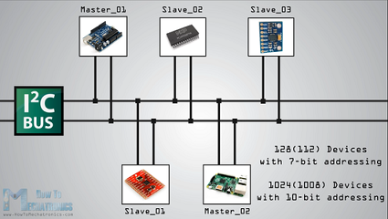
- What is I2C? The Inter-integrated Circuit (I2C) Protocol is a protocol intended to allow multiple “slave” digital integrated circuits (“chips”) to communicate with one or more “master” chips, I2C connection requires only 2 wires (SDA and SCL) it is very useful in low pin microcontrollers.
- Tell slave devices what to do or receive data from them...
12C explained
A couple of videos here and here
- easily implemented, when communication between master and multiple slave devices…or even multiple-masters…needed
- only 2 wire are required for communication…up to 128 devices with 7-bit addressing, 1024 devices when using 10-bit addressing
- Serial Clock (SCL)…clock signal generated by the Master device, synchonizes the data transfer between devices on the I2C bus
- Serial Data (SDA)…carries data
- …the two lines are ‘open drain/collector’ configuration…’pull up resisters’ need to be attached to them so that the lines are High…the devices attached to the line are active Low…create two stable voltage states
- resisters commonly used, 2k for higher speed up to 400kbits/sec to 10k for /100kilobits/sec
- made possible…each device has a preset ID or unique device address…the master can choose which device to communicate with
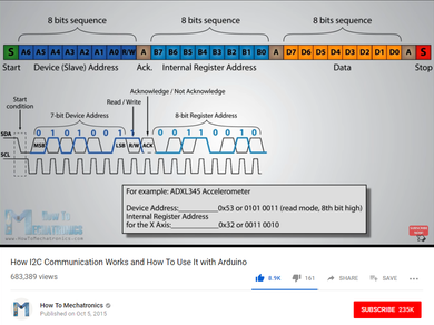
- The Data flow…I2C
- 1 bit start condition…when SDA drops LOW, while SCL still HIGH
- 8 bits “Slave Device address”…to which the data is being sent…7 bits…the last bit is HIGH or LOW indicating READ or WRITE
- 1 bit ‘acknowledge’ (pull SDA line DOWN)…if not acknowlege (SDA line UP)…used by Slave device to indicate receipt error…slave busy, lack of understanding of instructions, cannot receive any more data…if unacknowledged, Master decices how to proceed
- 8 bits…”internal register of the slave device”, locations in Slave memory…ex: the X-Axis register
- 1 bit ‘acknowledge’
- 8 bits ‘data sequence’…repeats until all data sent…either by Master or Slave depending on condition at previous READ/WRITE bit (8th bit of 1st sequence)
- 1 bit acknowledge
- 1 bit stop…when SDA goes from LOW to HIGH…while the SDL line is HIGH
- A good idea to print out the datasheets of the Slave Devices…to know what signals to send to do what specific action
Note: Breakout Boards already have pull-up resistors. Note: There are other communication protocols…SPI, One Wire Interface, etc.
I2C on ATTiny44
Good tutorial on Instructables here
- ATTiny44 has USI (Universal Serial Interface) making I2C communication possible…as slave or master
- a 1MHz AVR can manage a standard 100kHz I2C bus
- a 8MHz AVR can manage a 400kHz I2C bus
- communication speed is selected in the USI control register
- Master always controls clock speed
- Microchip MCP23017 GPIO Expander…16 bits of additonal GPIO over the i2c bus
- Oscilloscope with 2-channel…i2c has 2 wires
- “Open Drain” = outputs of all connected devices cannot directly output a logic-level 1 (HIGH)…only logic-level 0 (LOW)
- “Pull-Up Resistor” = make the line go HIGH…all devices release their pull on the line (one each for SDA and SCL) and a Pull-Up Resistor between the line and the positive rail pulls the voltage up…1-10k Ohms good…low enough that the signal can be seen as a high level by all devices but high enough can be easily pulled down (shorted out) and not cause damage
- i2c is a ‘synchronous’ serial data transfer…made possible by clock signal from the master and present to all connected devices (RS-232 is example of ‘asyncronous’…pre-determined time-base or baud rate)
- Serial = one single bit transferred at a time over a single wire…vs Parallel data transfer…multiple wires each carrying one bit, sampled at once, multiple bits in Parallel
- Bus = a system allows many devices to communicate over a single wire; i2c is a bus…allows a new device to connect by attaching their SDA and SCL connections to an existing line. Busses uses an addressing system, each device has a unique address…simple binary number
wiring example here
I2CdevLib page here