This week, we built an In-System Programmer (ISP), which is a tool to program other microcontrollers that are already built into their circuits. As the board we will build contains a microcontroller, we need to have a working ISP ready to program it, so it can become an ISP itself. I did this assignment parallel to the electronics production assignment, because they are quite similar and conceptually close. Even with basic prior knowledge in electric circuits, this was no easy task. Fortunately, I did not need to reinvent the wheel: I oriented myself on an ISP design by Brian, and on the documentation of Matthias, a student of our lab from last year.
What's on the board
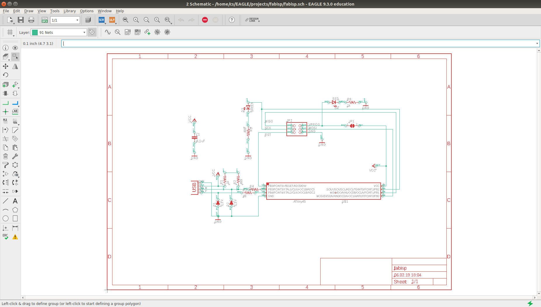
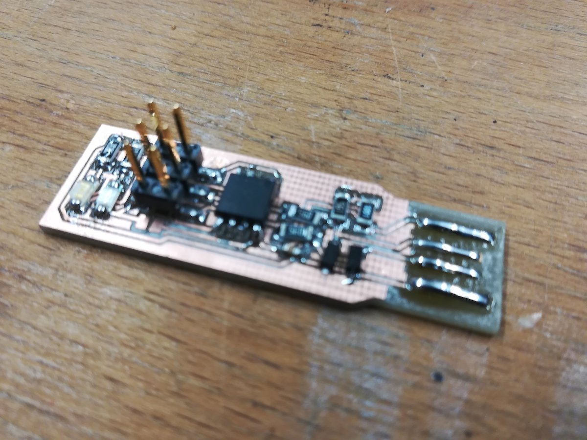
The board's main part is an ATTiny45, which is connected to a USB connector. There is also a six-pin header which connects to the target board, and two LEDs; a red one that indicates when the ISP delivers power to the target board, and a green one that lights up when the ISP is talking to the target board. The two zener diodes act as a voltage clipper, ensuring a maximal voltage of 3.3V on the data lines.
Unfortunately, I had not quite the same material available that brian used for his board.
I used slightly larger resistors (560Ω and 56Ω instead of 499Ω and 49Ω) and zener diodes with a zener voltage of 3.6V.
This does (for whatever reason) not work.
My PC would not detect the ISP with these resistors (see below).
Once I changed them for smaller ones -- 470Ω and 47Ω, respectively -- the ISP was recognized.
To make this ISP, we need the following:
Tools:
- A PCB mill (our lab has a LPKF Protomat)
- A soldering iron
- Soldering tin or (preferably) soldering paste
- An ISP to program the ATTiny
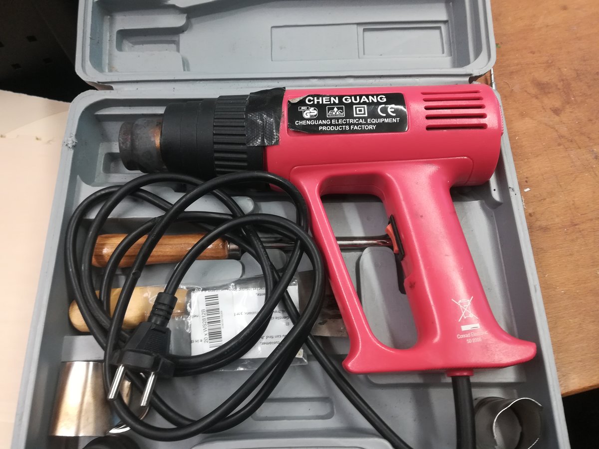
- If you're using soldering paste, I recommend using a reflow oven or a hot air gun instead of a regular soldering iron.
Parts:
- single sided PCB material
- ATTiny 45
- resistors:
- 2x 1kΩ
2x1x 560Ω2x 56Ω2x 47Ω- 1x 470 Ω
- red LED
- green LED
- 2x zener diodes 3.6V
- 100nF capacitor
- 2x3 pin header
- 1x2 pin header as jumper (optional)
To recreate the schematics and board files (or to adjust them), we also need a software to create and/or work with them; see the next part for an example, or skip ahead to see how to mill and program the ISP.
Creating the schematics and board layout
I used Eagle from Autodesk to sketch the schematics and the board. There is a free (but limited, mostly in the maximum board size) version available. Eagle is professional software; it probably can do whatever you want it to do, but you probably have no clue how. Fortunately, there are nice tutorials and setup guides available. I followed the one from Sparkfun (setup, schematics, and layout), because I also used their library of parts. Additionally, I used the fab library and the usb connector is from a nice collection of libraries on github.
Working with Eagle
First, we have to create the schematics of our board, that is, an abstract visualization of what parts there are on the board and how they are connected. Then, we do the actual board layout. This involves placing the parts, routing their connections, and making sure everything fits in the available space. Finally, we use the CAM processor to export files for the PCB milling machine.
Drawing the schematic
First, we draw the schematics of our board. In Eagle, every tool has to be selected in the left menu, and then applied somewhere in the main window. It's also possible to type in a command in the bar at the top and then to select where to apply that command.
First, we add the parts that we need for our board with the "Add Part" tool. For a lot of parts that can be bought there is some Eagle library available; you just have to find the right one. I used the following libraries:
- The Eagle standard libraries
- The libraries provided by Sparkfun (also available in Eagles library manager)
- The fab library
- This library for USB ports I found on github.
So we just go ahead and add all required parts to the schematic, using the "Add Part" tool. For the resistors, I used a generic resistor symbol. To give your schematic a tied-up feeling (and make it look more professional), you can add a frame (just search for "frame" in the available parts). Don't forget to add at least one VCC and one ground. Next, we want to connect those parts with nets; choose the "net" tool on the left (do not confuse it with the "wire" tool). When everything is connected, arrange it in a way that seems the most clear to you. Then click on "File"->"Switch to Board" to open the view that lets you do the routing of your board.
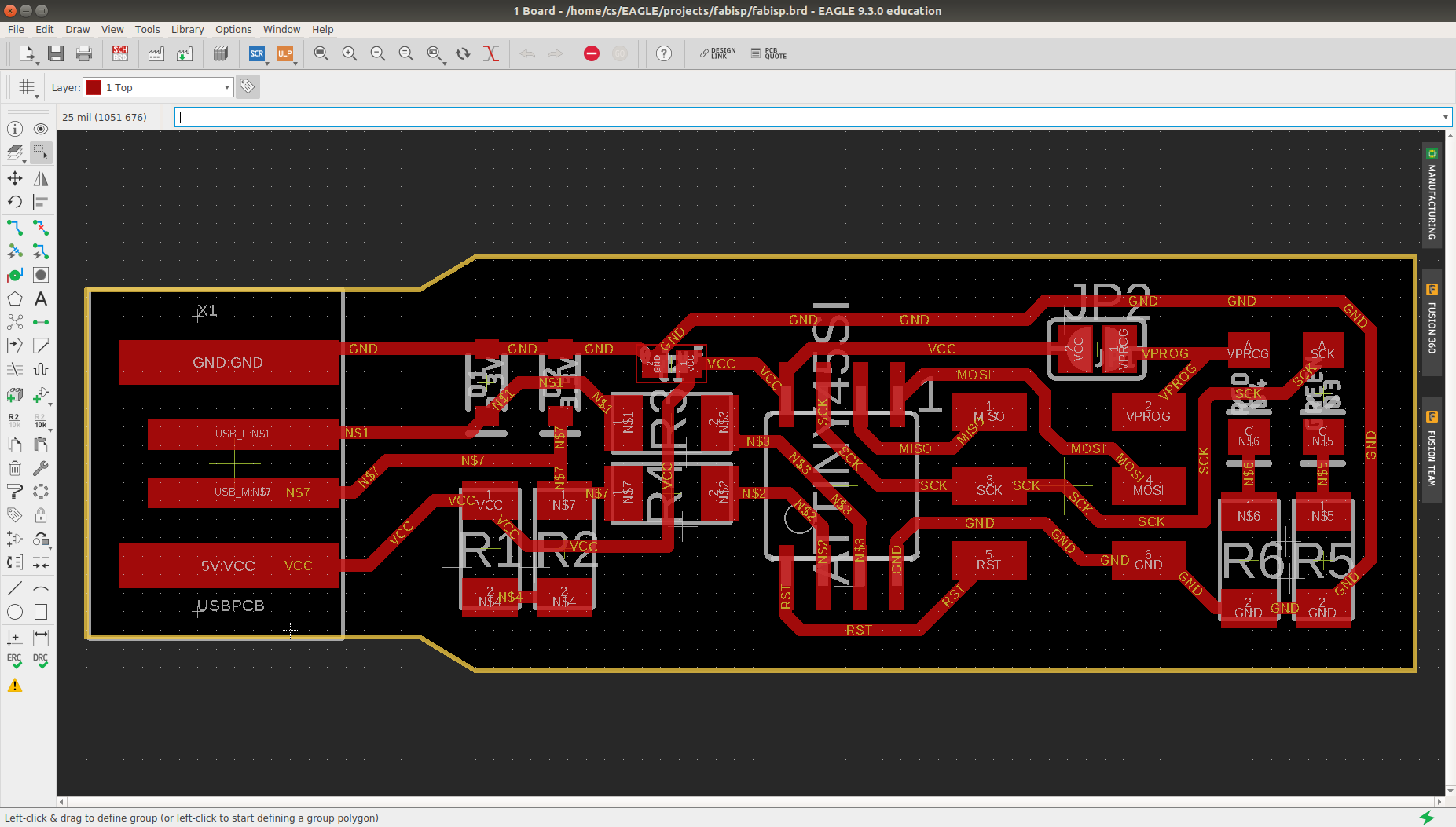
Board layout
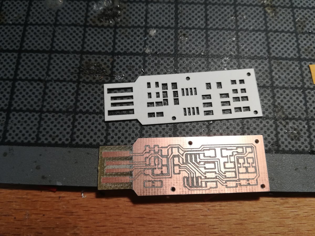
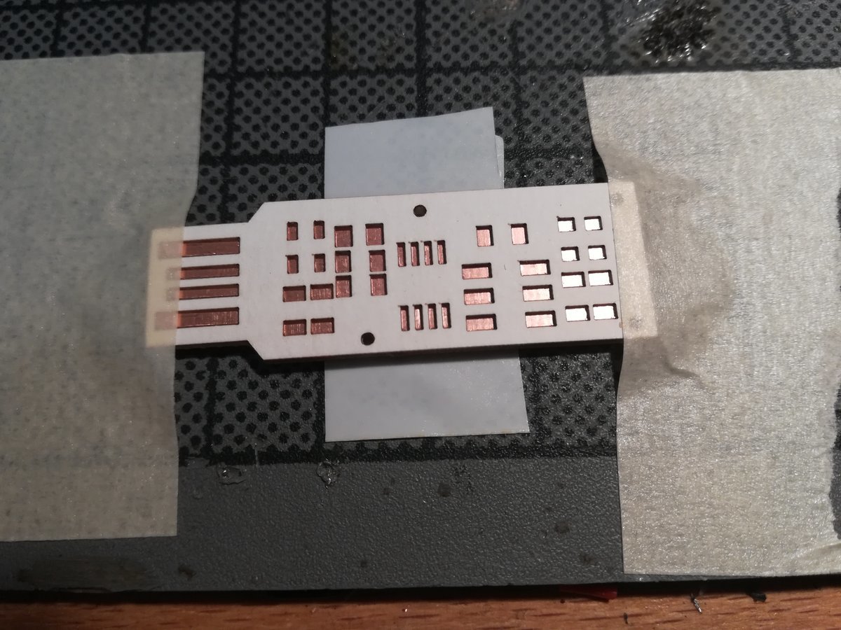
After completing the schematics, it is time to layout the actual board. Ideally, we want to place everything as neatly and as near together as possible to save space -- and therefore money and time that is needed to mill the board. A couple of things are important when creating the board layout: the 100nF capacitor has to be placed close to the ATTiny and VCC, otherwise it is not useful. And the other thing to have in mind is the width of the copper traces, which have to be at least thick enough to be milled by your PCB mill. I choose a width of 16 mil, which is more than twice as thick as the thinnest route the mill is capable to make reliably (which we tested during our group assignment).
Exporting CAM files
Before we can mill the board, we have to export a set of files. We use the "CAM Processor" of Eagle for this task. It produces gerber files, drill files, drawings, etc. based on a job description. We could probably just use the default single-layer job coming with Eagle, but there is an example job available on our lab page. Unfortunately, it uses some kind of legacy format; Eagle can automatically convert it to the new format, but there is a compatible version of EAGLE available on the PC connected to the mill. This job generates the following files:
- *.BRD: board outline
- *.TOP: top layer
- *.BOT: bottom layer (actually not necessary for this simple single-sided board)
- *.DRD: drill file (is not generated for boards without holes/vias) Now we can go and try to mill the board!
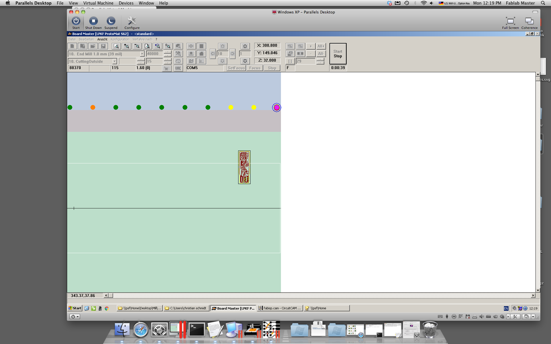
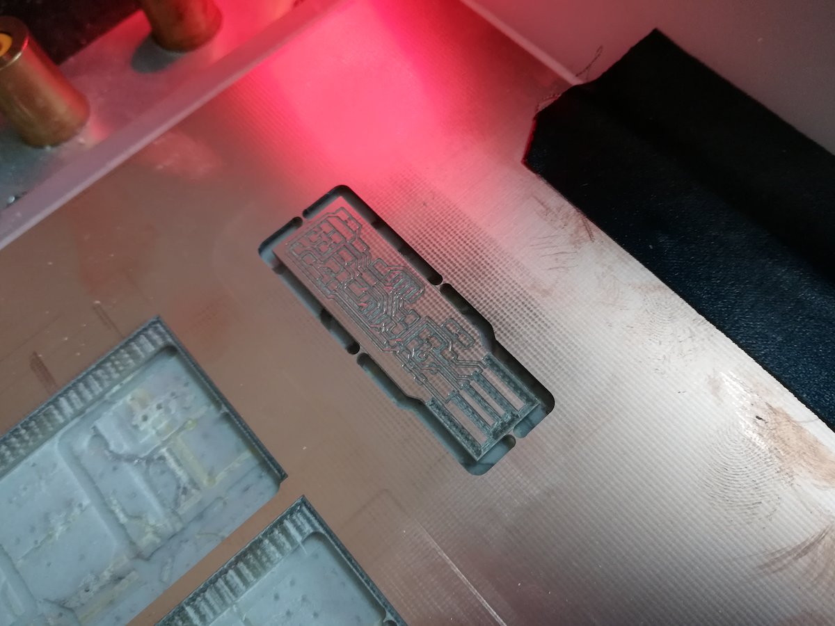
Milling the board
For the milling machine in our lab, there is an extensive tutorial available on our lab page, so I will only list the most important steps here.
On the machine controlling the mill, we start two programs: CircuitCam, to preprocess our board shape, and Board Master, the driver software of our mill. There will pop up several warnings and possibly some error messages, which are documented in our labs tutorial and which are not relevant here.
First, we open the files generated in the last step in CircuitCam. Here, we define the outline of our board, add bridges so that the board is hold in place while milling, add rub outs, i.e. portions of the board where unnecessary copper should be removed.
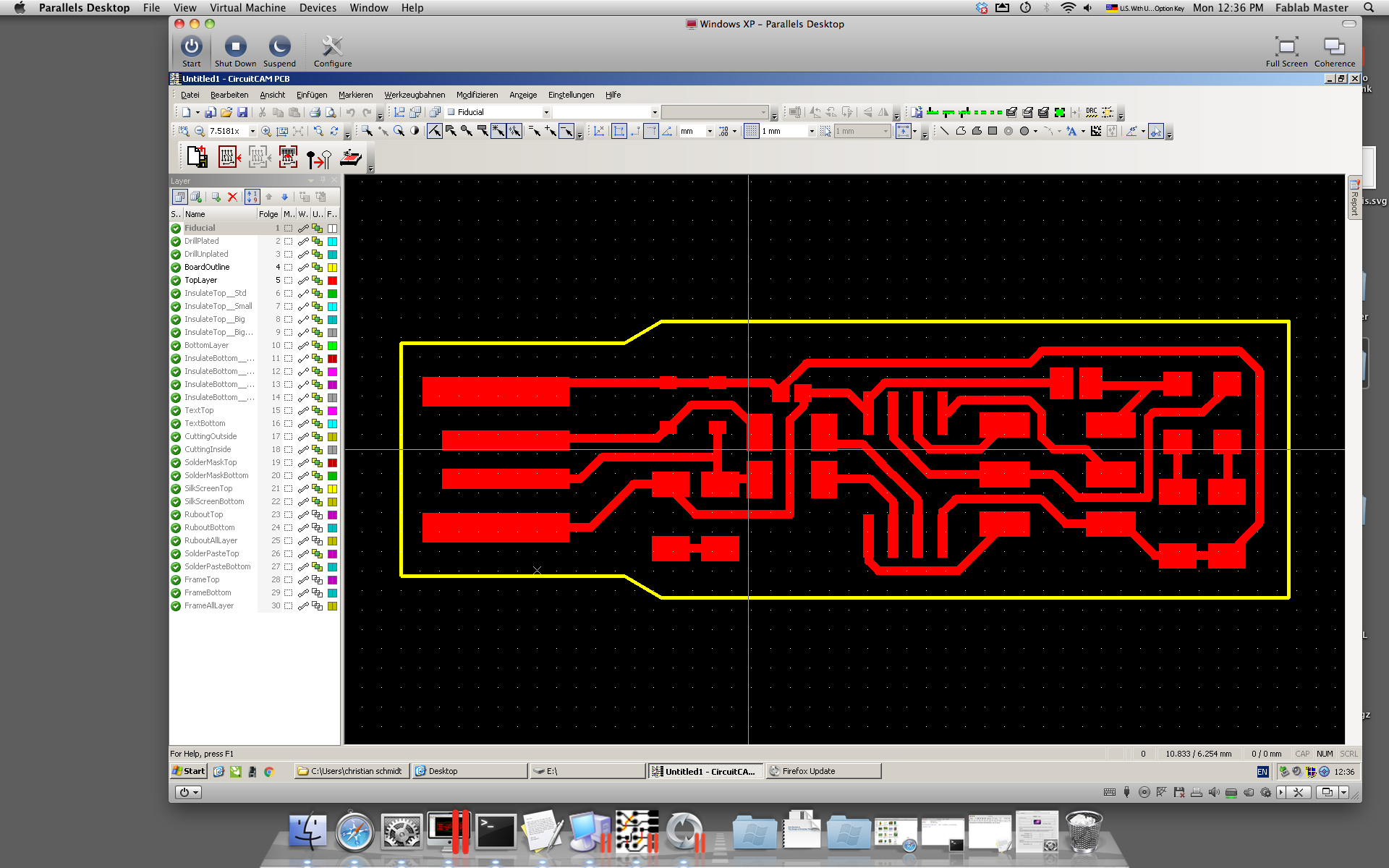
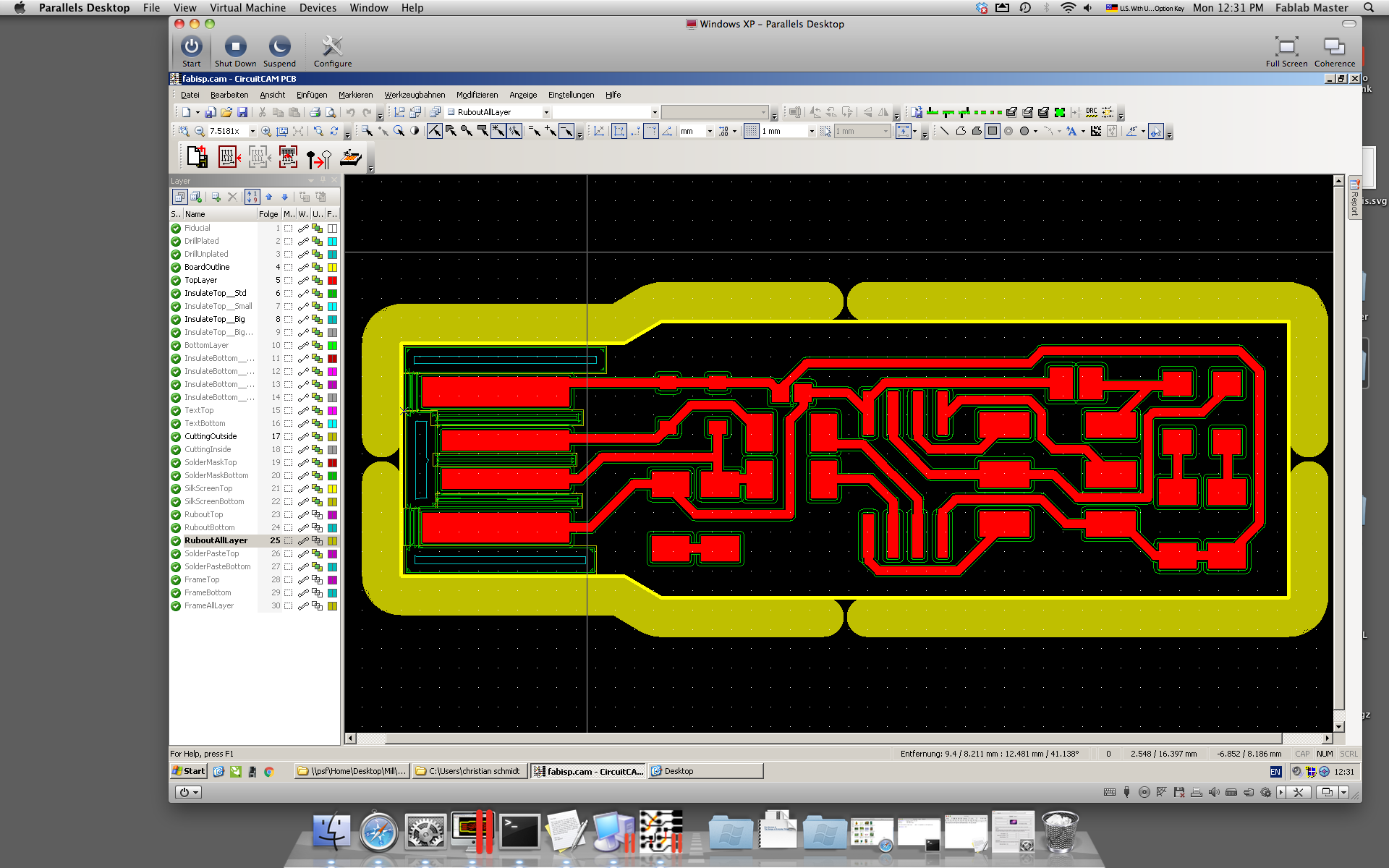
When we export the preprocessed board in CircuitCam, it is automatically passed on to Board Master, where we can move the board and the drill head to a suitable position. The milling process is divided into a number of steps, which have to be manually activated and started in Board Master. For this board, we only have to run "MillingTop" and "CuttingOutside" (for a more complete breakout of steps, check the tutorial.
The mill in our lab is a professional PCB mill which automatically chooses the right feeds, speeds, and even the correct tools to mill the PCB. The machine is able to switch tools automatically, so there is little to no manual intervention during the whole milling process. Most often, the machine is equipped with the following drill bits: 0.2mm fine cutter, 0.6mm, 0.7mm, 0.8mm, 0.9mm, 1.0mm spiral drills, 1.0mm and 2.0mm contour router, and a 1.0mm end mill. The traces are usually milled with the 0.2mm fine cutter.
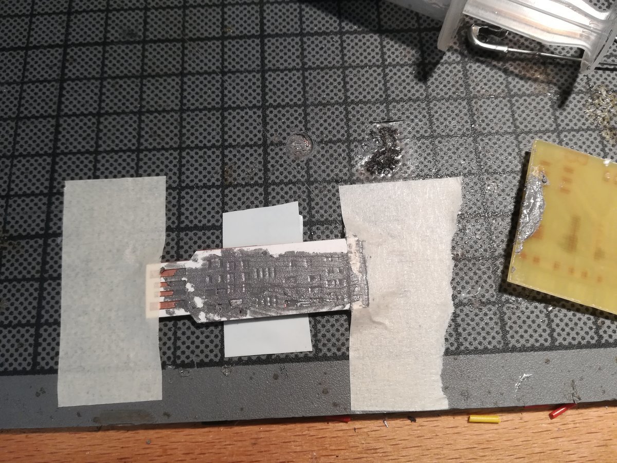
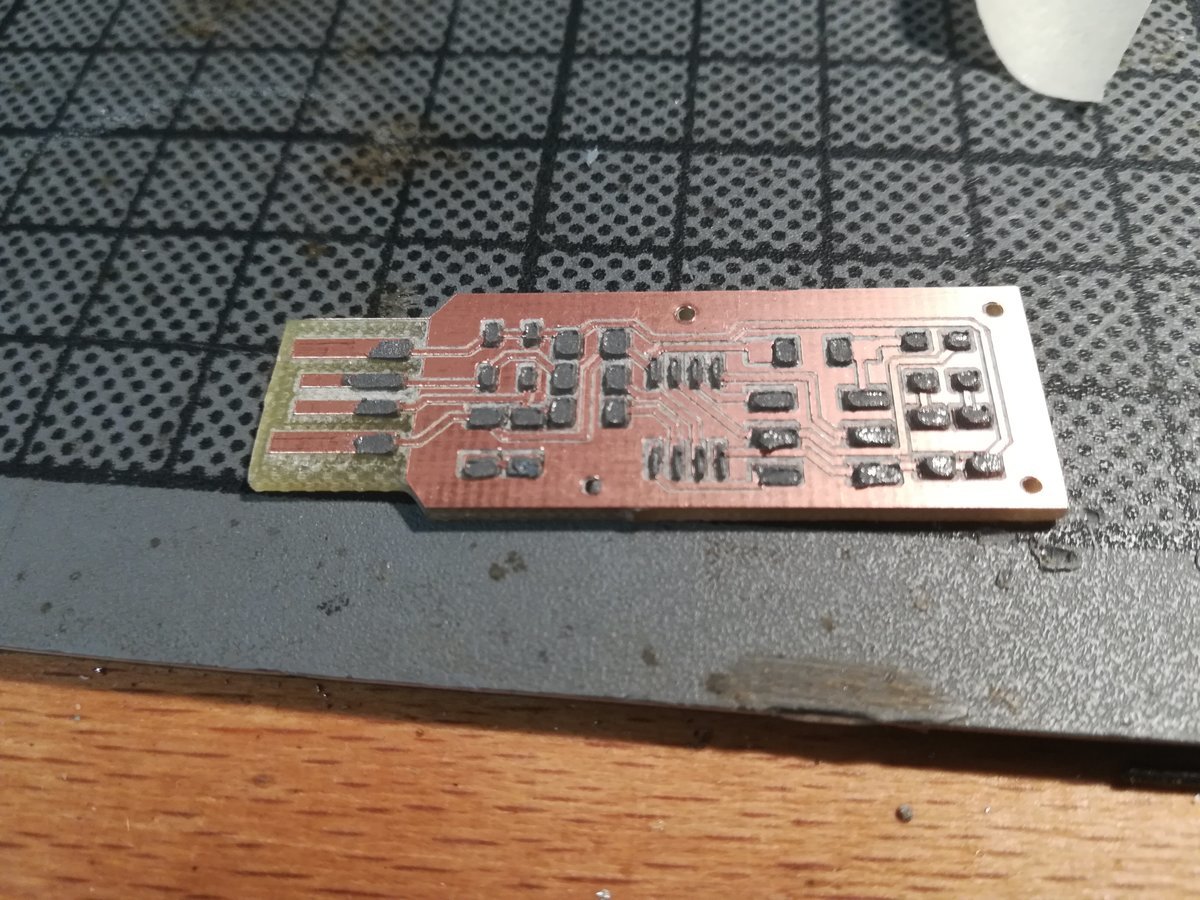
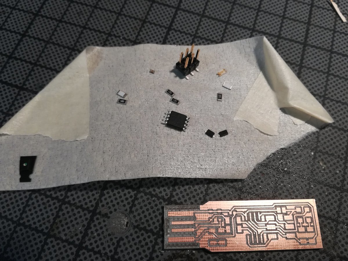
Soldering the components
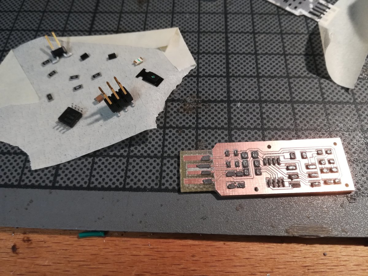
Now it's time to "stuff" our board, i.e. add the microcontroller, resistors, LEDs and all the fun stuff.
First off, I made some suboptimal choices when designing the board, that I would like to avoid in future designs. First, some of the components were to small to be soldered easily -- I'm thinking especially of the capacitor and the zener diodes, which were about 1mm each. Second, some of the components have footprints that are too small for manual soldering. Again, I'm looking at you, zener diodes! Third, the small parts with small footprints are too close together without rubout, which increases chances of creating short cuts somewhere in the circuit.
These problems were at least partially solved via use of solder paste, which I really recommend to use with SMD components. Another trick not to lose your SMD components when sneezing: put them on some tape.
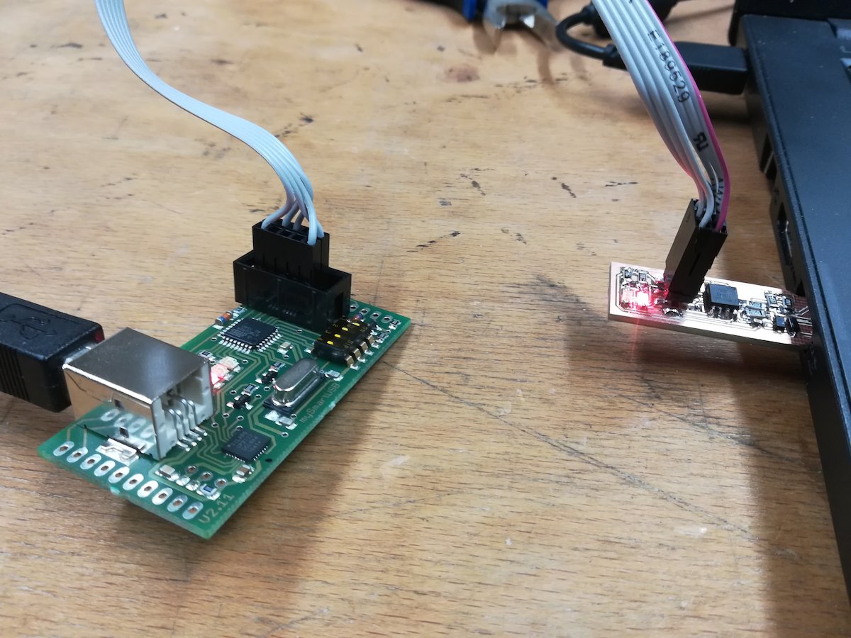
Programming
The last missing part is to program the ISP to be an ISP itself. For this, we use a mySmartUSB MK2 and avrdude. I only have Linux available on my machine, but Brian's original tutorial has additional instructions for Mac and links to instructions on how to do it on Windows. Get the firmware. In the provided makefile, change the line
PROGRAMMER ?= usbtiny
to
PROGRAMMER ?= avr910
provided you also use the mySmartUSB MK2 programmer.
If not, find out what avrdude calls your programmer board and use that.
Additionally, I had to substitute -P usb with -P /dev/ttyUSB0, because that's the USB port that the programmer was plugged in.
To find out which value to use here, run ls /dev | grep USB before and after plugging in the programmer into your PC; the additional entry should be the correct port.
Now, build the firmware by calling
$ make
in the directory where you unpacked it.
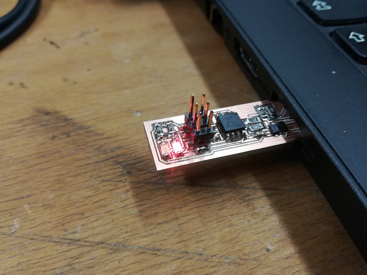
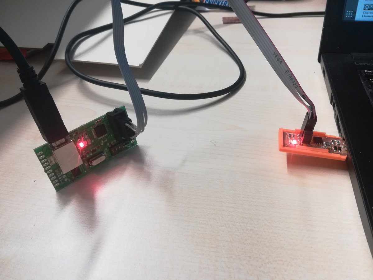
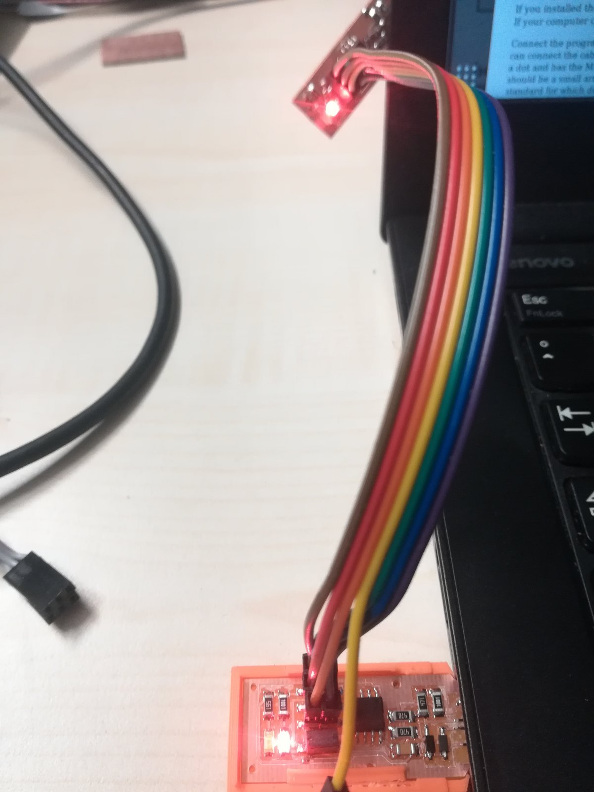
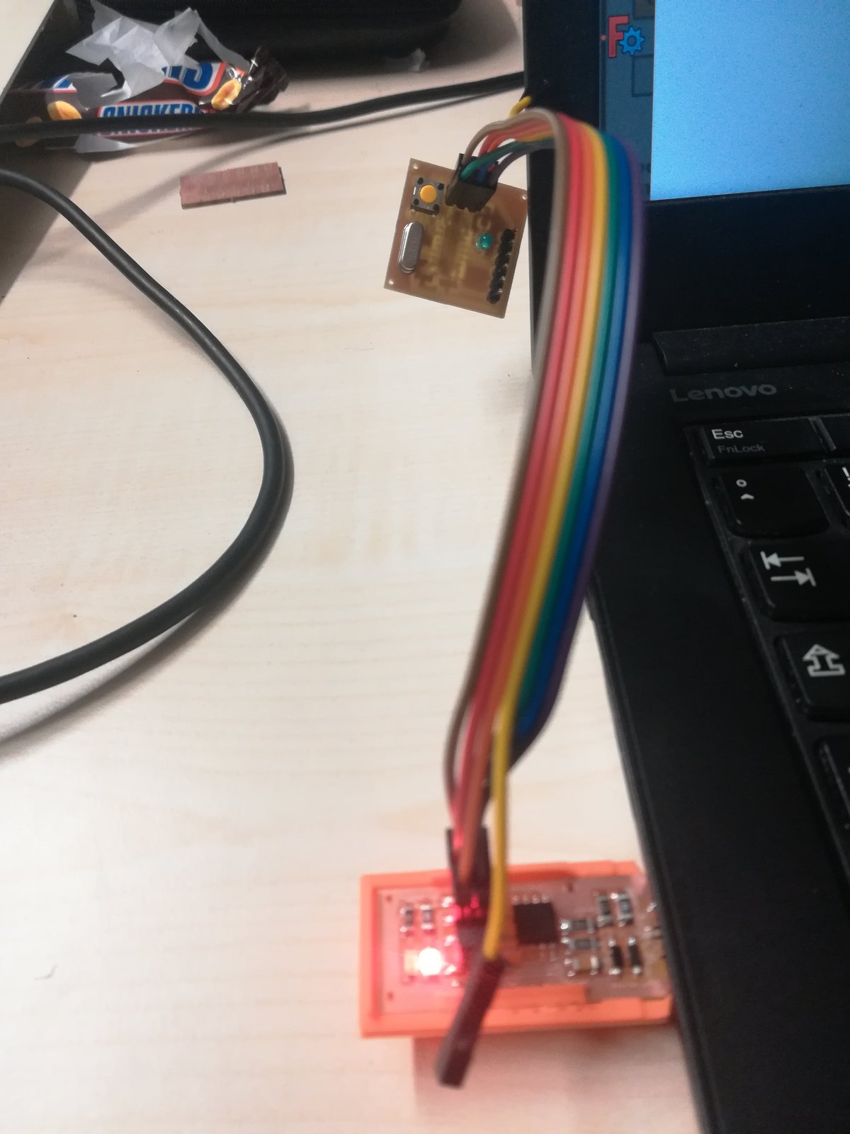
Plug the board you produced and the programmer into your PC, and connect the board with the programmer. The red LED should light up as the board is connected to power.
Make sure to connect the pins correctly, i.e. pin 1 on the programmer with pin 1 on your board, etc. Then run
$ make fuses
Now it's time to test if our board is recognized as a USB device. Unplug the programmer and the board, remove the connection between the two, and plug the board back into your PC. Run
$ lsusb
in your terminal.
If a "Multiple Vendors USBTiny" appears, it works!
Congratulations.
If not, you can check for errors with dmesg.
Oh no, it's not working!
Now, for me, it didn't work.
dmesg would give me errors like
device not accepting address 36, error -71
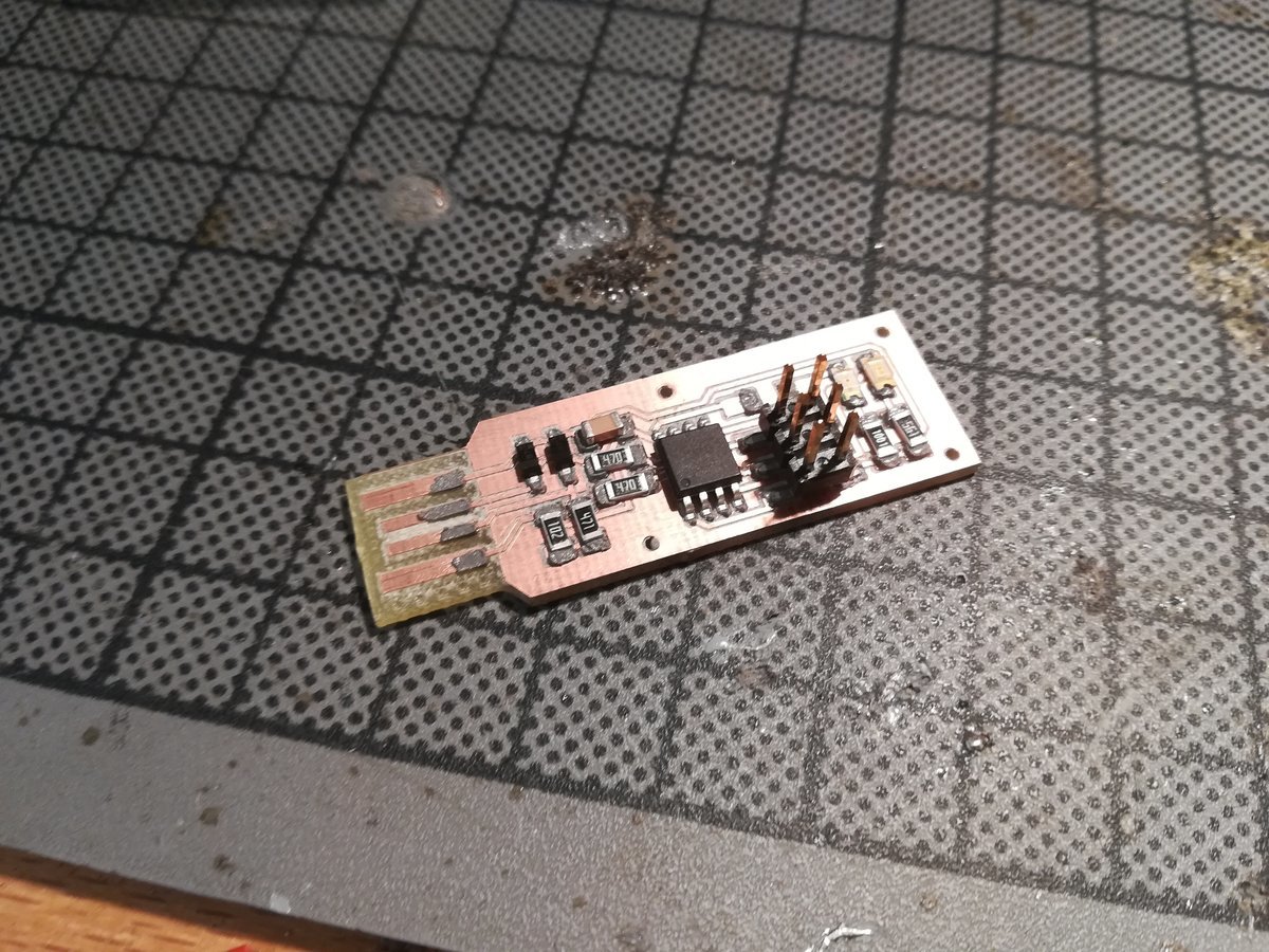
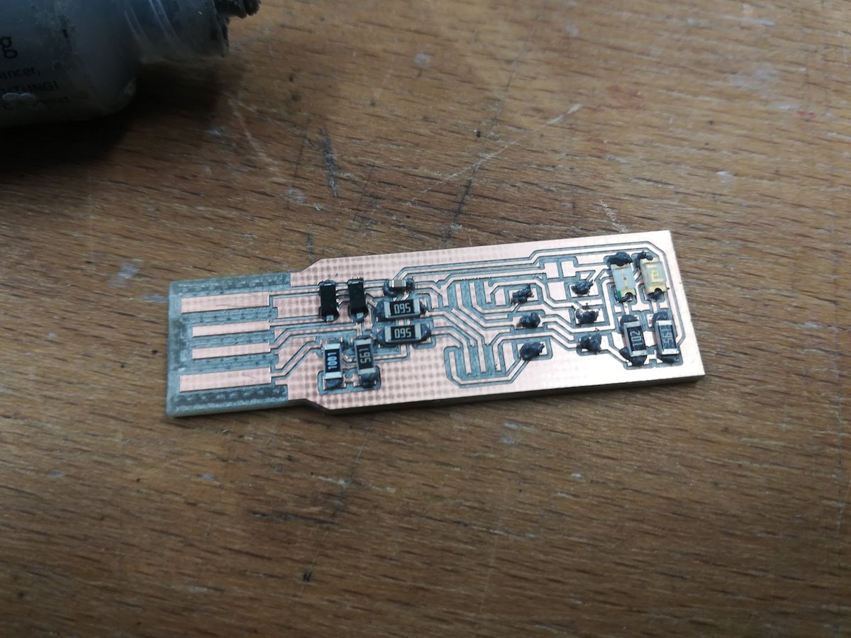
Now what? I used a multimeter to check for shorts, but found none. Since I could program the board without problems, there must be something wrong between USB port and micro controller. So I frankenhacked my board and put smaller resistors in. And voilá, it works!
The last thing we have to do is to remove the reset fuse, which disables the reset pin and turns it into another GPIO pin. Afterwards, the board will not be programmable anymore, so make sure it was working beforehand! To irrevocably turn your board into a programmer, run
$ make rstdisbl
Also, remove the solder from the jumper to break the connection between VCC and the programming pin on the ISP header. Finally, we make sure our board actually works by programming another board with it. Since my first board didn't work, and I wanted one that is properly made, I milled & soldered a new one, and programmed the hacked board with the new board.
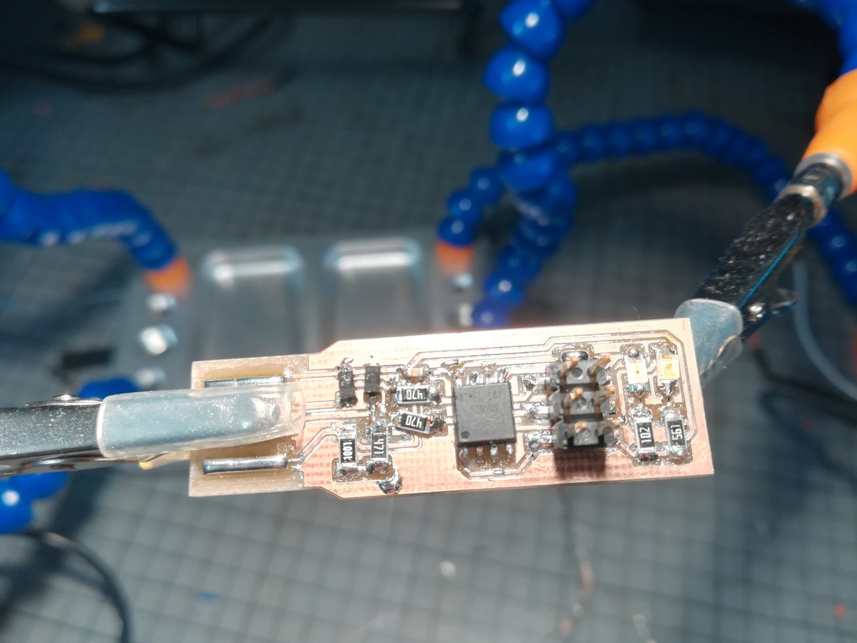
Soldering a new board with the hot air gun
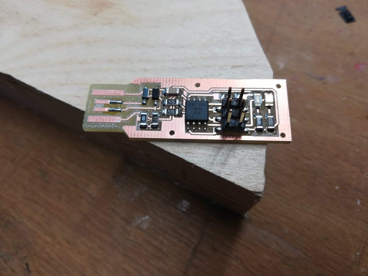
I've added some small modifications to the board design & layout: I switched the capacitor for a bigger one and exchanged the solder jumper for a pin jumper, so it's easier to bridge/unbridge it. Additionally, I added some holes and specified the board dimensions in such a way that I can make a case for it during the 3D printing week. The EAGLE files in the download section describe the modified board.
For the new board, I tried hot air soldering with soldering paste. First, I made a stencil out of 240g/cm^2 paper with the laser cutter. To create the stencil, I exported the "tCream" and "dimension" layer in EAGLE as a PDF file and imported it in Inkscape to prepare it for the laser cutter. It is important that in the document properties, the measure & display unit is set to "mm", otherwise the stencil might have the wrong size. Then, I used double sided tape to fix the board, positioned the stencil above the board, applied the solder paste and removed the stencil. After stuffing the board, I used a hot air gun to solder all components at once. Pay attention not to overheat your components when using the hot air gun. Also, don't burn yourself, it is really hot. After inspection with a multimeter and a magnifying device, I found that the resulting connections are indeed very well done. I think that making a stencil, using solder paste and the hot air gun is a very easy, fast, and practicable method to solder lots of small SMD components. I will definitely use this method in the future to solder my boards.