
This work is licensed
under a
Creative Commons
Attribution-NonCommercial-
ShareAlike 4.0
International License.
These week's goals are:
Demonstrate workflows used in network design and construction.
Implement and interpret networking protocols.
The requirements are:
Described your design and fabrication process using words/images/screenshots.
Explained the programming process/es you used.
Outlined problems and how you fixed them.
Included original design files and code.
Types of Communications:
Asynchronous Serial Protocol
I2C
SPI
USB
The simplest options are Asynchronous and I2C . A network is a set of connections between several elements. This week we have to use one of the computer network types to make two boards, one is the bridge node and one is tree node. The goal is to make the boards communicate. I will work with the asynchronous boards.
For this week's assignment I've decided to go use the I2C communication protocol. In order to further understand the concept, I have followed the I2C tutorial on Sparkfun.
Find below my notes on the reading:
I2C stands for inter-integrated circuit and is only intended for short distance communication. Why pick I2C over a regular asynchronous serial bus interface?
1.Asynchronous protocol have no clock data so the data rate between the boards that have to communicate needs to be setup beforehand.
2.Also asynchronous serial ports only work smoothly when trying to communicate between ONLY two devices. This is because the two devices must try to use the same line at the same time. This is also known as bus contention.
As a reference, I followed the steps of the following alumni:
Katerina Labrou.
Edgar Aguilar.
Sam Calish.
Hanna Lakk.
For the RGB led reference, I used this one http://fab.academany.org/2018/labs/fablaboulu/students/peetu-virkkala/Week12.html.
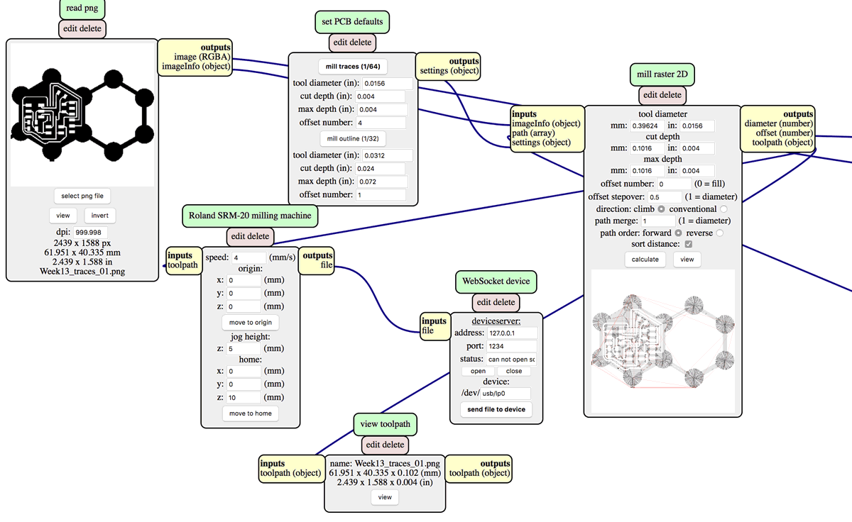
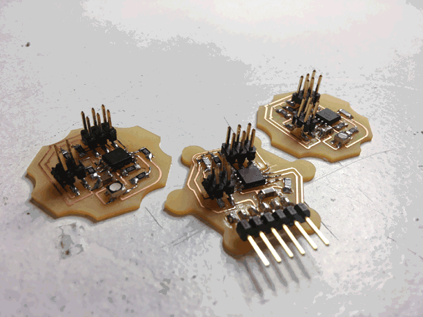
During this week, I did not have any issues when generating the g-code for the master board as seen below.
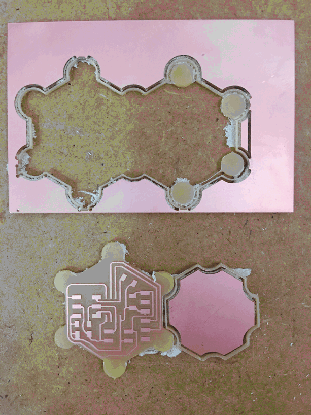
However, I did encounter two overlapping paths in the slave boards. Because during that week I had to travel to my city, I was able to get an affordable soldering iron and set up a simple station at home. This also meant that I had to be particularly careful when scratching out and soldering the overlapping paths since I did not have access to a multimeter for a while.
As I was working on the output assignment, I had already had the following issue with the custom board outlines. When I milled the outlines of the master board, I saw that the milling machine had traced a stroke with a cut on each side instead of a single one. It was a shame because the cut-out part ended up being too thin and it broke when I detached it from the sacrificial layer. Not only I was not able to insert the slave boards in the cut-out space but I wasted almost half of a PCB. Thankfully, I was able to see what I had done wrong. When working on the outline Design in photoshop, I should have filled with white the space outside the board. I did that with the slaves and the milled boards turned out fine.

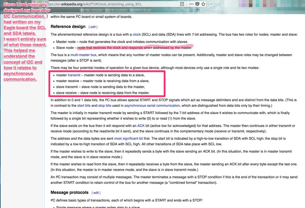
This week, Neil Gershenfeld's randomizer picked me. When he saw my boards, he suggested that I used the asynchronous communication protocol instead of I2C since the latter often entails more complications. The following points outline the relationship between the IC2 and a Asynchronous communication protocol.
SCL - sends clock data to slave. Therefore it corresponds to TX.
SDA - receives data from slave. Therefore it corresponds to RX.
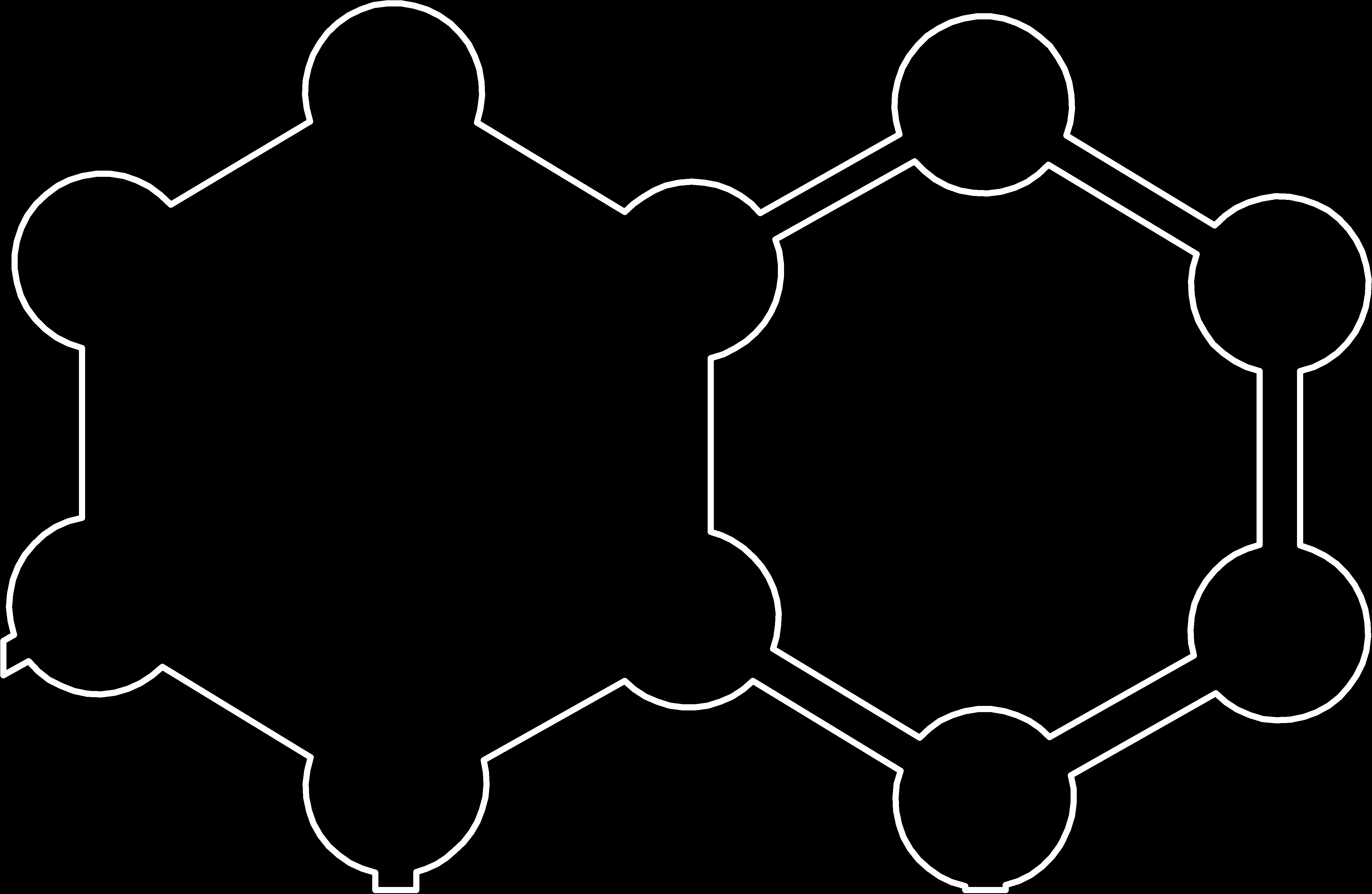
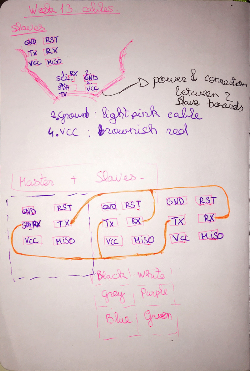
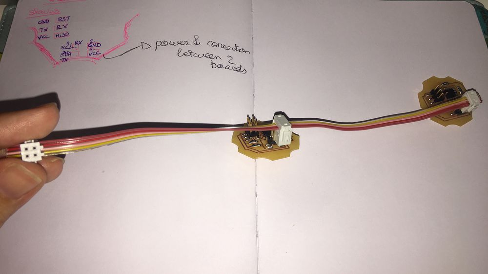
Since I had originally designed my board for I2C Communication, I had written on my Eagle board the SCL and SDA labels. This helped me understand the concept of I2C and how it relates to asynchronous communication. I also used the Serial Software library that I had previously used during Week13: Applications and Interface Programming. I used the pin-out diagram to understand how to wire the boards together and drew a sketch to visualize it better:
SCL - receives clock data from master. Therefore it corresponds to RX.
SDA - sends data to master. Therefore it corresponds to TX.
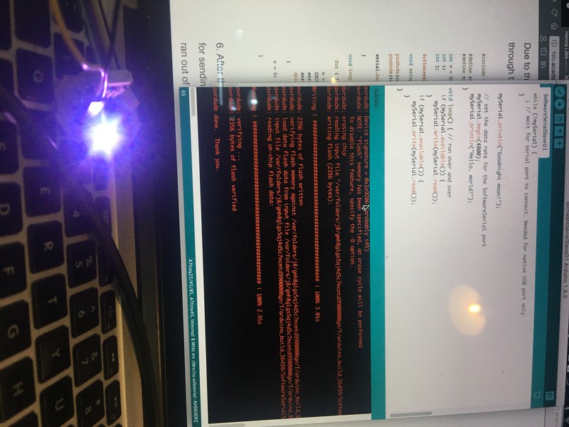
I first tried to power one of my slave boards through the master board which was connected to the computer by an FTDI cable. Unfortunately, I didn't connect the jumper wires properly and this created a short-circuit. I did have to rebuild from scratch by second board. The issue was not fixed by simply replacing the microcontroller . But thankfully I did manage to program one of the slaves.
A couple of considerations when programming the RGB led:
I followed the steps of this Jack O'Lantern Instructable and complemented it with Peetu Virkkala's documentation.
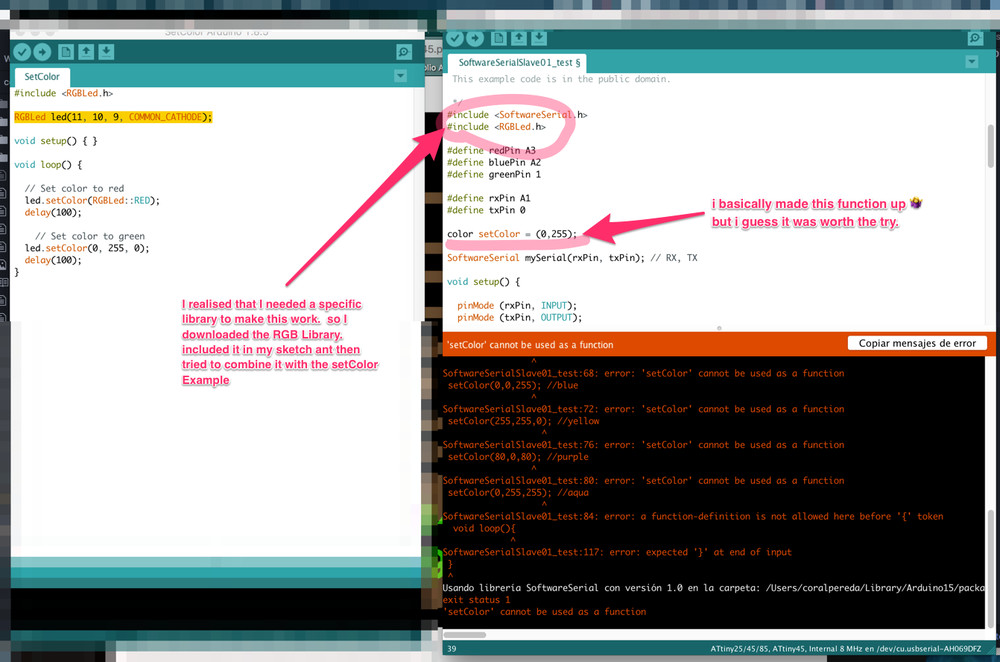
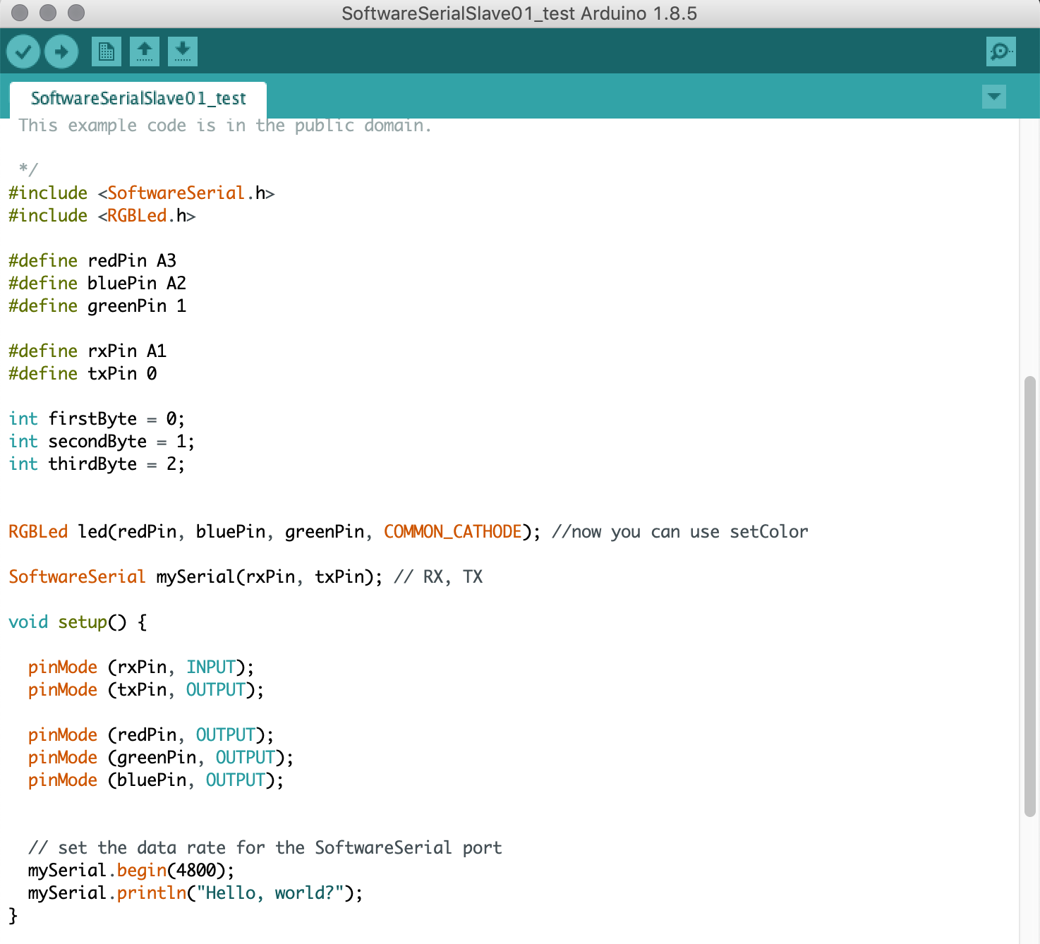
I installed the RGB library and included it.
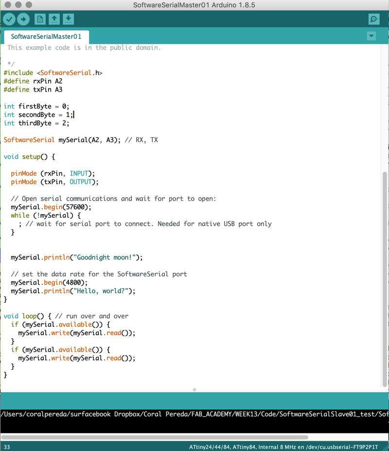
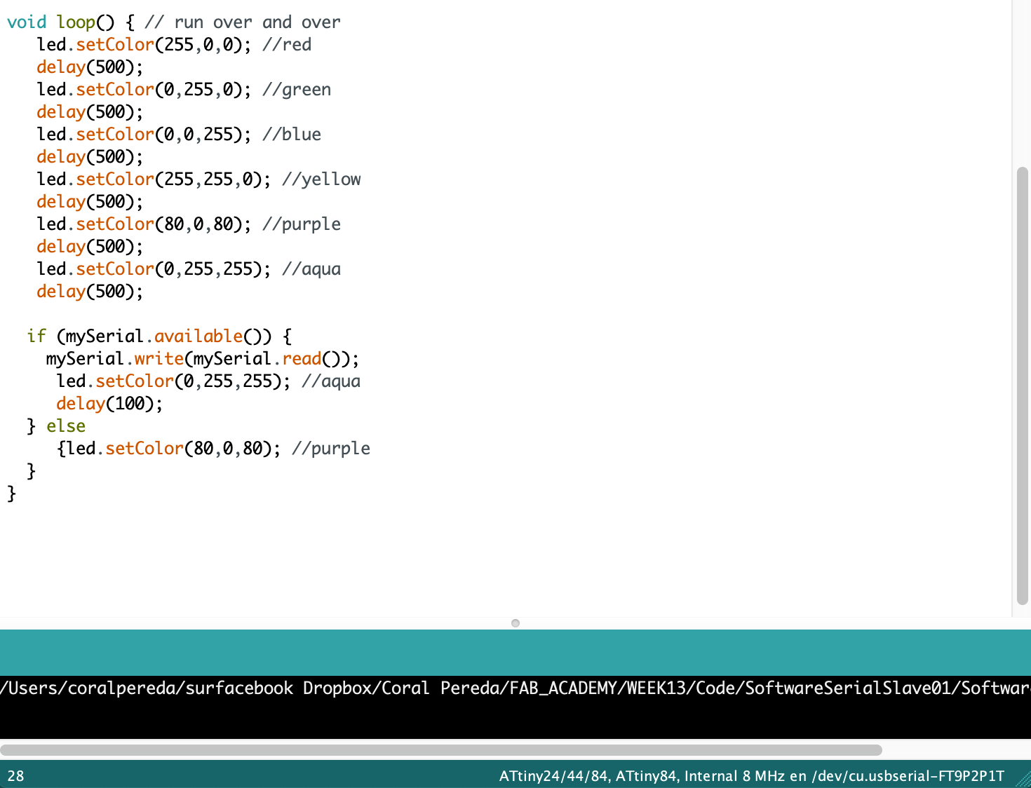
Then based on the RGBLed library example, I combined it with my own code based on the Software Serial arduino example.
Then I decided to power the Slave boards separately from the master board to avoid confusion. I did so by connecting them with 2x2 connectors and then using jumper wires to connect one of the connectors to the GNC and VCC of an FTDI Cable.
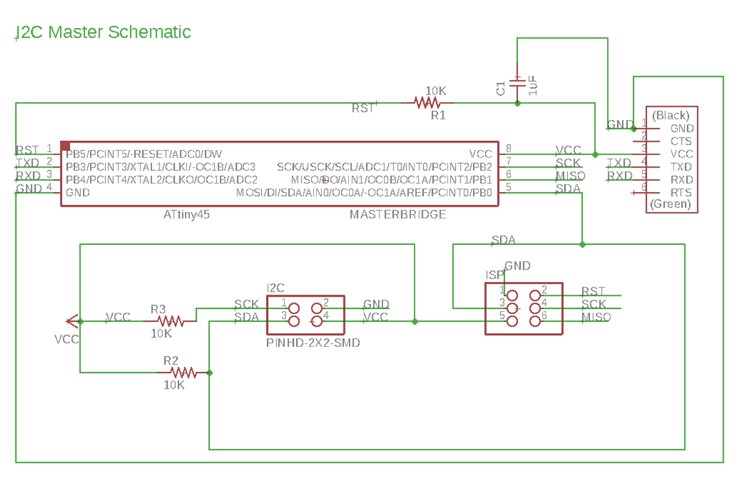
Master Eagle Schematics
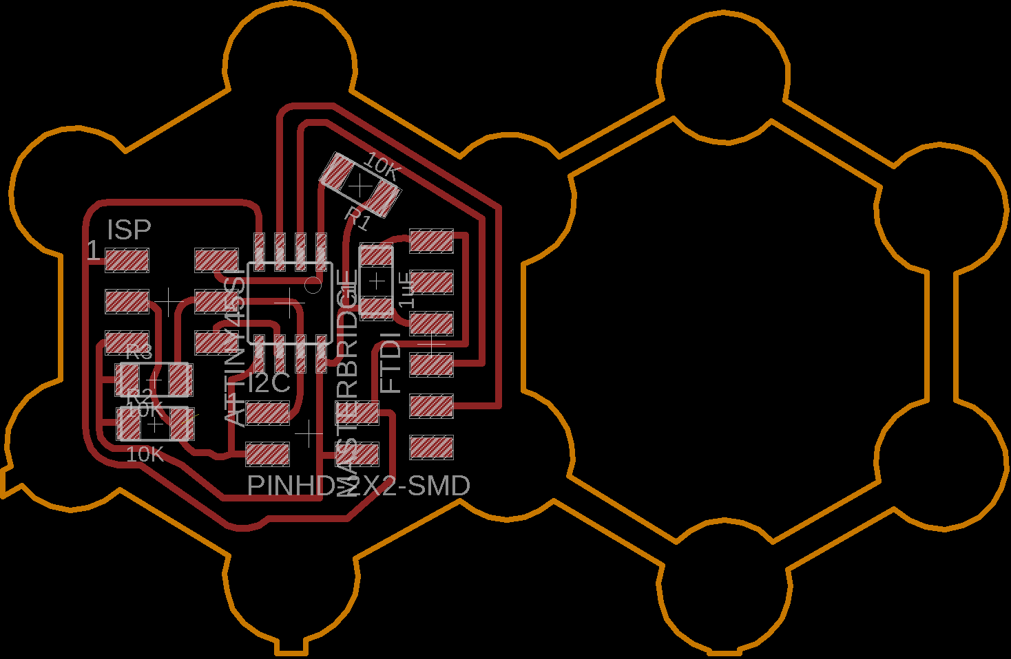
Master Eagle Board
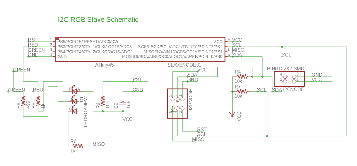
Slave Eagle Schematic
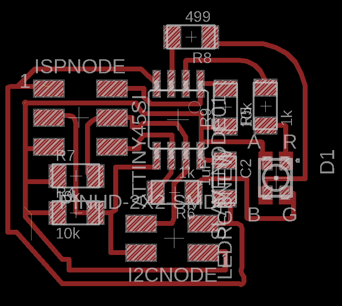
Slave Eagle Board
Master Code
Slave Code