Week 06 – [Electronics Design]
Dates worked: [February 25 - March 3th, 2026]
Time invested: ≈ 55 hours (spread over 7 days)
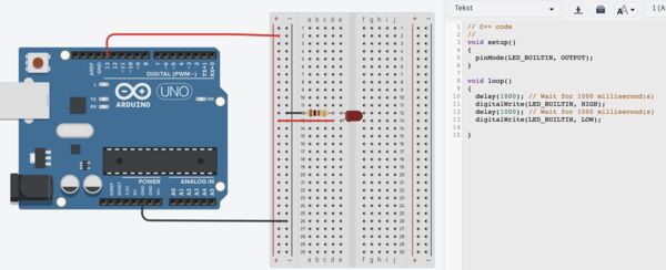
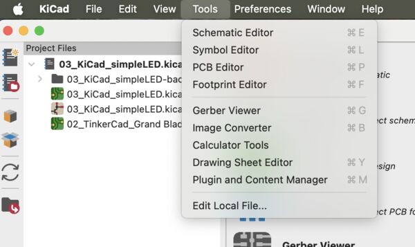
Simulating a simple circuit in KiCad
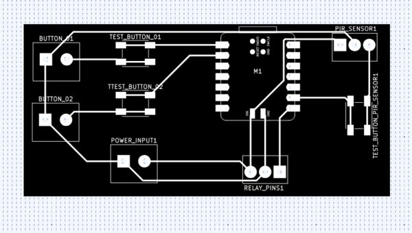
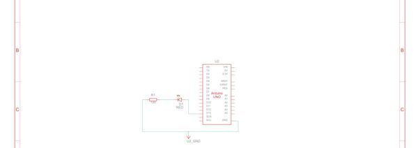
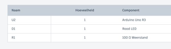
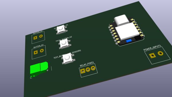
Final design
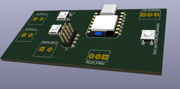
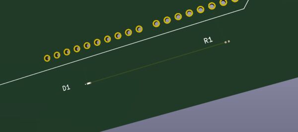
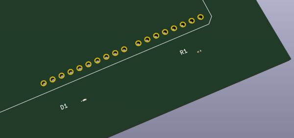
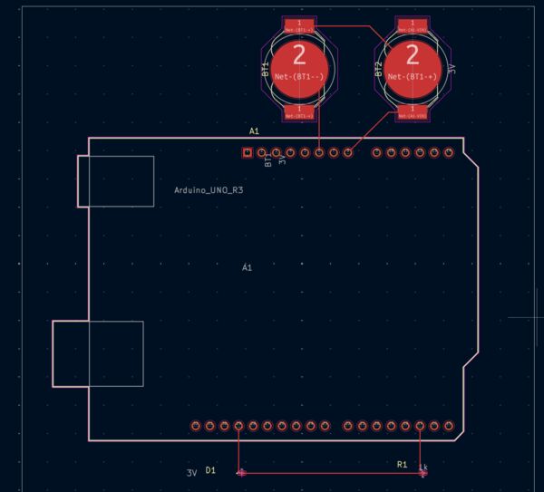
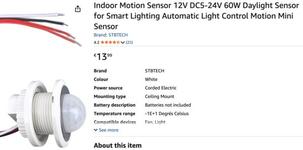
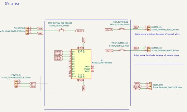
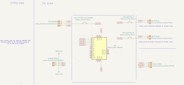
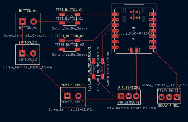
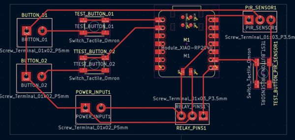
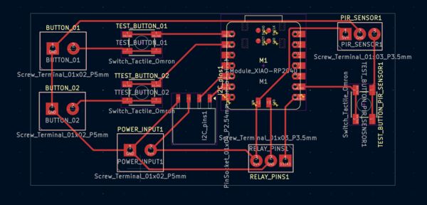
This board embeds the XIAO RP2040 microcontroller. It has local input via PIR motion sensor header and local output via relay control pin. External communication is enabled via the XIAO's USB & I2C
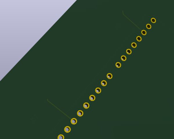
Based on Gerber files
Quick summary of my week
This week I learned to treat ERC/DRC errors like compiler warnings and iterating schematics/PCB like refactoring code. I designed (and verified as fabricable) a 5 V development board around the XIAO RP2040 that reads a PIR motion sensor, controls a 230 V lamp via relay, and exposes I2C + USB for future external devices; directly inspired by my home LED light project. The process felt jumpy at first (wrong footprints, power flag mysteries, track width fights), but talking to Henk and methodically fixing one DRC cluster at a time turned it into a compile/run cycle. Adding the I2C header late felt like a bit exciting so before the deadline 
I also ran several small simulations: a SPICE model of an LED in KiCad to visualize its forward voltage curve, and real-time transistor behavior in EveryCircuit on my phone — watching a lamp brighten through variable changes in a debugger.
Of course now that the week is at its end I would have liked to create more, more fun stuff ... but that's life at the moment
Remark: Although I have added links to subpages .. I have added tabs below to also directly access them
Requirements & objectives
This week's assignment was described on the Fab Academy 2026 assignment and assessments page as:
Group assignment:
- [x] Use the test equipment in your lab to observe the operation of a microcontroller circuit board (as a minimum, you should demonstrate the use of a logic analyzer) --> see "Day 2 Thursday"
- [x] Document your work on the group work page and reflect what you learned on your individual page
-> No shared group page exists; work is described here + cross-linked to Heleen Emanuel and Remco van 't Veer
Individual assignment:
- [x] Use an EDA tool to design a development board that uses parts from the inventory to interact and communicate with an embedded microcontroller
-> Designed from scratch in KiCad using Fab inventory parts (Seeed XIAO RP2040 as embedded MCU, screw terminals, diode, headers). Board includes local input (PIR motion sensor header), local output (relay control pin), and external communication (native USB + added I2C header for SDA/SCL) and verified via Gerber
Learning outcomes demonstrated
To help myself and whoever is reviewing me, I'm pretty sure our group has demonstrated the learning outcomes for this week. Again, as we don't have a group page our work has been described here and on our personal websites:
Regarding my individual assignment, I: - Evaluated multiple EDA tools (Fritzing, Tinkercad, LibrePCB) but chose KiCad for its power and Fab Lab compatibility - Followed full workflow: schematic --> ERC --> PCB layout --> net classes tuned to Waag rules --> routing --> DRC --> 3D view --> Gerber export --> online verification - Designed board with embedded XIAO RP2040, local input (PIR header), local output (relay pin), external comms (USB native + added I2C header) - Understood and applied key concepts (flyback diode, power flags, net classes, clearance rules) through trial-and-error + forum/YouTube research - Ran circuit simulations (KiCad SPICE LED I–V curve, EveryCircuit transistor saturation demo) to build intuition for analog behavior
My week – how it actually unfolded
Day 1 - [Wednesday - Regional / GLobal session]
Started this new week around 12:00. The first part of this day I described in week 05.
Henk showed us a video of the concept of MCP (Model Context Protocol) interfaced with Blender; can be viewed as aa layer between AI and API's. It's much more than just asking AI to generate a model for you. Basically, in the video, we saw how Blender's interface was used; like someone taking over your keyboard/mouse.
This also reminds me of the recitation about AI from last Monday. Tutor César García also showed the concept of MCP whereby MODS was integrated (content is not in the slides but in the video around 28 minutes)
Remco then points us to a podcast "Shell Game" in which a person starts a business with only AI workflows.
Regional session

Like last week we all showed our work in around 2 minutes.
Summary
Group Hisar Fablab
Poyraz Ozzengi kicks off and tells about using several Bamboo printers in the lab. -> his page. Can Ortanic takes over. He also changed the nozzle to a 0.35mm diameter. -> his page. Back to Poyraz he shows that they did a lot of infill tests. Well documented. Poyraz tells about his personal assignment and also shows how he scanned .
Mehmet Bener: used OnShape to create a sphere inside a small building/ temple. He also scanned his head and printed it. -> his page
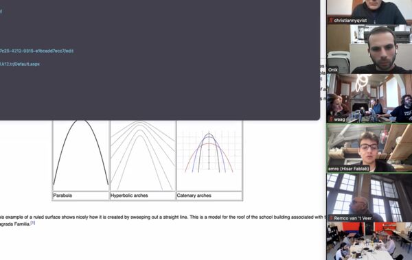
Emre Dayangac: used OpenScad to create his object. Inspired by Gaudi he created a similar kind of object using code with https://threejs.org/. Then sliced it and printed it. He shared a link bout it https://eschermath.org/wiki/The_Geometry_of_Antoni_Gaudi.html#Parabolas; see his page
Emre's inspiration
Group Brussel
Michel Osée: Also printed the test object we used and used OpenScad to create additional tests. Created a very cool object (we want a video of this) and scanned a printed chair (also using Ferret as we did). -> his page
Jonas Grimaud: Used the same test as we did. Had some problems with printing (probably needs a smaller nozzle). Used OpenScad to create a rotor inside a rotor; a kind of pump. Also scanned using CrealityScan -> his page.
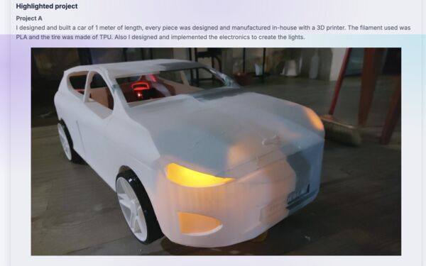
Fabio Coelho: Used Fusion to create a cube model; nice. Used Gravity sketch to model this scanned object. He showed VR glasses; did he use those? Also used other scanners. Shows his little car that he printed -> his page.
** Group Aalto-Fablab
Tomi Nieminen: Showed color printing; nice. Scanned a brain model. Already used MCP interface with Blender. Had to start learning Blender as well. -> his page
Group Amsterdam
Heleen Emanuel: Switched to Blender as well. -> her page
Remco van 't Veer: Created his object in OpenScad. He used his own printer; also experimented with PET which he found very stringy. -> his page

Remco's work
Group Armenia (Onik)
Mariam Daghbashyan: Scanned person on a chair. Experimented with temperature first and did the same printing test as we did. The print in gold is beautifull. Created eyes for on her mouse -> her page
Henk's remarks to everybody: when you are using a new machine introduce it; handy for the global evaluator
Global review
Neil kicks off with Rodrigo Zárate ... He shows a very cool print of a car.
Wauw! This is work that he did before. Ohad Meyuhas (one of the teachers about 3D printing from last week) discusses topics regarding how he connected all the components together. -> his page
Next up Ardravedi K. from Kochi, India. Her "Soul Sync" idea looks very nice. No comments because she documented everything very clearly -> her page
Next up Rocio Milagros Maravi. Her final project idea: Low Cost Smart Culture Chamber for Trichoderma .. I asked Grok to translate her idea and her idea is to "The project aims to democratize access to this biotechnology by creating an economical, easy-to-assemble chamber so that local labs, producer associations, small CITE Productivo Madre de Dios staff, and communities can autonomously grow and maintain fungal cultures without depending on imported or costly equipment.".
She shows 3D tests that look very rough.
Whole discussion takes place about what she used, how hot the filament was ... From her website I see that she used a CARMEN printer. She also used other printers and the output is much nicer. Neil is happy with the group page. -> her own page.
Next up Emily Noor -> She takes the course from China with her husband Timothy but they are from Indonesia. One of her ideas is to create device to answer Kahoot like quizes.
Neil says this should be possible. For her assignment she created her own hinge. -> her page
Next up Angela Henderson. She has a lot of ideas including "Solidarity City Builder".
It triggers Neil to show the work of a collegue that show interactive map of a city via video projections (Neil confirmed he refers to https://www.media.mit.edu/groups/city-science/projects/) -> Angela's page
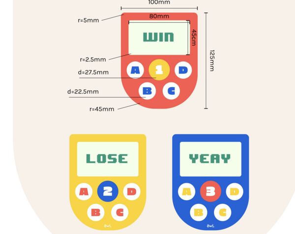
Next Kamil Gallardo Toledo. Currently student batchelor in Mechatronics. His idea is to create some kind of electronic punching bag; uses memory game as an example. Neil refers to the use of conducting fiber as a possible sensor. Jani Ylioja refers to a project from Petra Rutanen from 2023 that did something similar. In the chat there is also refered to https://fabacademy.org/2025/labs/oshanghai/students/shuijiao-li/projects/final-project/ as a simlilar project. The sensor they are talking about is a piezoelectric sensor: is a device that uses the piezoelectric effect to measure changes in pressure, acceleration, temperature, strain, or force -> Kamils page
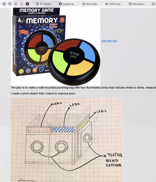
Kamil's inspiration for the punching
Afterwards we had an open session whereby students could show/ share their work/ ideas.
General remarks by Neil: - Pushing/ describing your work has to be part of the workflow; not after the work has been done. Document as you work otherwise you'll not make the class, you'll be running out of time otherwise - Glues and sprayed not really necessary; keep the bed clean (acknowledged by Aristarco Cortes). For scanning maybe (according to Ohad Meyuhas) - Open time is meant for this week's assignment: success and failures
Note
Note to myself: do a further design of final project; like the subsystems and how I think I should make them.
Note to myself: Use Blender to start make a render for my final project.
Note to myself: if using AI maybe switch to microPython just for prototyping?
Global class
Subject for this week is electronics design: basically "Design and simulate a circuit board... in 2 weeks you will produce the board that you design this week"
Sources given by Neil are:
- Tutorials
- Subjects/ links
- Adrian Torres; student from 2020
- Ani Liu; student at MIT Media Lab
- Kai Zhang --> created his own tool/ code to divide electronic components on a board
- The art of electronics - Paul Horowitz - according to Neil handy book with tips and tricks
Neil mentions: "Today you'll see the valley, next week you'll walk through it"
To be honest Neil introduced the electronic components in high speed (well basically everything) so I did not have time to make notes on all of them I have worked with electronics before (and really in a very amateur manner) so I had an idea of most of them. Below are some comments that Neil made that stuck with me; like new to me and/or forgot how it worked:
Electronic components
- Ribbon Cables are handy because you can stripe them down to less if you want to and they stay nicely together
- IDC connector = electrical connector; really useful as you open it, place the ribbon cable inside, close it and then voilá the wires are connected
- Wire Gauges: code 28AWG refers to the American Wire Gauge standard for wire thickness. Thinner wires (higher gauge) are common in prototyping but handle less current. So for my designs the trick is to choose wire gauge based on my current needs (to avoid overheating)
- Resistor: I = V/R (that one I remembered) but Neil used a metaphore .. Voltage is the height above ground; I = current is how much is flowing. Resistor's unit is Ohm; and in datasheets the tolerance of a resistor is also mentioned
- Capacitor stores charge C=Q/V ... Blocks AC current but let DC currents through. Typical values are micro Faret. So to control big motors you use big capacitor.
- Inductor is the opposite of a capacitor. It blocks DC but allows AC to pass
- Crystal: used for precise timing in circuits (e.g., clock signals for microcontrollers).
- Diode: Has two sides: anode (positive, receives current) and cathode (negative). Allows current in one direction only, protecting other components from reverse voltage.
- Zener Diode: A special diode used to regulate or "clip" voltage to a specific level, preventing overvoltage.
- LED (Light Emitting Diode): Similar to a diode but emits light. Always pair it with a resistor to limit current and prevent burnout. DigiKey lists over 26,000 LED options.
- Transistor BPOLAR: they always use current
- MOSFAT transistors: there are 2 kinds N and P / Gate sets a resistance between source and the drain
- Power = I * V = I squared * R: determines battery life, heat generation, and risk of overheating (e.g., in transistors). Aim for low resistance (R) to minimize power loss.
- Voltage regulator: Converts input voltage to a stable output (e.g., 3.3V). When gate voltage drops, it can behave like a resistor ..
Common design pitfalls
- Grounding Issues: A frequent mistake is not connecting all components to a common ground, leading to unstable or noisy circuits.
- VCC: Stands for voltage at the common collector, typically the positive supply voltage.
- Design Rules: Yes there are rules . Check how close components can be near eachother, how close traces can be. Milling machines can't produce traces finer than 1/64 inch (about 0.4mm). My PCB layout must match the fabrication process
- ERC (electrical rules check): Verifies all connections are made correctly and without errors, like a compiler check in software (looks like unit testing)
How to design
- Simplest way is to draw it by hand; In early days, designers used tape layouts and faxed them for production.
- Tinkercad/ virtual breadboard: user-friendly for beginners; simulates breadboarding. Fun for quick prototypes, but skip if you need advanced features.
- KiCad is loosely affiliated with CERN. Very powerful; open source project; You first need to first upload symbols and footprints of those. Like Kris has done for all the fabacademy components --> his work
- Neil shows couple of libraries; if you need newer parts then you start of with your own library
- Simulation is increasingly important. WokWi let's yo pick a processor then it has an emulator; load the code; at components. Has pretty much al the parts that we use. But WokWi does digital simulation not analogue.
- Falstad: Another digital/analog circuit simulator; supports mixed-signal designs.
- You can also mix true digital and analogue. Pablo mentiones Cirkit Designer. This is another simulator that has many more boards and modules.
- SPICE. For simulating integrated circuits (ICs). KiCad can export to SPICE for analysis.
Testing and Debugging
- Power Supply: Useful for gradually increasing voltage during testing to avoid damage.
- Multi meter: to measure voltage, current and resistance
- Logic Analyzer: Captures and analyzes digital signals.
- Osciloscope: measures analogue in time
- Salea: For both analog and digital troubleshooting.
Special mention by Neil of Adrian Torres's work from 2020 on debugging.
And, March 8th US switches daylight savings time!!!
Invested time: 11 hours
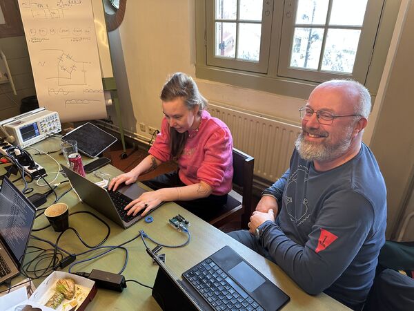
Day 2 - [Thursday]
Started around 07:15 (cats were up early). Worked on documentation and went to the Waag.
Fix bash script
Assignment from Henk based on my week 02 documentation is to be able to run my shell conversion scripts (video/ images) in a way that I can run them without calling bash first. According to the internet calling my script like ./<name of sh file> is enough. But without the . it does not work. I asked Grok about this because I couldn't find it online that fast.
So actually I now just call my scripts with bash first using ./<script.sh>. This only works because the first line of each script is #!/usr/bin/env bash (which is already the case by the way).
Local class
(Like the global class I've written this part based on my notes but in the past .. again I've written down what stuck to me the most).
Erwin Kooi - student 2020 was our tutor for today.

His presentation - see "Electronic design". Using this he reviewed the most important electric components (thank you for that!)  . But before that he got back to the basics
Voltage, current & power
He used a nice analogy to explain voltage and current.

So the voltage is the pressure by which the electrons are moved through the wires/components. The amount of electrons is equal to the current (I). Rule is that in a electrical circuit the sum of all voltages is equal to 0. The current in equals the current out (as electrons are not lost).
To demonstrate the effect of voltage Erwin referred to a video of a guy that hooked up 400 car batteries together. So the voltage is 12V (low right?) but the current is enormous. The message is that even with low voltage you have to watch out.

Note
Because Erwin told us about the analogy of voltage as pressure ... it was now clear to me why the guy could stick his hands between the clamps and not get shocked. The pressure was "only" 12V. Erwin gave us a general rule that you should keep a distance of 1cm per 1000V to prevent current transfer. As you can see in the image

there is far more space here then is required for 12V. But now I also understand that people near power station should not point their finger as they can be hit by current; reason is that the voltage is around 230Kv ... so do the math. Once the current starts to flow then it flows.
Power!!! (in Dutch: vermogen). Can be seen as the unit of labor/work and is noted in Kwh (kilo Watts per hour) = voltage (V) * current (I). Getting back to the falls, they probably deliver the same power.
Electrical components
Resistors (R) - One of the most important and frequently used passive components. - They "rem" (slow down/restrict) the flow of electrons, limiting current. - Water analogy: A resistor acts like a narrowing in a pipe, reducing water (current) speed and causing a voltage drop (pressure drop). - Two main types: through-hole and SMD (surface-mount), each with their own color/band coding system. - The gold (or silver) ring indicates tolerance (accuracy of the resistance value, e.g., ±5% or ±10%).
Capacitors (C) - Act as a storage tank for electrical charge. - Key formula: C = Q / V (capacitance = charge stored / voltage). - Q (charge capacity) comes from the datasheet—it's the measure of how much the capacitor can store. - In DC circuits: behaves like an open circuit once charged (blocks steady DC after initial charging). - Placed behind a battery: The positive plate charges up until the capacitor acts as an open connection. - When power is removed, it holds charge for a while (useful for backup or smoothing). - In AC circuits: acts like a resistor - Usefull to debounce switches/buttons: When pressing a switch, mechanical contacts "bounce" (rapid on-off), creating noisy voltage transitions. A capacitor across the switch absorbs these bounces so the microcontroller sees clean "on" or "off" signals instead of rapid flickering.
Diodes
- Allow current in one direction only (anode to cathode).
- Material determines properties, including color in LEDs.
- Forward voltage: Minimum voltage needed before the diode conducts significantly.
- Forward current: Maximum safe current; always calculate and add a series resistor for LEDs to limit current.
- Erwin gave an example: To drive an LED, compute resistor value using Ohm's law: R = (V_supply - V_forward) / I_desired. If the exact resistor isn't available, choose the next higher value for safety (lower current) or lower if you need brighter light (but monitor it's heat).
- Bridge rectifier (a what? in Dutch "diodeburg" ): Four diodes arranged to convert AC to DC (nice ). Add a capacitor after the bridge -> smooths output to get a flatter DC voltage.
- Special type = Photodiode: allows current to flow when light hits it (used in sensors).
Inductors / Coils (L) - Opposite behavior to capacitors. - Create a magnetic field when current flows (used with DC). - Usefull to create "pull" something (relais), rotated something (motors), and when 2 are used transform voltages - Key feature: Magnetic field "wants to stay alive"—when voltage is suddenly removed, collapsing field induces a reverse current, which can damage components. So as a solution add a "flyback diode" (often across relay/motor coils) to safely route this reverse current.
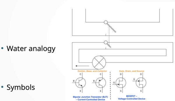
Transistors (Q) - Used to switch current on/off OR(!!) regulate it partially (analog control); wauw - Protect microcontrollers: Example, use a transistor to let a low-power pin switch a high-power 12V load. If miswired, worst case is smoke, but MCU survives (unlike direct connection). For true isolation (high voltage/current separation): Use a relay (electromechanical switch). - Other idea is that you can drive multiple loads: Example, of 10 LEDs. You might need 100mA total, but the delivers a maximum of 50mA. Then a transistor pulls current directly from battery/supply, controlled by tiny MCU signal.
Appearantly there are 2 types: Bipolar and MOSFET. I must admit that I did some more digging as I found this one difficult to understand. See my conversation with Grok about this.
I have used part of it's output and altered the slide of Erwin for this.
I still found Grok's explanation difficult and asked for a water analogy. Hmmm ... why is it so difficult to understand. As suggested I asked for Wokwi examples. I tried a few links but I don't think they are correct.
I leave it for now and remember what Erwin said:
- Binary Junction Transistor: use it to switch current; bipolar means: a small current can amplify a bigger currrent
- MOSFET: Voltage-controlled: Small gate voltage controls resistance between Drain (D) and Source (S). A small voltage can drive a larger voltage
Anyway, that transistors could regulate was new to me. I thougt they could only really switch
Microcontroller (MC) vs. Microprocessor
- Microprocessor = core computation engine (ALU + memory).
- MCU = Microprocessor + integrated peripherals (timers, ADCs, UART, I2C, SPI, GPIO, etc.).
- Controlled via registers (memory-mapped I/O).
- Many options: Choose based on capabilities, peripherals, power, and price.
- Example: RP2040 (~€4) vs. cheaper alternatives (~€0.20).
- Factor cost into designs—cheaper parts scale better for production.
Measurements
Multimeter: does require some time to take a measurement; so with big fluctuations it is not very suitable. It actually only measures voltage(!). It measures current via adding an internal resistor
Note
Tip when turning of; always return to voltage setting before detaching the wires = leads.
Henk demo's a smart version = turn it on and it says "auto". The device figures out what you want to measure. BUT it is therefore very slow; enoying. So yes, the other one you have to set manually but it's fast
Oscilloscope: it measure analogue signals only; again only measures voltage; so when using a multimeter with AC than you'll see 0V while it goes up and down
Note
Erwin demo's with his finger; his body is like an antenna; shows he's picking up 1 block/periode in 2 blocks of time (set to 10ms per block) --> Frequentie = 1/20msec = 50Hz (which is de frequencey of the power grid in the Netherlands). Hmm so what about 5Ghz mobile antennas
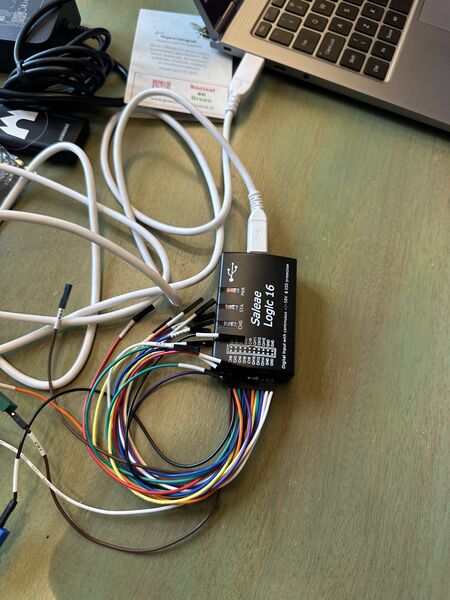
Logic Analyzer: Like an oscilloscope for digital signals. It allows you to see relation between multiple parallel signals. Henk shows a Chinese rip-off (4 euro) that works with the software from more expensive vendors (like Salea). Henk also mentions Pulseview
Designing
Design that Erwin made during his FabAcademy
The end result; no everything has to be a square
Yes and then there is Kicad. It has grown substantialy in the previous years regarding functionality. Procudure:
- first design in a logical way (Kicad schematic)
- then use that to create a physical design which you can print (Kicad PCB)
Erwin shows a design he made in the past; it was simple enough for him to directly connect the wires in his design He also shows another example using labesls "output on the MC" somewherer else also output. When you have a large design this is probably the way you want to desing; give more overview.
Note
Tip from Erwin are the videos from Shawn Hymel has a lot of Kicad tutorials. Remco acknowledges and adds "he also created FreeCad tutorials"
Ok, so why can we use Kicad so well, that's Kris has created a library for Kicad in which he has defined all components that are commonly used in FabAcademy. Why would you need that? Well to draw schematics you need to know symbols and footprints per component. (that makes sense )
BUT(!) Henk mentions: "schematic doesn't mean it is layout in the real world. For example ATtiny, the schematic shows all pins almost on the same side, but PCB editor will use the footprint definition were there are 4 pins on each side. Erwin later on mentioned that a MC can also have different form factors; so be aware.
Erwin: you start with the microprocessor in mind. Henk shows that Erwin has devided everything very nicely into areas / power, connectors, MC, ...
Then to sum up some remarks:
- Henk: "PCB editor that's were you spend the most time ..."
- Henk: "we (fablab Amsterdam) only use lanes at one side of the board; not two ("we are prototyping")" and refers to example of board, made in China, that didn't work; because a capacitor was to far away from the micro processor
- Kicad can also export a bill of materials
- Erwin: "PCB doesn't care about the value of a resistor that much; as it has little effect on the form factor
- Erwin: "PCB: purple line points out that nothing can be place within; these are physical boundaries(!) not electronic boundaries
- Henk: "we will be using the MDX20, has 0.4 mm frees bit"
- Erwin: shows that Kicad PCB helps to check connections and distances between components. You can ignore the warnings/ errors of course.
- Erwin: shows 3D viewer as well; looks very cool
- Erwin: FreeCad has Kicad plug-in (I wander is there one for Blender?). This is particularly handy to create a case after designing your board
- Henk refers to https://gerber2png.fablabkerala.in/. According to their website. From Kicad you export as PLOT and
gerberfiles (don't forget to select drill files) and drop them on the website
Gerber2Png is a JavaScript-based React application that runs directly in your browser. It allows users to load Gerber files from various EDA software (such as KiCad, Eagle, Fusion 360, Proteus, EasyEDA, Altium, etc.) and convert them into black-and-white PNG files. These PNG files include traces, drills, and board outlines, making them suitable for PCB milling operations in Mods. This tool simplifies the process of generating milling-ready images for both single-sided and double-sided PCBs. It is hosted at Gerber2PNG and built using modern JavaScript libraries with a React-based UI.
Group assignment
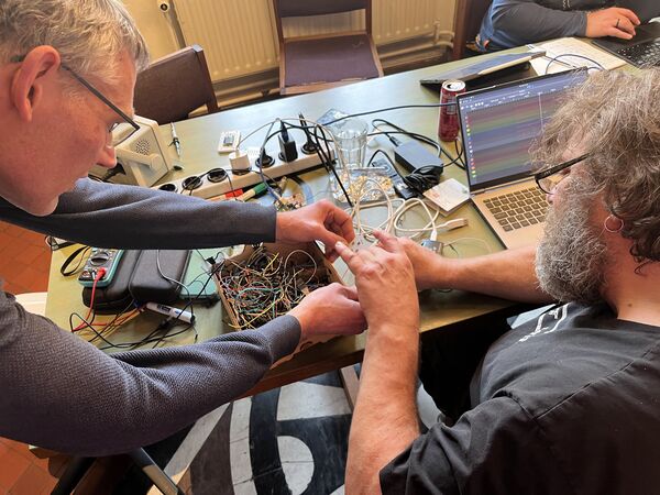
Erwin has created an eletronic puzzle for us. A mysterious Arduino UNO that does stuff ... but what? Our assignment, if we're willing to accept it, is to find out it's behaviour using the test equipment. What pin does anything and what is it doing?
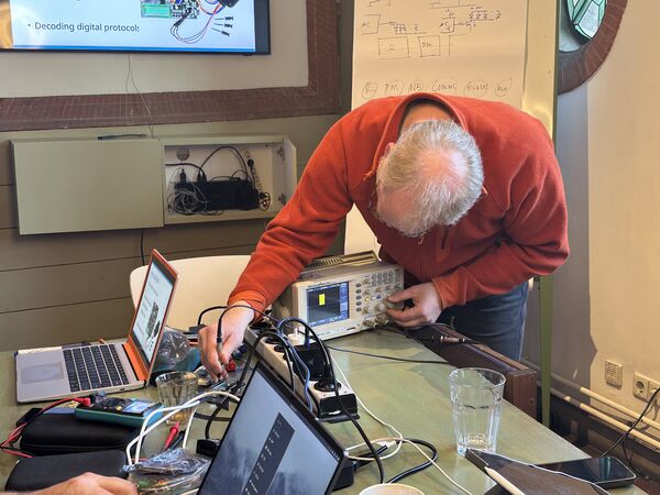
Anyway, we did not really use the multi-meter. The reason mainly being that we needed to analyze behaviour on the pins of the Arduino and no to much if there was a voltage to be found. For this reason we only used the oscilloscope and a logic analyzer.
Oscilloscope
What we did is to at least connect the base of the oscilloscope to the GND (ground) of the Arduino. Then we connected a pin (image below shows pin 7) to the channel of the oscilloscope.
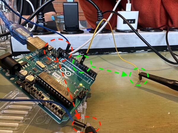
Remark: all pins 13, 12, 11, 10, 9 and 8 did not show any behavior
PIN 07
- output was 5V all the time
- probably default behavior, not programmed
PIN 06
- a signal that, when turned on, is always 5V but the duration increased during 4 seconds, then drops and starts over
- this is Pulse Width Modulation (PWM)
- When attached to a LED, the LED will increase in strength, drop to nothing and start over in 4 seconds
So we attached a small breadboard that Erwin gave us and voilá
Note
Frequencies around 50Hz or higher can not be detected by the human eye. So when the frequency is 1000Hz it will switch on/off a LED so fast we don't detect it, we just see it more off than on in the beginning, but we also then see it increase because it will be set on longer during thos 4 seconds
Note
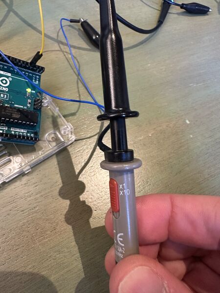
Another important thing is that the lead of the oscilloscope had a switch that had 2 options: "1X of 10X". We had it set to 10X which meant that signals would be scaled down 10 times. This explained why we detected 0.5V on a pin which is quiet unusual (as Arduino is either 0V, 3V3 or 5V). After setting it to 1X our measurement made more sense
PIN 05
Pin 5 showed a oscillation of 1000Hz whereby it was active 1/8 of the time. We expected to glow at 1/8 of its capacity (which was correct)
PIN 04
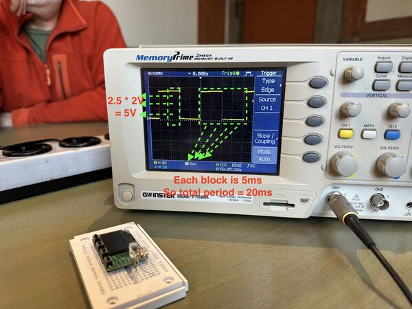
So period was around 20msec which gives a frequency of 1/20ms = 50Hz. This is again not visible by the human eye. As a human we will "see" this as a light that uses 50% of its capacity.
PIN 03
This was fun ... 1 second 5V and then 1 second 0V/nothing. So classic blink 1 second on and 1 second off.
PIN 02
We calculated a signal with a period of 666ms which gave us a frequency of 1.5Hz. The LED behaved like expected.
Note
Fun thing happened while we were testing Erwin's black box. The measurements we made after a while differed from the ones we made earlier. Erwin said that he did not programm anything special to misguide us. So after resetting the Arduino we got the same measurements; the Arduino basically was appearantly stuck in a loop or something. But why did the blinking go on? Why did the PWM still work.
That's because on the Arduino you basically "tell a piece of PWM hardware" to act as PWM. When the programm then has an error the hardware/ peripheral will still work/ do it's thing.
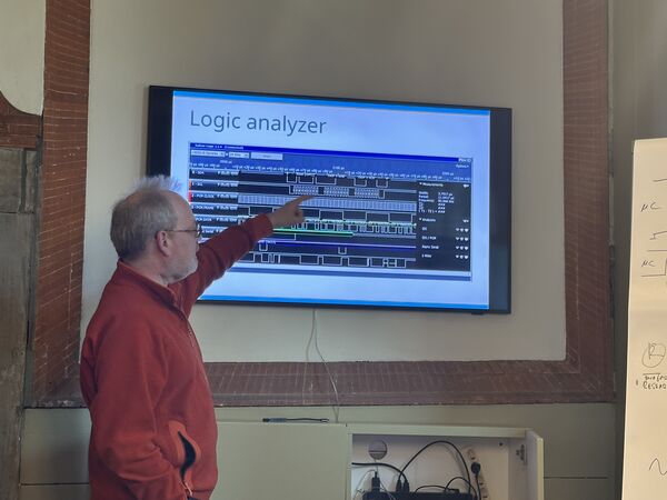
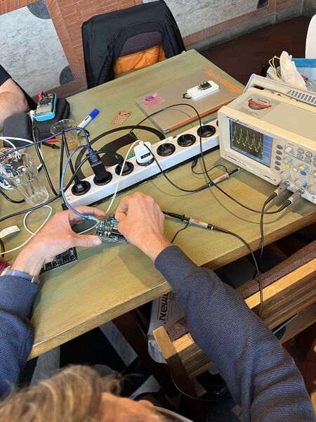
Logic Analyzer
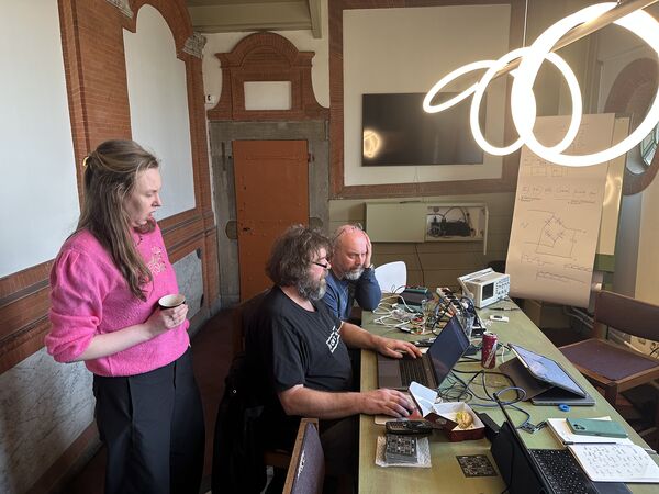
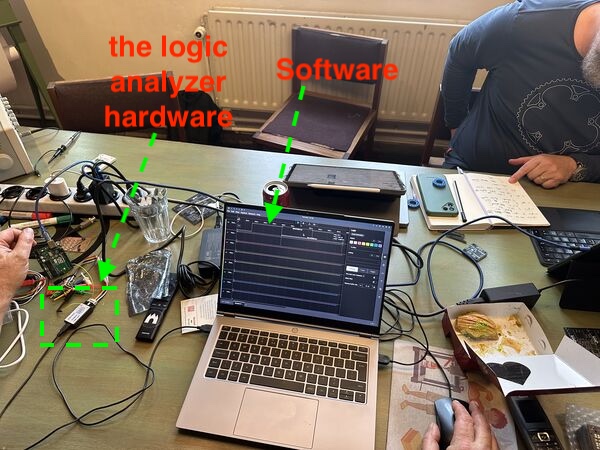
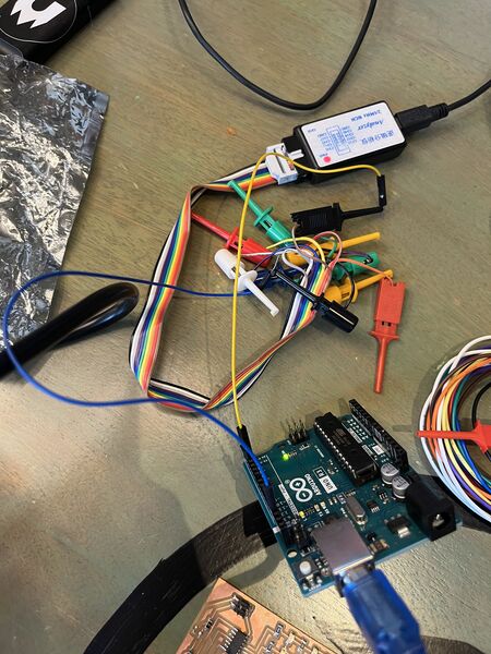
Henk showed us his very expensive logic analyzer (4 euro). The basic idea is that you can use this to analyse DIGITAL signals; even multiple at a time. So after connecting the base to the GND of the Arduino Henk connected 3 other pins: 6, 3 and 2.
Note
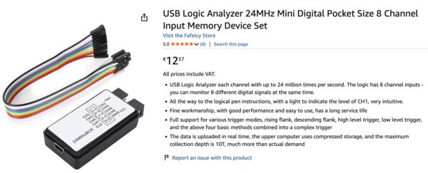
After math from Kris ... "How speedy is this thing" .. Well according to the description -> "USB Logic Analyzer each channel with up to 24 million times per second. The logic has 8 channel inputs - you can monitor 8 different digital signals at the same time."
As you can see in the video the channels 0 and 1 actually showed something. The top one
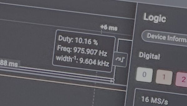
The software also gives you more detail than the oscilloscope. So for instance pin 05 .. According to us we estimates it's frequency to be 1000Hz and have a duty cycle of 1/8 of the time. The analyzer showed us 975Hz with a duty cycle of 12.9&.
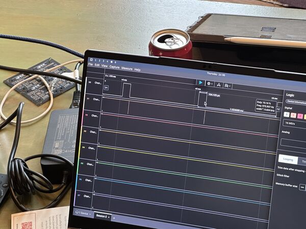
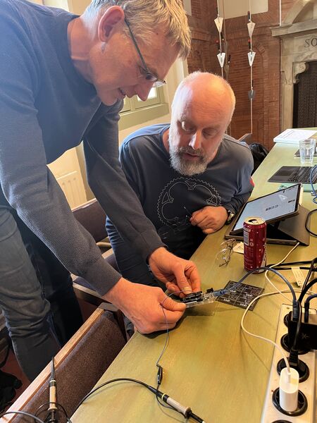
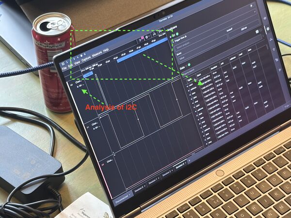
Finally Henk hooked up our QPAD from last week to scan the I2C port. He used different hardware this time.
Althoug we didn't take that much time for it, the software is able to no only show the signal but also "explain/ translate" this into commands. In this case commands meant for the display of the QPAD.
Invested time (approximately): 10 hours
Day 3 - [Friday - at the Waag]
Started around 09:45 ... updating documentation at home first ... Ended around 15:15 .. with documentation
Invested time around 5.5 hours
Day 4 - [Saturday]
Family day
Invested time: well a lot of thinking but not actually doing
Day 5 - [Sunday]
Started around 08:30.
Although I did no actual work on Saturday, I did think of possible ideas for this week and how to go around with the material we got on Wednesday.
Design ideas
G-force
When we were driving in the car, on Saturday, and, as the car is filled wity people, I'm usually a bit moree careful in thee corners, speeding and stuff; it's not very comfortable if everybody is hitting their head because you like to have fun behind the wheel. Anyway I thought of some kind of measurement device that would display G-forces in the car in 2 directions. Hopefully thee car will never hit the 3rd dimension
Light
Other idea I have is to rebuild a system I made at home.
It is triggered by one of two buttons, activates a 12V LED light outside the gate, and keeps activated while there's movement. After two minutes of no activity it will turn the light off again. If somebody comes by the movement will not trigger the light.
Boiler
At home we have a boiler from Nefit. It takes care of heating and warm water. To control the temperature in our house we use Tado. Tado has a switch on/off via a relais or OpenTherm protocol. However our boiler only understand relais language (on/off) and it's own propriatery EMS. A standard converter is not being sold anymore. Some people have designed an interface for it. So why not built it myself
In depth experiments ideas
Given the local class last Thursday I was also intriged by the logic analayzer regarding the i2C protocol. So maybe make a small programm that prints something on the screen of my QPAD and see if I can see that happen?
Oh and PWM (Pulse Width Modulation) ... make small programms to control my LED and see what happens using the logic analyzer.
Note
So yes I bought myself a logic analyzer.
But back to design spiral, my plan:
- go over the list of tools to design and/or simulate and pick 3 variants
- use these to design a simple thing and simulate it
- pick a tool that I think is going to be promising for me and do one of ideas
- design an idea
- dive into i2C a bit more
- dive into PWM a bit more
The world of EDA - Electronic Design Automation
As always to design anything I can use a piece of paper, pen and draw. And still as a start it's not bad. Neil also mentioned this during his class. Like using drafting tape.
Then, like I have done before, I would make a breadboard and experiment with stuff.
But my take of the class, is that there are many tools that can help me designing a schema in which I layout a number of electric components in such a way that it fits a certain (pre-defined) space, in such a way that the components do interfere with eachother (DRC (Design Rule check), ERC (Electrical Rule Check)).
So the class page lists a lot of possibilities and before diving into those I asked Google top 5 electronic design tools
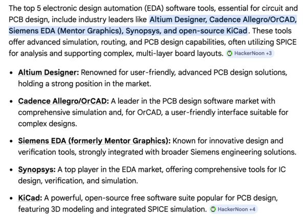
So Kicad and Altium are on the global class list as well. And of course I get tons of other links .. but then I thought to narrow my search a bit down: top 5 electronic design tools open source simulation.
This also gave me a link to a Youtube video about the top 10 simulation tools from 2025.
Note
The video mentions a number of tools of which Kicad makes no part(?) but it does help me to realize that (again) some software is very good in only analogue analysis like LTspace and TINA-TI. And can do both like Proteus; which looks very nice but is way too expensive.
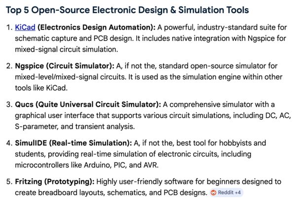
So my next search: top 5 electronic design tools open source free digital and analogue simulation DRC ERC. It gave some explanation about the features of the top 5 and a nice summary
Note
As a side step ... While searching I see all kinds of words that needs some explanation:
- SPICE: a general-purpose circuit simulation program for nonlinear dc, nonlinear transient, and linear ac analyses
- ngspice: ngspice is the open source spice simulator for electric and electronic circuits.
- ltspice: powerful, fast, and free SPICE simulator software, schematic capture and waveform viewer with enhancements and models for improving the simulation of analog circuits.
Ok so all about simulation.
So it's now 10:30 and I need to get started. My shortlist sofar (based on the outcome of the searches and cross referenced with the global class list):
- Fritzing: Highly user-friendly software for beginners designed to create breadboard layouts, schematics, and PCB designs.
- KiCad: mentioned by everyone; also because it includes native integration with Ngspice for mixed-signal circuit simulation.
- LibrePCB: full EDA workflow, including library management, schematics, and PCB editing, with built-in DRC & for beginners or those frustrated by the complex library systems of older, established EDA tools. That might be me
- Altium Circuit Maker (optional)
Project "Start"
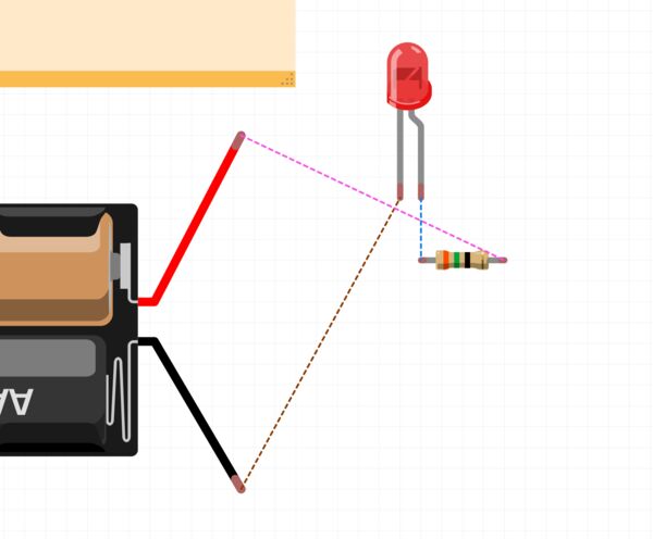
So for comparison I will make a design that's a mix of digital and analogue components use a micro controller (preferable the XiAO RP2040 from SeeedStudio), button and a LED that will blink after the button is pressed (1 second on/off).
The idea is to design, simulate the programm and end up with a PCD board.
Fritzing
Appearantly Fritzing is open source and I can access it via GitHub but getting the direct download requires euro 8,- which I'm happy to provide.
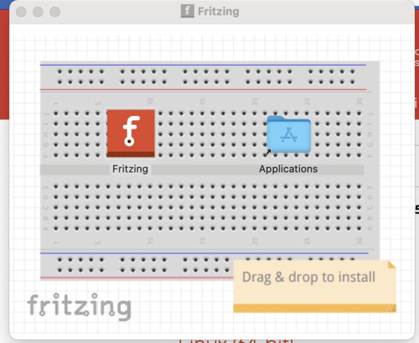
Just clicking around a bit on the parts it saw it will dynamically import part information based on the supplier you have chosen
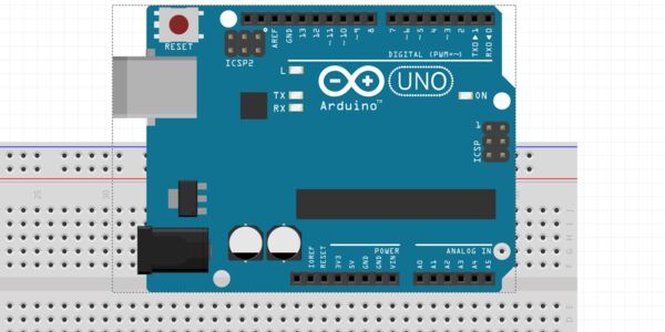
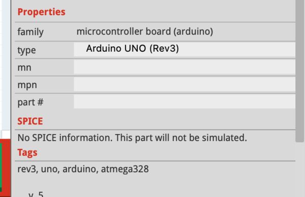
After starting a new sketch it showed me a breadboard after which I added a Arduino UNO to it (that is based on the ATMega328); similar to the one on Thursday. However I saw "this part will not be simulated" as there is no SPICE information; hmmm
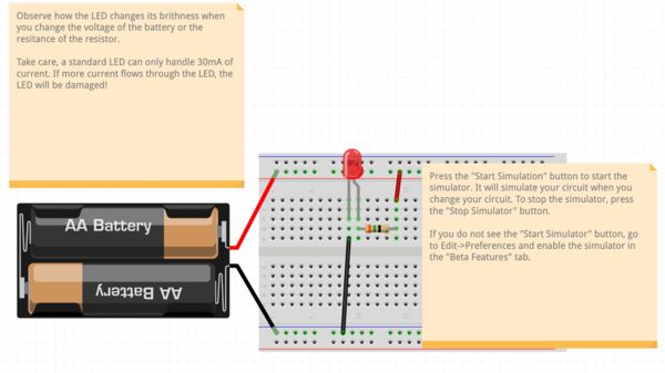
Fritzing does provide examples and I used the LED example (File - Open Example - Simulator - Basic Circuits - LED) to simulate a burning LED.
I then also clicked on the LED and resistor and saw some kind of SPICE information
Ok, what about I delete the resistor. Will it burn the LED (electrical rules)?
But then I could not remove the resistor ... really difficult .. I selected it, but after delete it removed the breadboard not my resistor.
I tried a bit more but gave up ... editing should not be that difficult; even if it is easy, this is not intuitive.
End of Fritzing for me.
TinkerCad
Ok TinkerCad was not on my list to begin with but I saw a collegue of mine use it before. Let's try that one to ad least create some kind of simulation with a breadboard. And appearantly I already created an account with them so logging in was fast. I didn't know that it is now owned(?) by Autodesk.
Note
TinkerCad also provides a way to create 3D designs; however tempting I will skip that for now.
I opened up a previous design and was back to a blinking LED using the Arduino UNO
Other features are that I can quickly click on schematic overview (to be exported as PDF but NOT editable) and 'bill of materials'
From a parts perspective it provides a limited set of microcontrollers like Arduino and microBit; for the full list
Let's try it
Ok what happens when I remove the resistor? Well nothing, no blinking. And if I connect the LED again? Well that's good, it shows there is something wrong
But no information on what is wrong afterwards; I can't find it.
To conclude, it is a nice program but because it has a limited set of parts (no possible to import the FabLab list). I used the share option to create a BRD file. See if I can import that somewhere else later on. For now TinkerCad is also off my list.
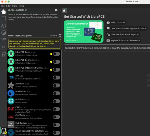
LibrePCB
LibrePCB promises a lot
LibrePCB is a free, cross-platform, easy-to-use electronic design automation suite to draw schematics and design printed circuit boards – for makers, students and professionals, from beginners to experts.
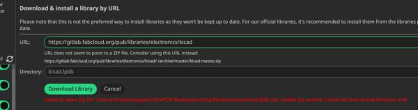
After downloading it won't start ... reading the installation instructions
Unfortunately we’re not able (yet) to officially sign the macOS binary. Therefore macOS refuses to start LibrePCB by default. As a workaround, you need to run it once with Right-click Open on the LibrePCB application in the Launchpad. If this doesn’t work, try it a second time.
Well that didn't work either so using the general security settings I found the app and could start it anyway.

After opening I used the default settings to set it up. Then, as there are no libraries yet, I used the library manager to import Arduino stuff.
From here I guess they have many more and I assume that standard LED's and resistors are part of it as well. Let's try. I created a new project and used the default settings again. It created a schematic section and a board section. Also 2 tabs main and default. The default tab warns me that I have to setup a schematic first and setup desing rules.
Setup schematics
I quickly followed a tutorial. My summary:
- Before starting with the board layout, add a schematic = boundary with some info
- Add
componentto either add: - a placeholder for a component (all you need in a schematic, but it does not represent a concrete part and does not specify the package to be placed on the board)
- a specific device (the combination of a component and a package with a particular pinout)
- a specific part (represents a real, orderable part; also defines the exact Manufacturer's Pat Number (MNP) which will appear in the Bill of Materials (BOM))
- Need more space to draw? Add more sheets; to connect them use supply symbols and net labels
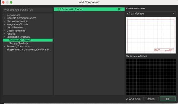
But using the add component option does give me the option to add a schematic.
The Add Component dialog lists all the components, devices and parts available in the libraries you have installed in your workspace. If you are missing something, you either need to install more libraries or create your own library elements.
Aha so that's why the library manager shows stars next to the LibrePCB labeled elements
Again used the Add component option, selected the right one and voilá ...
Simple LED
Well the drawing part is quite easy. Just add components until your done and then draw the wires. While I'm drawing Electrical Rule Checking takes place as you can see in image below; as I don't have attached the GND yet to the LED.
I didn't see the option to simulate; something with output jobs; so I decided to look that up.
At the end of every PCB project, we need to generate various production data files, e.g. for PCB manufacturing, PCB assembly, or simply for documentation purposes. LibrePCB provides a unified interface to generate any kind of production data for a project. It is called Output Jobs.
Ah so to continue somewhere else ... There are a number of job types like Gerber but nothing to do with simulation(?)
So where do I go from here if not simulation? Well the board itself. So I continue with my tutorial. And come to the conclusion that the Arduino has to power(!). Let's add that first ...
Ok so don't know what's the error here. I'll skip for now, maybe it becomes clearer later.
Note
What I expected is that the tool would give me more info about the error so that I either know "get rid of it or fix it"; now I don't yet.
Getting to the next part; the board
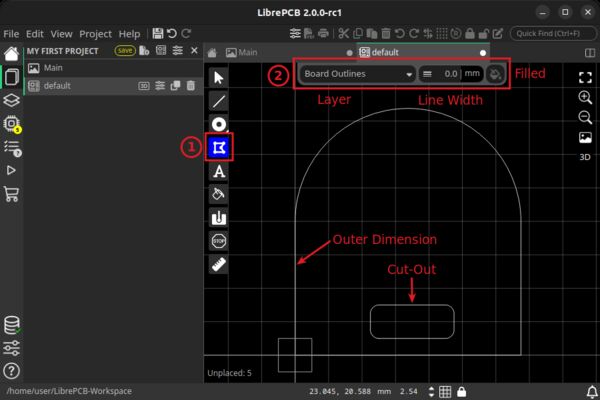
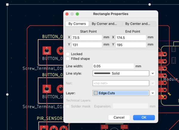
Once the schematic is (more or less) complete, you can start designing the PCB in the board editor. The most important thing of the board is its outline. Generally there must be a single, closed polygon on the Board Outlines layer. It is recommended to set its line width to 0.0mm since — in contrast to many other polygons — this polygon does not represent any actual material but only the outer dimension of the PCB. All polygons on the Board Outlines and Board Cutouts layers shall represent the actual board outlines (i.e. the edges), NOT the paths for the milling cutter! The PCB manufacturer will automatically offset the outline polygons to calculate the actual paths for the cutter.
After adding my border outline = polygon I added my components
So I fixed this and also removed the outer lining which was apperantly already a outer border
Once your design is complete, you should run the design rule check (DRC) to ensure there are no critical mistakes. The check will report missing connections, short circuits and many more possible issues.
So I used Project - Run Design Rule Check
Ok of course, I still have to draw the traces; aiks .... Once I have done that I get clearance errors ..all three of them are near the transistor.
After setting the width of the traces to 0.2mm and rerun the checks it was ok. Well it kept complaining about the border line not being connected but I tried a couple of times and I think it is fine; I can't see any gaps.
Finally a nice 3D representation
Oh and a final check on the FabLab libraries ... is it able to import those? Nope ..
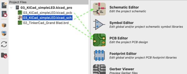
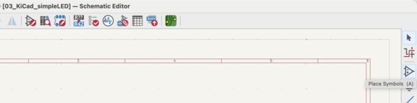
KiCad
As I already installed KiCad on Thursday but no used it. I choose for default settings to begin with and the user interface matcht the one I saw on Henk's laptop.
After creating a new project I saw that it created a SCH (schematic) file and a PCB file; like LibrePCB did. It also recognized the BRD file from TinkerCad as a PCB file(?). Opening the schematic file pressed me to initialize some kind of global library (recommended) which I did.
Then an intimidating user interface popped_up.
And when things get intimidating I have the need to go through a quick tutorial.
Before drawing anything in the schematic, set up the schematic sheet itself. Click File -> Page Settings Then add components
It was difficult to find the symbol that I needed and it looked quiet similar to another symbol. But I found the option after I recognized I was in the PCB editor; not the schematic editor. After switching I tried to add a Arduino UNO R3 (like with the other tools) and KiCad just crashed ... hmmm. Reopened it and soon had a basic schema at hand but the electrical rule checker was not happy.
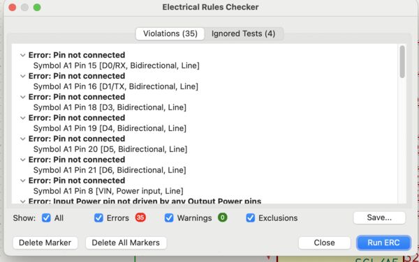
Well pins not connected I understand but is also not important. But what about the resistance value and the voltage for the LED and power?
Each symbol needs a unique reference designator assigned to it. This process is also known as annotation. By default, symbols are automatically annotated when they are added to the schematic. Next, fill in values for each component via the properties window Finally, assign a footprint to each component. This defines how each component will attach to the PCB. Some symbols come with footprints pre-assigned, but for many components there are multiple possible footprints, so the user needs to select the appropriate one (which I remembered from local class).
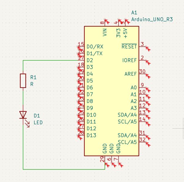
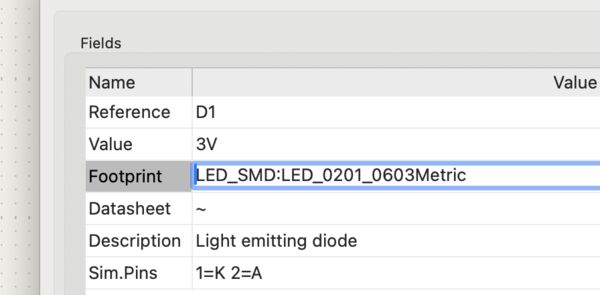
So I changed the LED to red and the resistor's value to 1k. Both of them I set to SMD type of components. Of course the Arduino already had a footprint. I used the associated datasheet to check that VIN pin is actually used for 5V in.
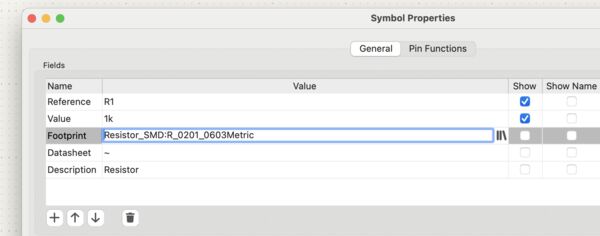
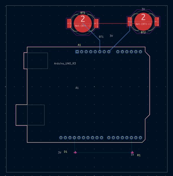
I changed the schematic a bit to clearly define 2 battery holders which I put in serie. I changed the values to 3V each.
Ending up with a board like this ..
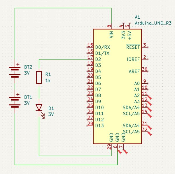
So when I run any kind of simulation / check it should tell me that 6V is more than the allowed 5V? Well the electrical rule check does not say anything. Simulation opened just briefly but I understand it for now. So let's first switch to the PCB editor.
First I setup the board using
File -> Page Settings(this is self explanatory)Next I used the option
File -> Board Setup… to define how the PCB will be manufactured. Here I tried to change the number of layers to 1 but the minimum number of physical layers is 2 (Henk told us that we would print on 1 layer on Thursday)
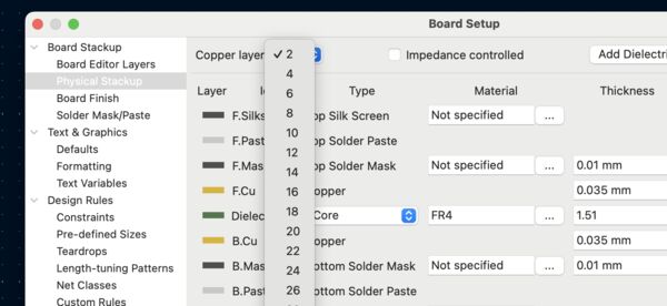
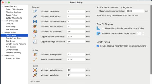
Next, I just looked at the default design rules using the option
Design Rules -> Constraints page. The settings on this page specify the overriding design rules for everything in the board design. I left it the way it was.
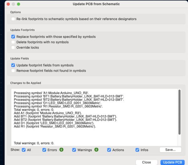
To import design data from the schematic into the layout I used
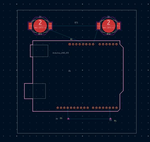
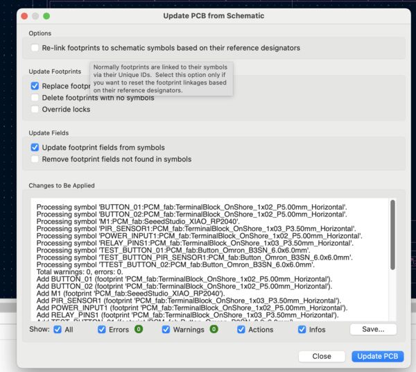
Tools -> Update PCB from Schematicwhich imported all the components from the schema. I placed them in the middle.
Then, like LibreCAD it is time to tell the tool where the board outline actually is. According to the manual
The board is defined by drawing a board outline on the Edge.Cuts layer. To draw on the
Edge.Cutslayer, click Edge.Cuts in the Layers tab of the Appearance panel at right. Etc... the only requirement is that the outline is a single closed shape that doesn’t intersect itself. Then I routed the tracks (like in LibreCAD). I had some difficulty with the batteries but I think I managed that
Design Rule Checking is the layout equivalent of Electrical Rule Checking for the schematic. DRC looks for design mistakes like mismatches between the schematic and layout, copper regions that have insufficient clearance or are shorted together, and tracks that do not connect to anything... To view the full list of design rules that are checked and to adjust their severity, go to
File -> Board Setup… -> Design Rules -> Violation Severity.
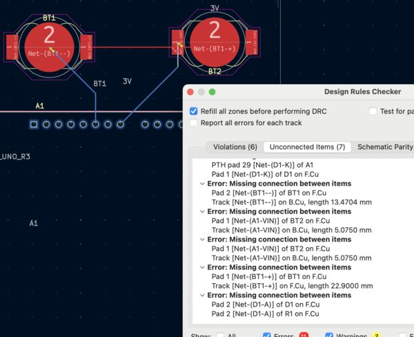
I run the DRC using option Inspect -> Design Rules Checker ... Well that made me happy ... :unhappy:
So after dinner I finished documentation for today and checked it in.
Invested hours: 9.5
Day 6 - [Monday]
Started around 08 this morning. My plan today is:
- fix the tracing of my latest
simple LEDdesign from yesterday in KiCad and get rid of errors - understand a bit more about how I can simulate with Kicad; does it support microcontroller simulation?
- Investigate integration between KiCad and FreeCad for casing; is there integration with Blender?
- re-design my
lightproject using only standard components; so no microcontroller and simulate it - (optional alternative) design a
blow out electrical candle - (optional alternative) design a
CO2 measurement device(that you can hang around your neck) - (optional) more PWM experiments using my own logic analyzer
- casing?
Inventory
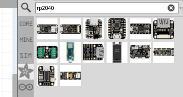
The individual assignment said something about using parts of the [inventory](https://inventory.fabcloud.io/). During global class Neil mentioned the work of Kris how created the definition of components and their foot prints for Kicad. So let's first take a look at those.
Why do this? Well I want to make sure that I use the standard materials/ sensors etc later on during the FabAcademy.
KiCad FabLib
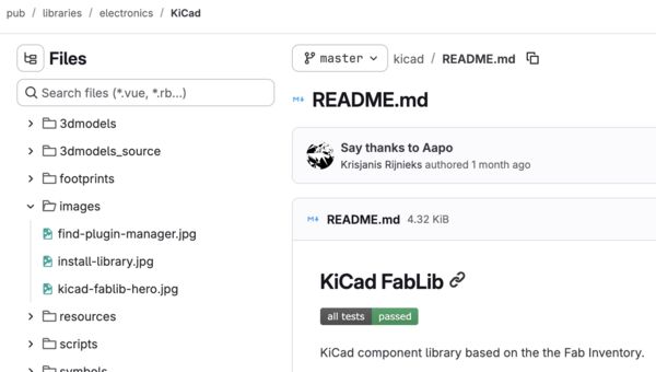
As it says in the intro KiCad component library based on the the Fab Inventory.
FabLib makes it easy to produce PCBs at a standard Fab Lab. There are more than 2k Fab Labs in the world and many of them will have electronics components from the official Fab Inventory. The goal of FabLib is to have 1:1 mapping with the parts from the Fab Inventory which reduces friction when learning electronics and boosts confidence when prototyping rapidly at a Fab Lab.
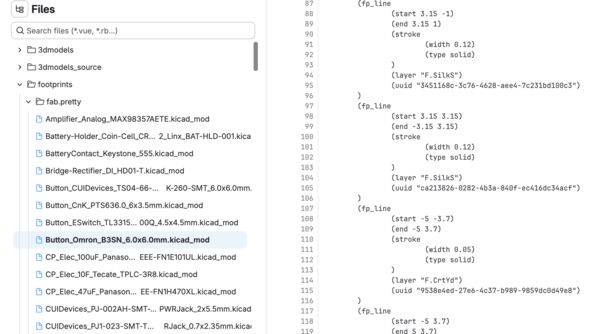
It contains installation instructions. Looking through the material I try to find images but my guess is that the shapes/ footprints are defined using descriptive language.
Anyway I followed the installation instructions.
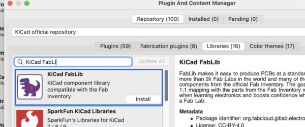
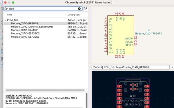
I tested it by trying to add the XIAO RP2040 from SeeedStudio ... and that was working nicely
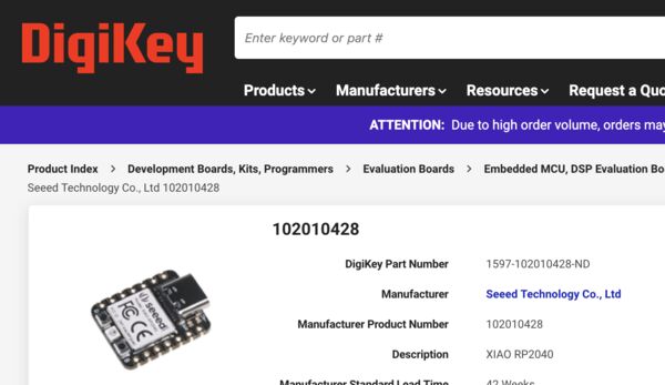
FabLab inventory
I used the link to take a look around. It is a comprehensive list of all sorts. Below I found the microcontroller we used and a link to DigiKey
Just to make sure I tried to find it in the KiCad library as well; and there it was
Finish my SimpleLed design in KiCad
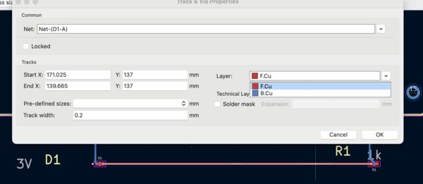
I trew away all my traces in the PCB editor just to start over; I did not change the schema. I did some simple tracing first by connecting the Arduino to the LED and from there go to the resistor. Then I found out that the resistor should be turned around. This was not very difficult (but why is it suddenly a RED line instead of BLUE?)
So let's look in 3D before I start connecting the batteries; just to make sure I get the idea of their form factor (and I draw the connections that I want to make later on)
Ok pretty much what I expected. Let's look at the LED and resistor I just traced. Why is there no line between the Arduino and the LED/resistor but there is one between the LED and resistor (which should be the case by the way)?
Ah that's why the line is RED ... it is traced on the back of the board; good to know . But I don't want that so .. Ah clicking on it I can easily change it's properties to BLUE.
Huh ... now all my lines are gone?
They are all on the back. LATFS (look at the f. screen) .. the RED color is actually the correct one as it means the "FRONT". Ok fixed. Now onto the batteries. Again what I want ..
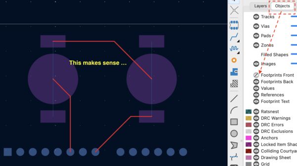
So I found out that you can filter what you see. I filtered out the Footprints front in the Objects pane. And saw that the lines I still had to trace were a bit messy. By turning around the batteries I could make it nicer.

Then by turning on the visibility of the Footprints front again...
Turning it off again ..
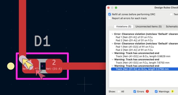
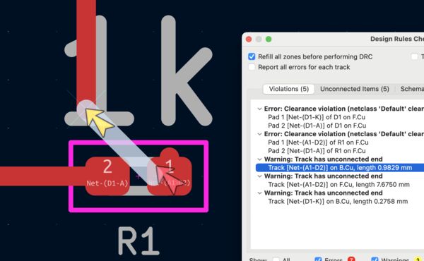
Design Rules Check (again)
I run the DRC checks again. The tool complained about a number of things among which were missing connections(?) near the LED and the resistor. Zooming in ...
So just added a piece of trace then tried to save it ...
Ah ... so I redraw the main line and voilá
Well yes and no ... No what's remaining are clearance errors
Then I remembered a link that we got from Neil during his class (or it was in the notes). Maybe there is something in there that will help me solve the clearance errors?
-[x] Number of layers set to 2 (already did that) -[x] Set Solder Mask Expansion to -[x] Design Rules Constrains (see image below). I increased any value that was lower than recommended. The others I did not touch.
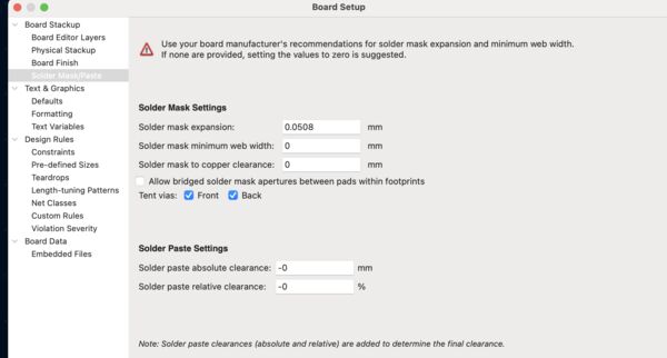
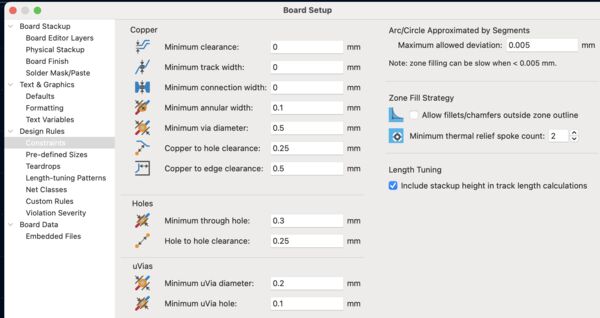
Note
The article mentioned other settings but I'm pretty sure we'll go into those during the production week~
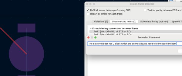
So I ran the check again and expected the same clearance errors of course because I just setup the rules to demand for more clearance... But before going into that I removed the errors about the missing connections with the battery holders. I added a comment.
Back to my clearance issues ... I rerun the DRC check and found that you can have a report about an issue
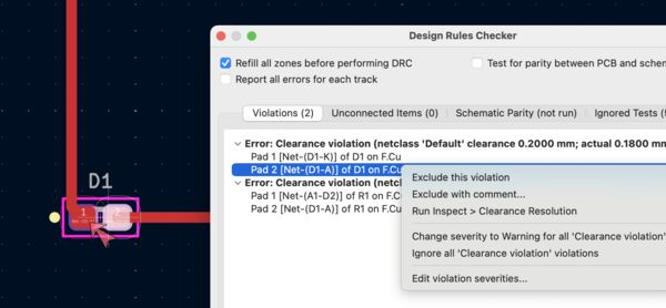
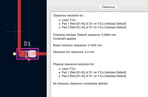
I asked Grok to explain to me what it actually means. Things I learned from this:
- I got this DRC error because the two pads of the diode footprint are physically closer than 0.20 mm to each other (edge-to-edge copper distance) and that's very common because the diode/LED is very small
- But because this LED/diode is defined to the same
net classfor all components it also triggers the minimum distance rule of 0.2mm. - Many small SMD footprints have pad-to-pad spacing in the ~0.15–0.18 mm range (sometimes even less)
So I went for option C which is to create a new netclass called "Tight" with Clearance = 0.15 mm and I assigned the nets of the LED and the resistor to this netclass. This keeps 0.20 mm for power traces / long routes, but allows tight spacing where needed.
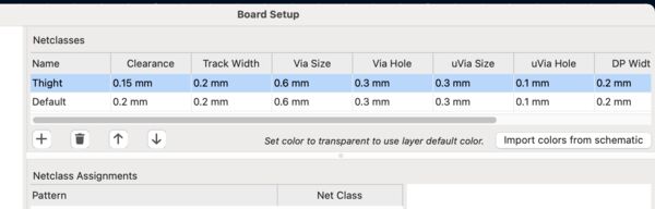
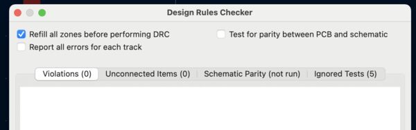
But somehow I did not find a way to assign the class to some of the components. For now I changed the overall default to 0.15mm. After rerunning DRC again there were no errors anymore.
Nets?
And to be sure what are nets?
A net is simply: A group of connection points (pins or pads) that must be electrically connected together In the schematic: Every time I connect pins with wires it creates a net. In the PCB, the net tells KiCad: "All these pads that belong to the same net must end up connected by copper (tracks, vias, zones/fills)". And ... the so called
ratsnest lines(those thin white/orange spider-web lines) are just visual reminders: "Connect these pads — they are part of the same net."
Ok vias? What's the difference between tracks, vias, zones/fills? Grok came back with an analogy (that I like):
Think of the copper on your PCB as a city road network: - Tracks = individual narrow roads for specific cars (signals) - Vias = tunnels / bridges that let cars jump between levels (layers) (ah so go the another side of a board) - Zones / fills = huge parking lots or express highways shared by many cars of the same type (usually GND or power)
Simulation in KiCad
It's now 12 and debugging my design took a bit longer than expected. But I still want to dive into simulation with KiCad. And hopefully I can simulate the Arduino UNO as well. I mean if TinkerCad can do it ...
I went back to the schematic editor and choose Inspect - Simulation which opened up a new window that was quite empty. So whenever I'm stuck (or I think I don't know what to do) I try to wacth a video first. I found a Youtube video from a year ago. And I basically followed the steps as much as possible. Well until 5 minutes...
What I learned:
- Select a component by searching voor SPICE gave me a voltage regulator and ground
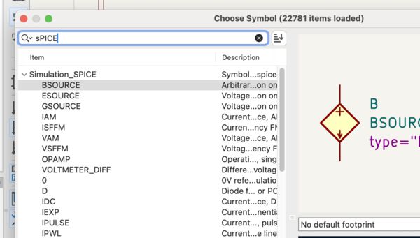
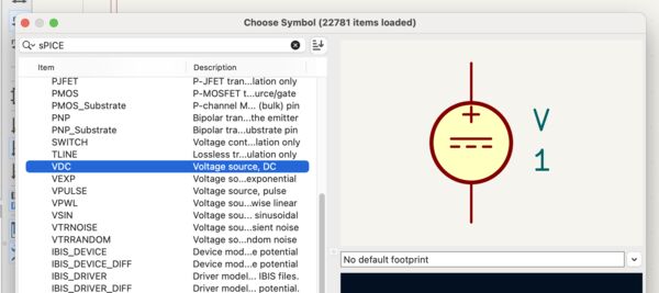
- Resistor (like one I used before) was a normal component
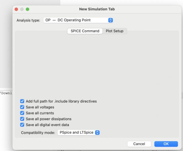
- Run the simulation by first selecting a type of simulation
- Back in the schematic editor I can still see the results of the simulation
Then I continued whatching and quickly found that it is not easy but it has lot of possibilities. Just watching I learned:
- I can exclude part of a circuit from the simulation
- I can delete a voltage supply and simulate it
- Select properties on any component and set everything in
Simulation model - If there is no simulation model I can choose the built-in one
- Or I can look for a SPICE model on the internet.
Note
SPICE stands for “Simulation Program with Integrated Circuit Emphasis”. This is a circuit simulator to simulate the electrical behavior of a circuit on a computer. With SPICE, electrical behavior including a basic DC analysis, AC (transient) analysis, and noise analysis can be simulated by creating a circuit model through a text command or a Graphical User Interface (GUI). SPICE was originally developed at the University of California Berkeley (UCB).
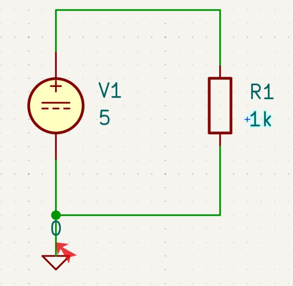
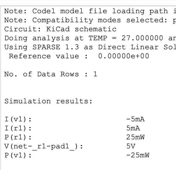
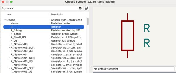
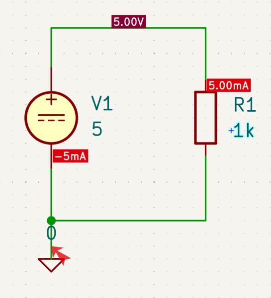
I decided to create a small circuit myself. I set the resistor to 1k Ohm and the DC voltage to 5V, gave labels to input and output of the resistor and try to run a simulation.
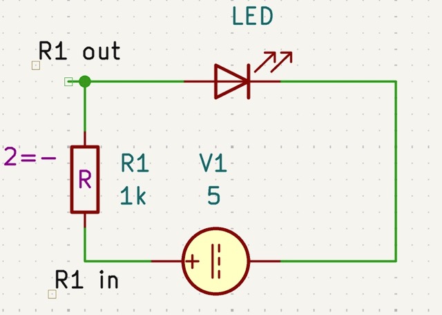
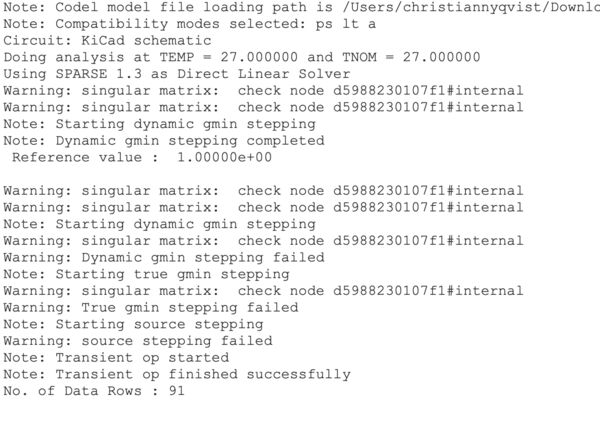
But something happened but also some errors. Plotting data showed nothing.
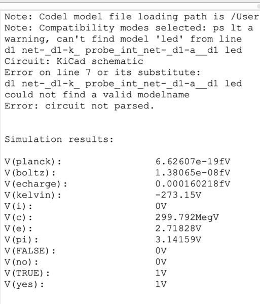
Going back to the schematic editor I checked that each component for a simulation model ...
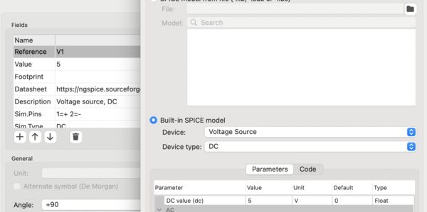
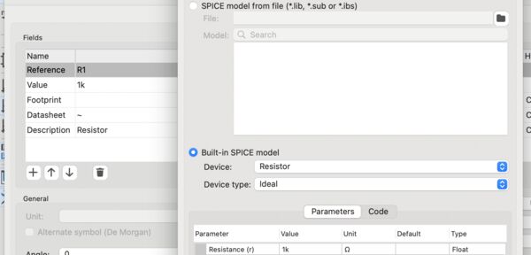
So the supply and resistor had an internal SPICE model attached them and the LED?
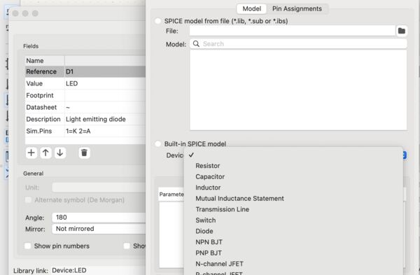
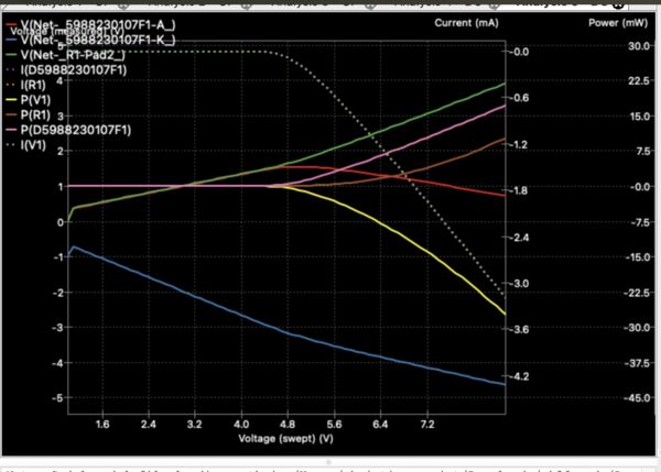
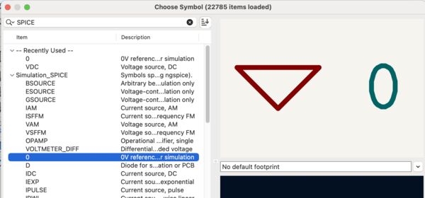
Nope .. So a LED is pretty common right? Searching for it gave me a lot of options. And there was no standard SPICE LED component that I could find in KiCad. What about the standard list from FabLab. There must be some LED's in there with specifications right?
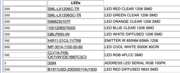
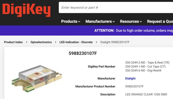
So from this list I choose 5988230107F ... but on the internet I could not find any standard model; also not within DigiKey. I did find a link to a PDF that describes how to make your own SPICE model for a LED.
That gave me the idea of asking GROK to create one for me based on the datasheet of this LED. Grok answered and did a nice job as well ...
SPICE doesn't model light output directly, but we can create a diode-based model that captures the nonlinear forward conduction, series resistance, and reverse breakdown—perfect for simulating current limiting, dimming, or array behavior.
.model Generic_Orange_LED D (IS=93.1p RS=42m N=4.61 BV=4 IBV=10u CJO=2.97p VJ=0.75 M=0.333 TT=4.32u)
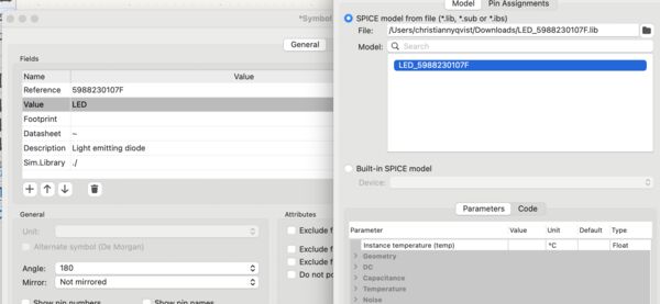
I saved this as .lib file and uploaded it as SPICE model with the LED.
The simulation ran and gave no errors BUT didn't gave me any plots? Looking quickly at the video I found that I had to select a different type of analysis: a sort of SWEEP analysis; in this case DC of course as that's our power supply characteristic.
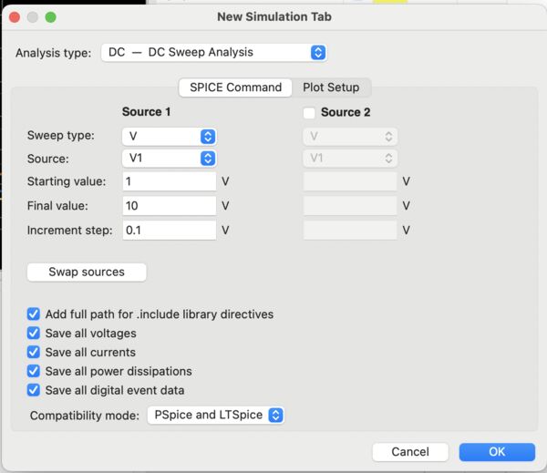
After running the simulation it apperantly ended but it gives some nice plots
So what about simulating micro controllers with KiCad ... well the internet is not very happy about that. It basically says no and that I have to export my circuit and use other tools. For now I leave the subject alone.
Redesign of 'Light' project
Just checking the assignment and FAQ it actually said ...
What does 'interact and communicate with an embedded microcontroller' mean? Answer: It means you must design a development board with embedded microcontroller. The development board must have local input &/or output to interact with the embedded microcontroller and enable microcontroller to communicate with external device(s).
Ah so my idea of re-designing my idea with just standard component without micro controller is not going to fly (is that even English?).
Current working solution
I build this solution not long ago. My daugther wanted more light in the morning when she went out or came back during the evening. Based on "movement detectors" I knew that just using that idea did not work, or would at least always put the light on, because we live near a road where there are cars, people, cyclists etc..
So the way it works is that somebody activates the light by pressing a button on the outside.
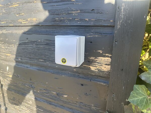
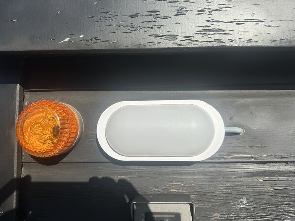
While there is movement the light stays on.
After 2 minutes of no movement, the light is switched off again. After that the light must be manually activated again; moving in front of the sensor does not activate the light.
Technical design
Because I had some experience with AdaFruit and Arduino I decided to build this whole thing using standard components; almost the official way. That lead to the following casing
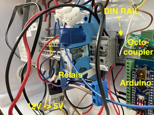
To power the whole thing I use a transformer to go from 230V to 12V (the heat sensor needs 12V) and I use another transformer to go from 12V to 5V for the microcontroller (Arduino Nano)
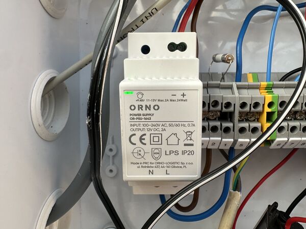
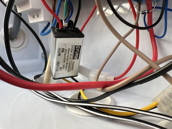
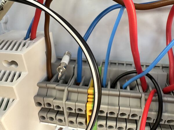
I used a fuse to protect the 230V - 12V circuit and to keep things tidy I use DIN-rail, and an octo-coupler to seperate the 12V circuit from the 5V circuit.
Lastly ...
For all technical details please see
Redesigning in KiCad
Ok I want to use the standard FabLab components as much as possible. So beforehand I will replace some of my components. For all comparisons I have used the official inventory list
Relay
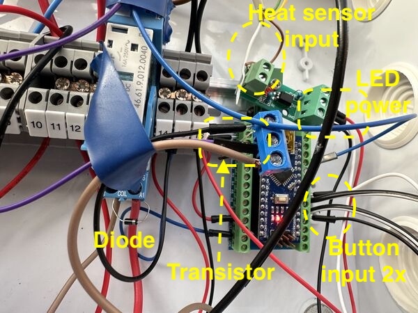
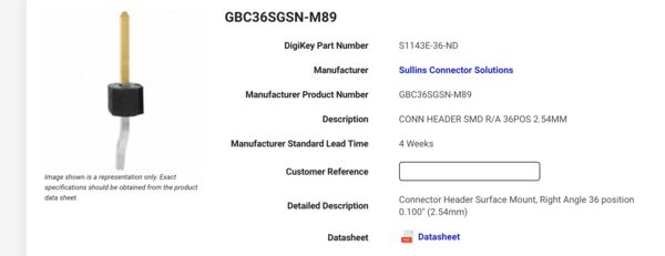
Currently I used a Finder relay to switch the outside lamp (230V; max 16A). Looking in the inventory list I found only one option, the CG Solid State Relay SSR-25DA DC to AC Input 3-32VDC To Output 24-480VAC 25A type B08GPJ1V2J. According to the specs it will be able to switch 48-480AC voltage based on an input range of 3-32V; perfect. But it's not in the KiCad list of components :sad:
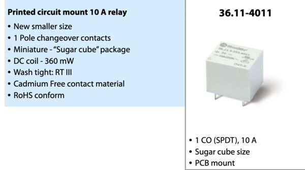
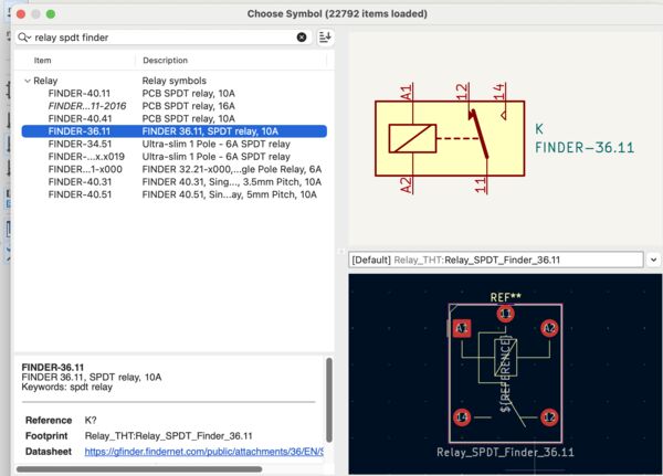
So I went for a Finder model instead. The 46.61 was not there. But it was meant to switch 230V/16A. As my outside LED light uses way less than 230x16W ... I picked the Finder 36.11.
Diode
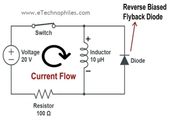
Erwin also told us on Thursday that, with a relay, you might want to add a diode that will prevent current flowing the other way around when the coil is switched off. This is called a flyback diode.
When an inductive load (e.g., relay, solenoid, motor) is switched off, its magnetic field collapses, creating a high-voltage, reverse-polarity spike. The diode provides a safe, recirculating path for this energy. It is connected in parallel with the inductor, but in reverse bias to the power supply (cathode to positive, anode to negative). During normal operation, it stays off. When the power is cut, it becomes forward-biased, allowing the current to "freewheel" through it until the energy dissipates.
I found two nice pictures explaining this visually.
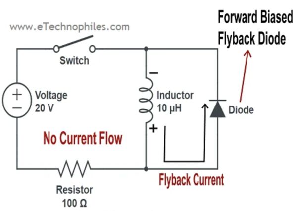
My current diode is a 1N4007 but as you saw in the images this is a through-hole not SMD.
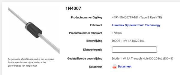
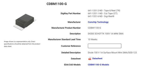
So I'm not able to explain why I need a diode that can handle 1kV/1A but let's just try to find one similar from the inventory. But the best I can find is CDBM1100-G and I think 100V is enough as it is switched by 12V. And yes it is part of the standard FabLab list in Kicad
It's now 18 ... for me end of day ..
Invested time: around 8.5 hours
Day 7 - [Tuesday]
Started around 09. I thought of some requirements that I need to explain to myself before continuing.
- I'm redesigning but that doesn't mean I going to replace everything 1-on-1
- While redesigning try to understand a bit better how the current solution works
- Try to think of a better solution; for example do I still need the octocoupler?
- What can't be changed is:
- main power source is 230V/16A
- LED lamp outside using 230V (I think no more than 6A; I lost the package)
- XIAO RP2040 as microcontroller
- Use of current outside buttons; no link to 230V!
Redesigning schema in KiCad (part 2)
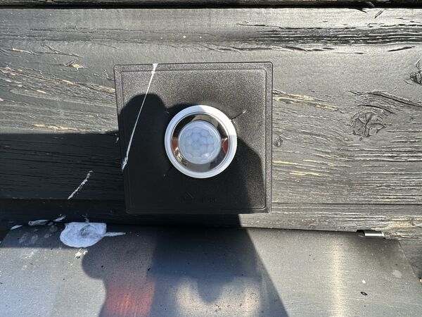
PIR
Ok, regarding my PIR26 sensor ... The one that I currently use ..
This is the reason (it runs on 12V) why I have an extra conversion from 230V to 12V and a relay that switches the outside LED lamp based on 12V. If I can get rid of the 12V altogether that save space, components I guess.
At the moment I can't find any alternative in the inventory list.
Talking to Henk I came to the conclusion that I'm looking at this week's assignment in the wrong way. Well not entirely wrong but I don't have yet to choose all input sensors. The idea is to create a board that I can play around with. But of course I need to keep in mind that I have to attach everything to it.
So he helped me get more focus. Also showed an alternative for my PIR sensor and/or relay. Also suggested to use a USB power supply on the outside and just make sure I get 5V to the microcontroller. So back to the drawing table first.
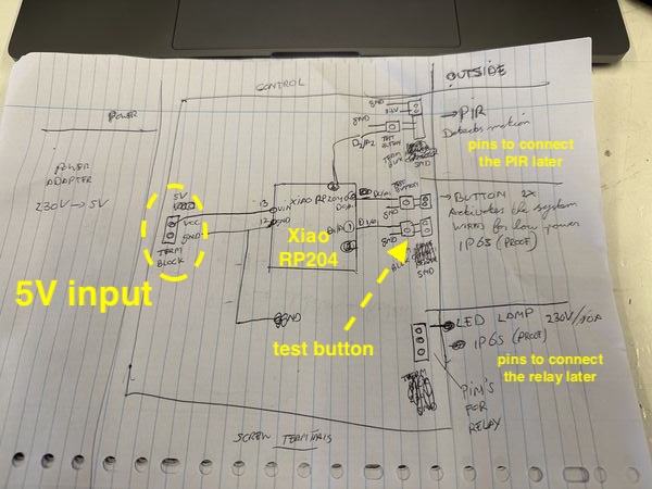
So with that in mind I just started drawing on paper first before use the schematic editor in KiCad. To refer to the pins on the XIAO RP2040 I used another website.
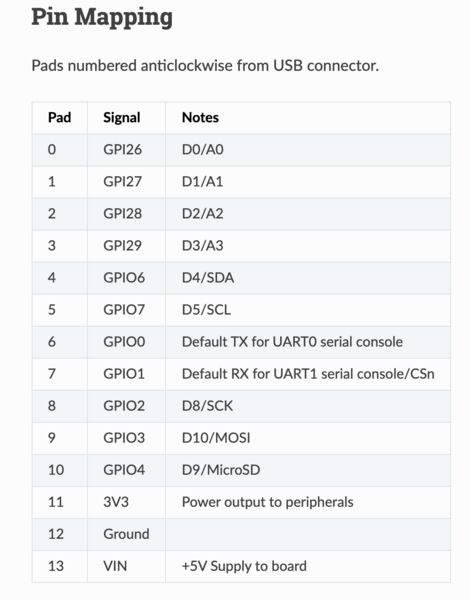
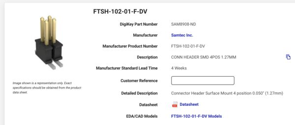
Also looked up two type of connectors that are from the inventory list and that I like to use later on

Temporary result ...
Redesigning schema in KiCad (part 2)
Ok after a while I got to this point
PIR sensor
As I understood from Henk it's possible to have a PIR sensor that works with 5V. So he gave me an example of one we have in our FabLab.
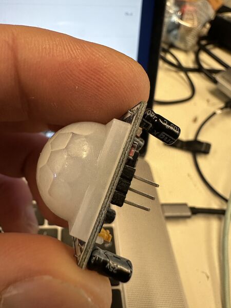
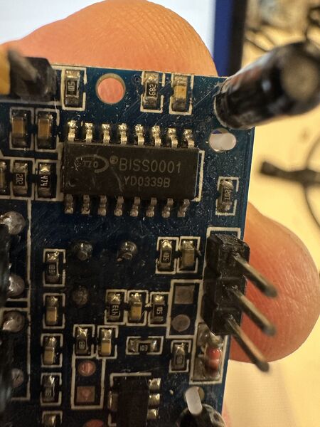
Based on the info BISS0001 I found a similar device on AliExpres.
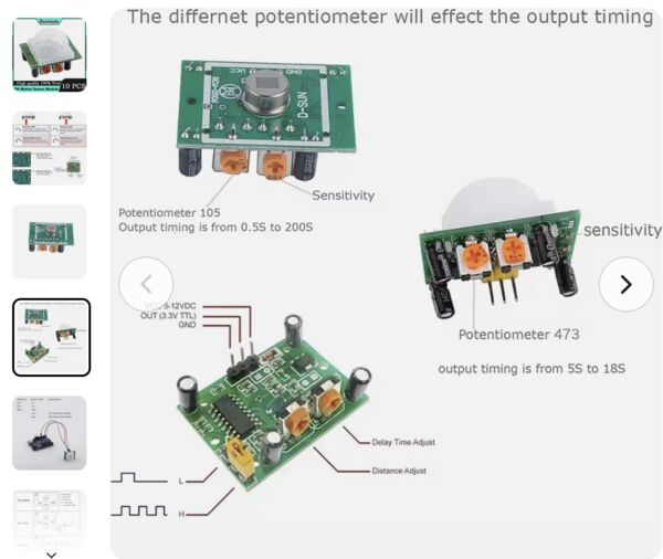
So what it tells me is that I need to connect the three pins to GND, 5V+ and to a pin on the microcontroller. And as the PIR sensor will be placed away from the board, it will be connected with wire to the board and I can therefore keep the screw terminals.
Relay
Regarding the relay, same idea. This one is able to switch 230V based on the output 3.3 of the Xiao RP2040.
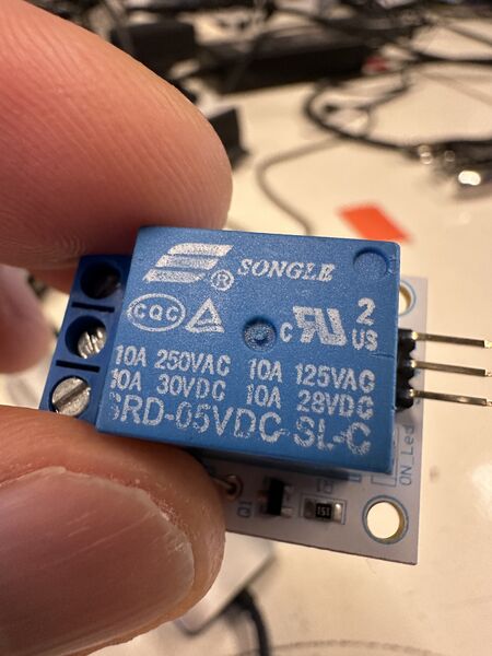
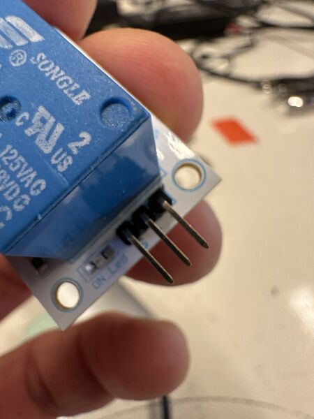
Well I didn't find it on DigiKey but somewhere with AliExpress again I found something similar.

From the image I can deduct that the three pins need to be connected to GND, 5V+ and to a pin on the microcontroller. And although the relay is near the board it will probably not be placed on top of the board according to Henk. So again I can leave the screw terminals in place for now.
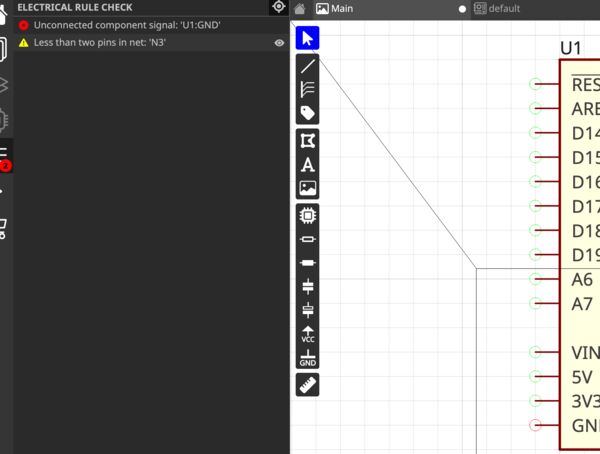
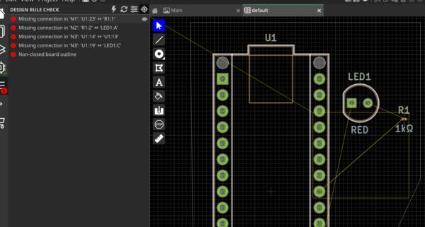
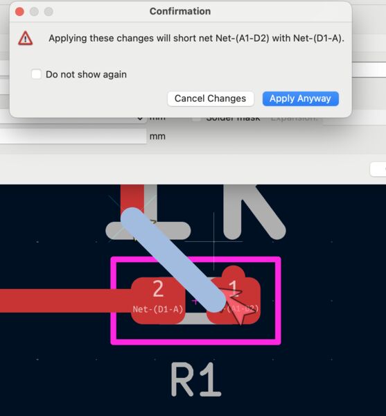
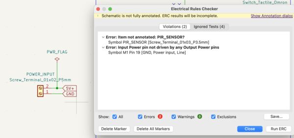
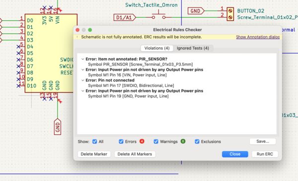
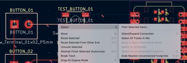
Ok let's check it by Kicad via the ERC (Electrical Rule Checker) ... Well not happy appearantly
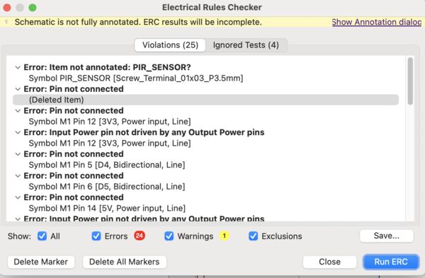
I excluded the violations were pins were not connected because, well I don't need them now.
Then it took me a long time to find error about a vertical line?? Ah.. there you are ...
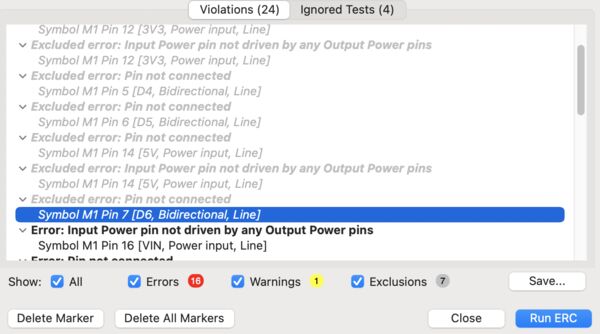
I rerun the ERC for now and, removing my exclusions, I was left with this.
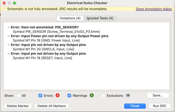
Special errors
So what does the error input power pin not driven by any Output Power pins mean?. This one I looked up on internet. It refers to an interesting video.
I learned that I have to flag any connection that is not used via a special marker tool. Aha .. As a result I marked them and rerun the ERC (after I deleted all my comments).
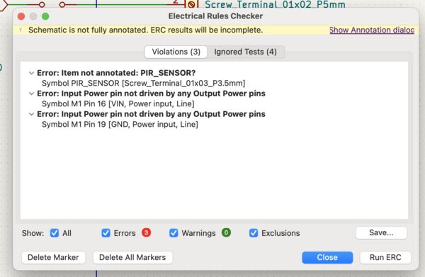
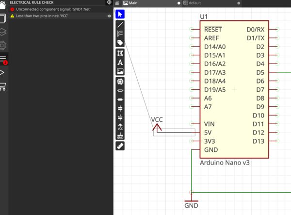
So I got 3 errors left ... So the error means that Kicad doesn't know which net carries the power. The answer is to add a POWER_FLAG to the input voltage. It's a component with a special name. So I did
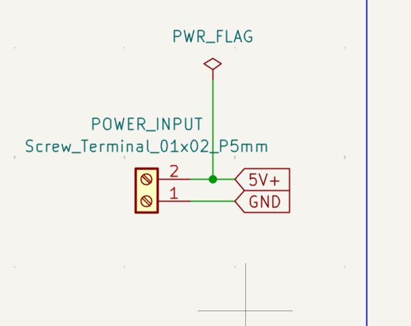
I rerun the ERCbut still a remaining error about power; this time linked to the GND?
Then I thought well probably have to do this for GND as well and I saw a POWER_GND component ... but ERC was not happy with that.
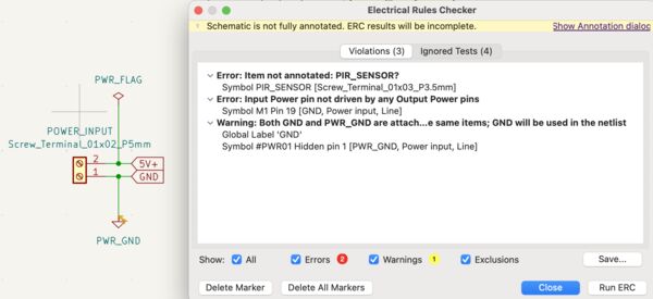
Hmm .. back to the video .. where I paused it and saw that this person also connected a POWER_FLAG to the GND. Maybe that's ok then?
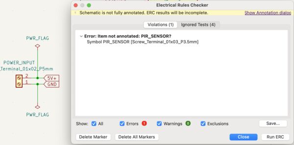
Yes! I'm getting there. According to the internet
Annotation, it’s the standard term for giving symbols unique identifiers in the circuit. Not invented by KiCAD, has been used in the industry forever.
I was not sure what to do but clicking on the error showed me the option to open the annotation editor. As it had selected the component I just choose Annotate which added annotations for that component.
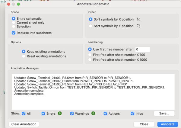
After running ERC again there are no more errors.
Designing PCB
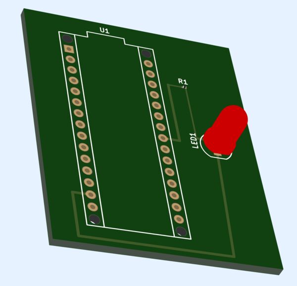
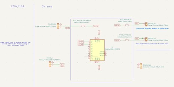
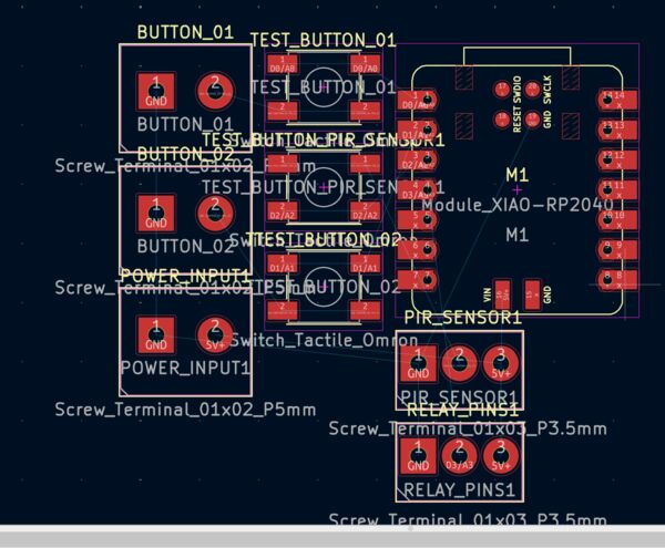
So time for my PCB. After starting the editor I imported all components first. This lead to no errors and a nice mess.
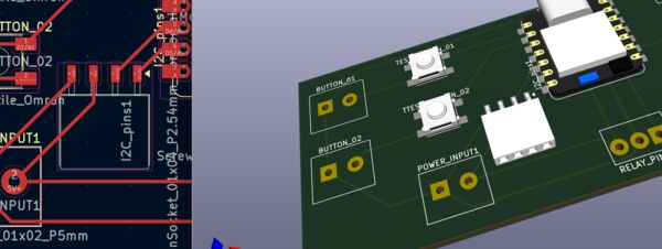
Looking at it from 3D point of view I would say it's perfect
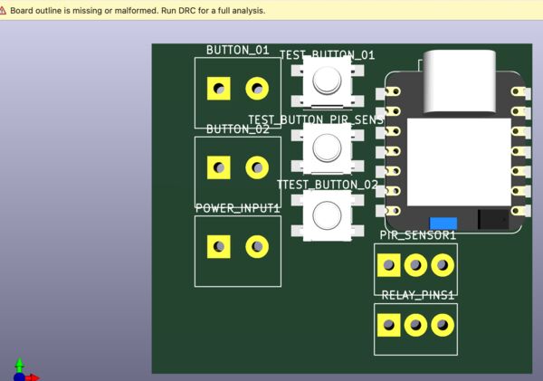
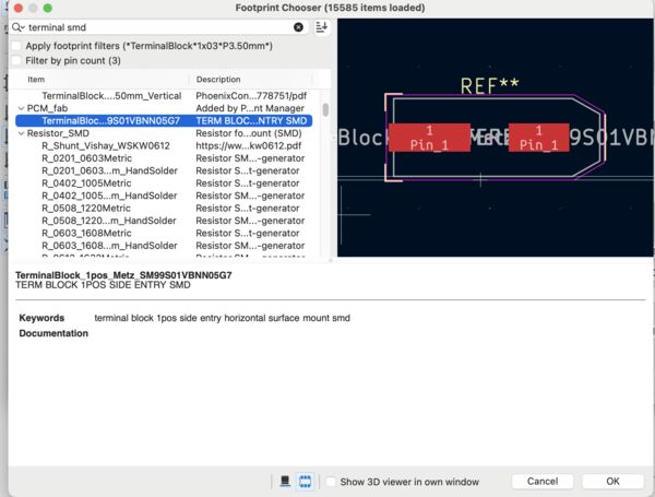
Ok the 3D view did point out that at the moment all the screw terminal blocks are through-holes NOT SMD. I tried to fix this in the schematic editor but I didn't quite figured it out yet. So my plan for now is to first finish this board and then, when there's time, update the footprint.
Ok back to the PCB .. after moving stuff a little I found the PIR connection a bit off ... Looking at 3D I saw that I actually managed to change the footprint.
Ok ... but let's make it through holes everywhere.
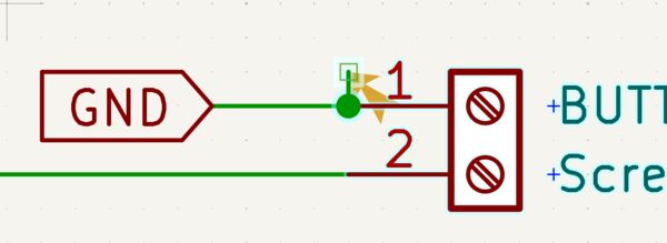
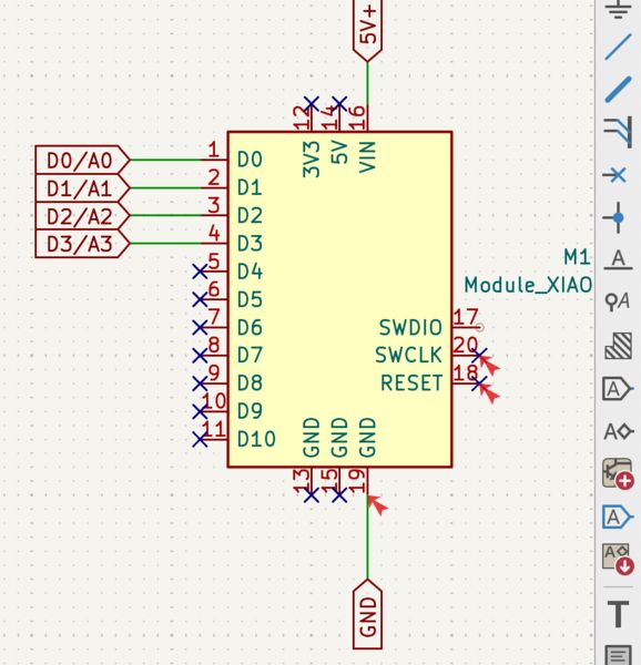
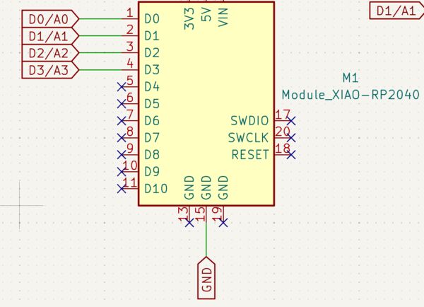
After this I started to draw GND and quickly discovered I choose the wrong GND on the Xiao RP2040
So I went back to the schematic editor, moved the GND, checked ERC and then updated the PCB again. This is fine for now.
I went on and thought "well this is not perfect but it will be ok" ... nope
Well at least I forgot to draw the edge and that was an easy fix
I then started over again after changing some labels in the Schematic editor ...
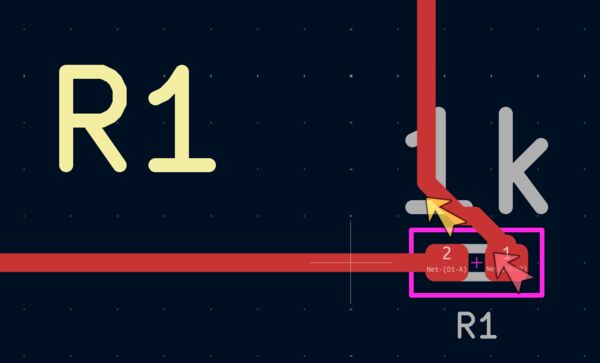
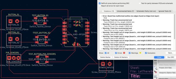
Finally I was done, I thought ... Well except for that one tiny error about a missing connection .. which made it impossible to finish (arghhhhh)
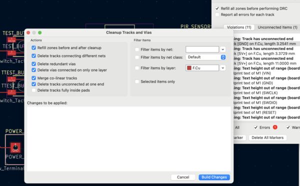
So I continued back and forth ... changing the schematics, checking it (ERC) and then updating the PCB. One tool that was very helpfull was to remove wires that were not closed. Because after you draw traces and you move a component ... well you can do it again
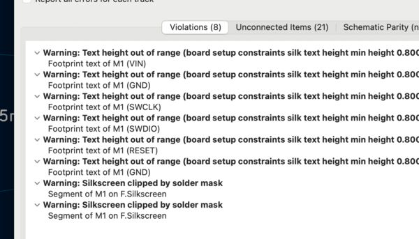
But yes finally, there it is ... except for a few warnings about the height(?) of text ...
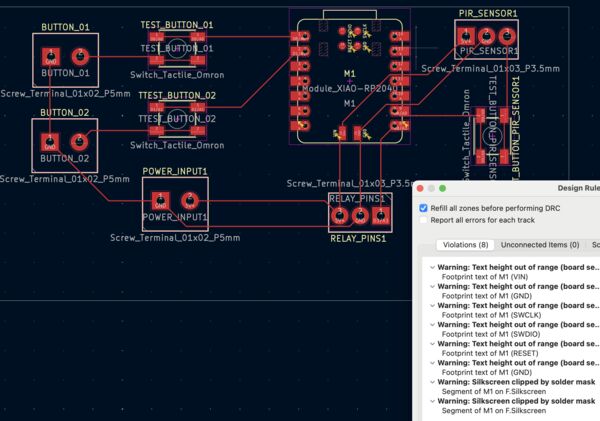
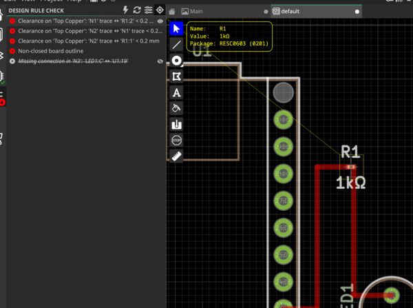
Finetuning my PCB
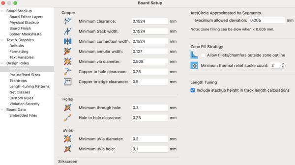
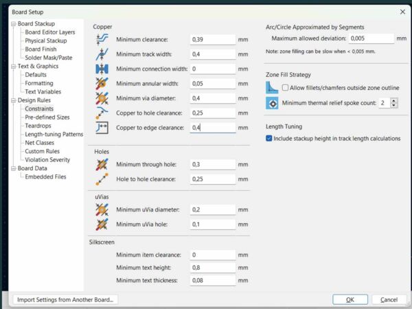
Irja and I had a small discussion about her design week. She referred to the design rules within the FabLab. So I thought it would be a good idea to include those as well. They are different values from the ones that Neil shared.
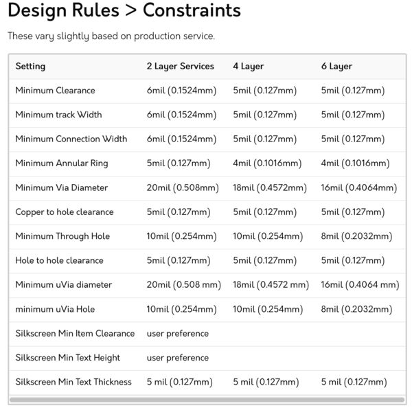
Neil's rules
Irja's rules
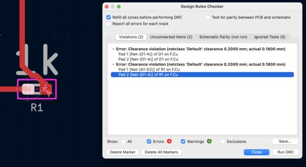
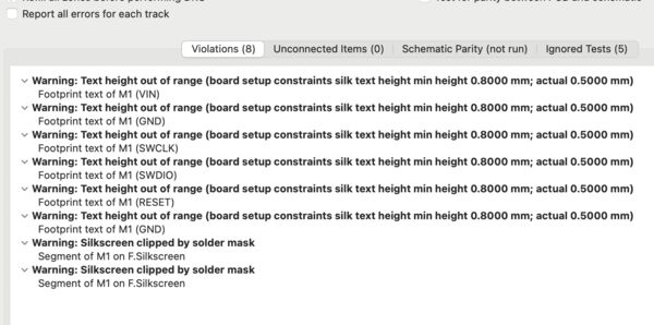
So I took the thoughest variant ... And ended up with a lot more errors
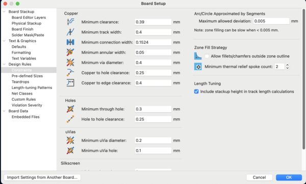
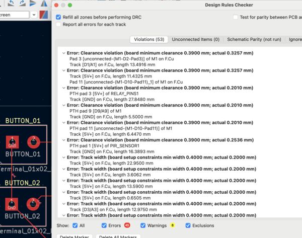
Well a lot of the errors were about the track width .. They are now 0.2mm and should me 0.4mm .. But there must be a way to change the width of the F.CU layer right?
But I first went back to Irja's documentation and continued about reading about her definition of Net classes and Physical stackup. Well I will do that anyway to see how much more errors I can produce
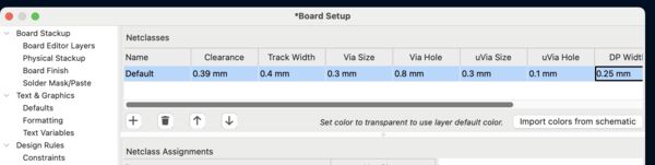
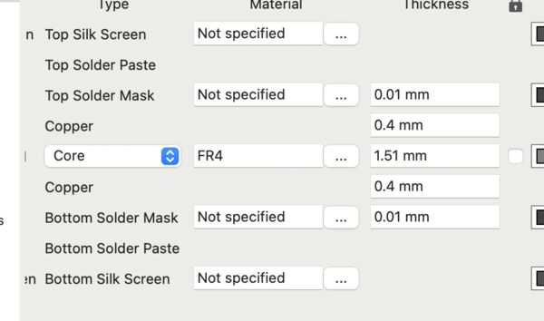
So again using File - Board setup I changed the values for netclasses and Physical stackup
I rerun the DRC again and yes a lot of errors; not more but quite the same. Irja wrote in her week that she basically traced everything using the wrong settings ... looking at the amount of arrows pointing to my traces I think I will also do that.
So I used the option Select ... and removed everything. After running DRC again I think I'm on the right track as the erros are again limited to warnings and I just have missing connections.
Well after redrawing the traces it was actually back to the warnings only.
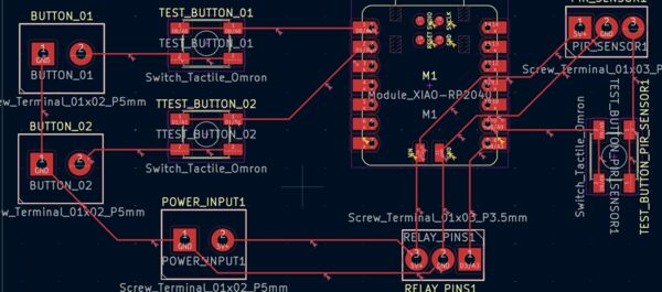
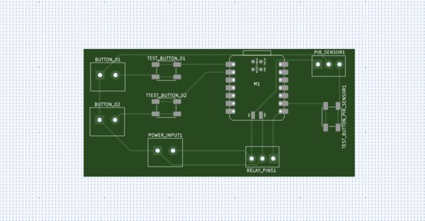
I ended with this
Time to make sure documentation is ok for tomorrow. And after I cleaned it up a bit I thought about gerber. I mean if I export it from Kicad and upload to this website and it understands it
I used the option File - Fabrication outputs and selected the gerber option.
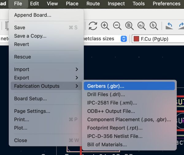
I got some screens that I used to Plot (and generated the drill files) and
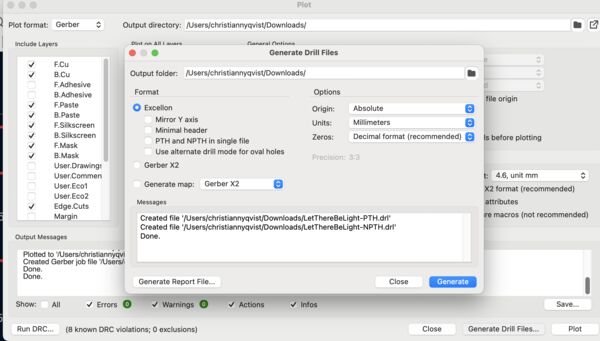
I imported this on the website and it was accepted without a problem
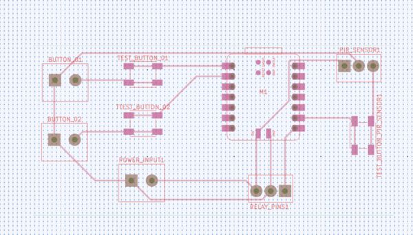
Layers .. The traces look correct, no overlapping
Black and white view of the board at the front
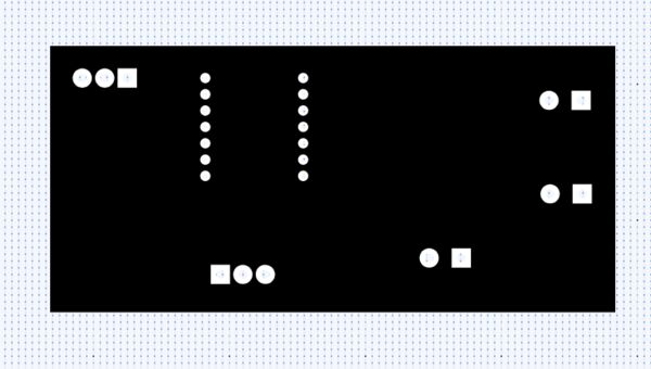
Black and white view of the board at the back
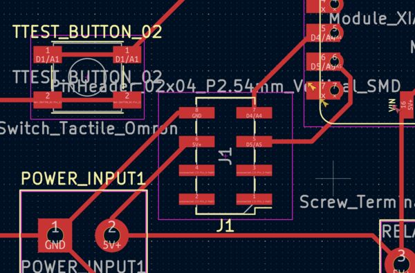
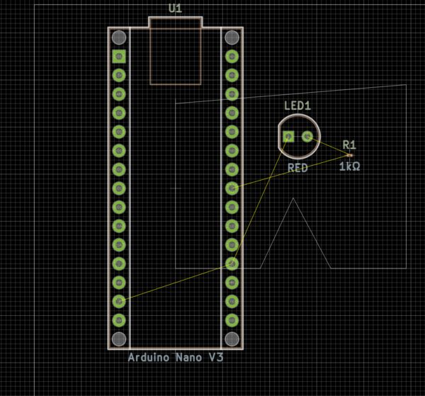
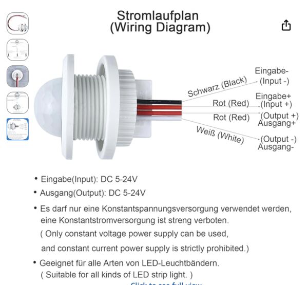
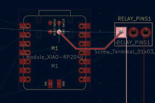
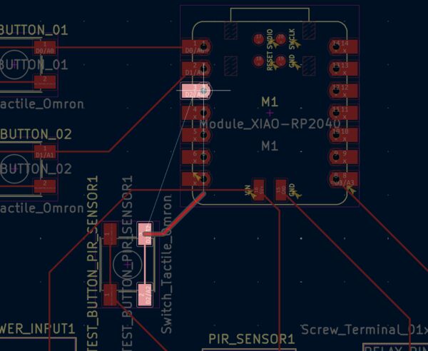
Extending design with I2C
Now that I have a PCB I want to extend with a I2C connector. I'm not sure what kind of device I want to use later on but what I can do (thx Henk for the tip) is to add connectors on my board for later use.
According to the wiki seeedstudio this requires 4 pins connected to GND, 5V+, D4 = SDA and D5 = SCL.
Note
I looked up the terminology related to I2C and picked a website. The I2C protocol involves using two lines to send and receive data: a serial clock pin (SCL) that the Arduino Controller board pulses at a regular interval, and a serial data pin (SDA) over which data is sent between the two devices.
Another protocol I can add is SPI. According to the wiki seeedstudio this requires, besides GND, 5V+, the use of pins connected to , D7, D8, D9 and D10.
Note
According to wiki is a de facto standard (with many variants) for synchronous serial communication, used primarily in embedded systems for short-distance wired communication between integrated circuits.
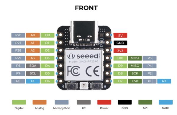
The color scheme shows quite nicely the pin layout for SPI, I2C (also IIC) and UART
So let's start with I2C ...
Time invested around 8 hours
Day 8 - [Wednesday]
Started around 08:30.
Extending design with I2C (part 2)
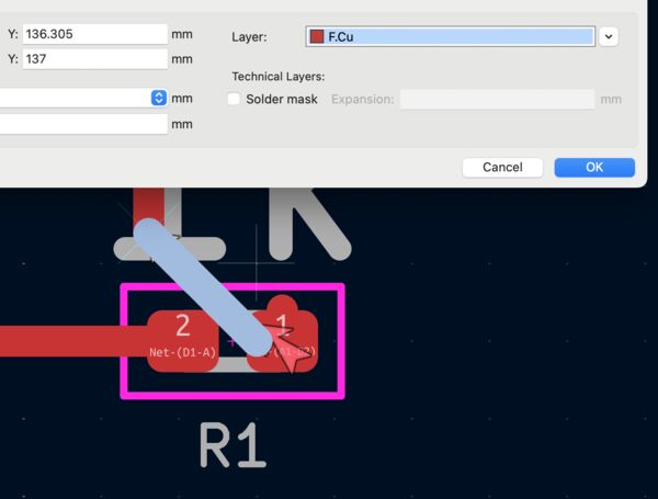
I continued and updated the board with the new pins. I saw that GND and 5V were crossed so I had to change them in the schematic editor. After updating the PCB again I now have added I2C connection to my board.
The only thing I don't like now is the fact that it show them lying on the PCB. I expected standing male pins.
I probably choose the wrong footprint in the schematic editor. So find a more suitable one. Well the no one in Kicad from the inventory list so I choose a standaard 8 male pin SMD. So why 8? Well my idea is thatt I2C and ISP can share the GND and 5V so that leaves me with 6 additional pins.
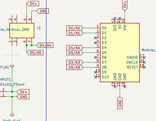
For now I only connected the I2C pins which resulted in
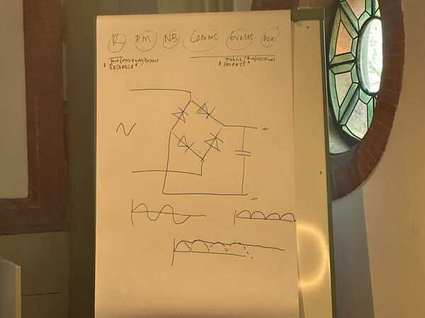
Simulation with EasyCircuit
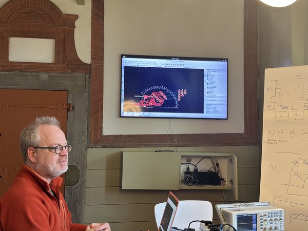
Almost time to finish up for the week because I also played around with EasyCircuit on my phone. Well they have a website as well but I did some transistor simulations in the train. It shows clearly that a transistor not only just switches current but also is able to regulate the flow from the collector to emittor (for this transistor that is).
I took 4 screenshots whereby I changed the voltage from 1V to 4V.
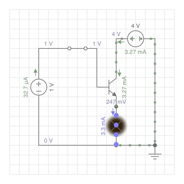
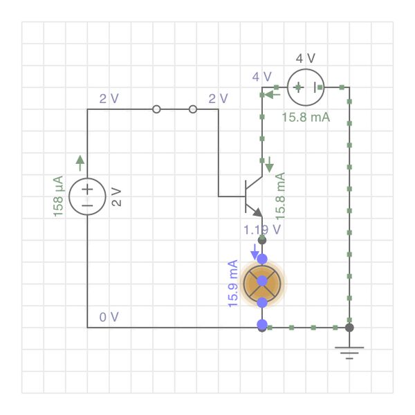
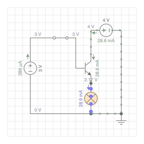
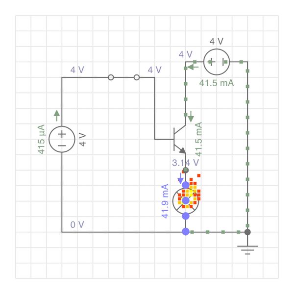
The screenshots only show a static result but I recreated this on their website as well and did a short recording so you get the idea.
So what I did was increase the voltage on the left side that regulates the transistor which makes the lamp turn brighter; powered by a 5V battery. But at a certain point when the regulation voltage is too high (around 6V) we see that no more current goes trough the lamp but makes a loop via de collector of the transistor. Really cool!!
Problems & Solutions
KiCad / PCB issues
- ERC errors (“input power pins not driven”) -> fixed by adding POWER_FLAG symbols to +5V and GND nets.
- Missing connections / nests not clearing -> found tiny unconnected vertical line; cleaned with “remove unconnected wires” tool.
- Footprint mismatch (through-hole terminals in 3D view) -> kept through-hole for prototyping reliability; plan to switch to SMD later.
- DRC explosion after stricter Waag rules (0.4 mm track/clearance) -> set net classes to 0.4 mm default width -> re-routed tight spots.
- Forgot Edge.Cuts outline -> added simple rectangle -> plotting worked.
Simulation-specific issues
- KiCad SPICE: no plots for LED circuit -> LED lacked model -> asked Grok to create one from datasheet -> attached .lib file -> ran DC sweep (0–5 V) -> got clean I–V curve.
- No graph data -> forgot to label nets (V_in, V_out) -> added labels -> plots appeared.
- EveryCircuit transistor circuit: lamp wouldn’t turn on -> base resistor too high -> lowered to ~1 kΩ + made pot interactive -> saw overdrive loop clearly.
- Falstad felt slow on mobile -> postponed deeper use; focused on two small analog experiments instead.
Files for Download / Replication
Please see the zip file.
Reflections & Learnings
What Went Well This Week
- Finally got comfortable iterating between schematic and PCB (update -> update PCB is now muscle memory)
- Gerber verification worked first try — very nice
- Adding I2C header after Henk's tip makes the board much more flexible
- I stayed more calm this week; "it will be alright" kind of mentality
What Was Challenging
- Understanding power flags + distinguishing real errors from warnings took longer than expected
- Footprint mismatches (through-hole vs SMD terminals) and 3D viewer surprises
- Balancing "good enough for this week" vs "perfect layout" — I still want nicer header orientation
What I Could Improve for Next Week(s)
- Have more fun & keep calm
Overall Lessons
Electronics design is really fun and more time consuming then I thought. A lot of time I spent with datasheets, cross-wiring, debugging etc... Documenting while doing (screenshots of every error) saved me hours reconstructing what I did. But I really like it
Link to Final Project
Indirectly I would say .. this board is to practice but I don't think I will use it later on. However, now I know how to make one Maybe created multiple specialsed boards for motor, visuals, location, game and let them 'talk' together via I2C?
References & Acknowledgements
Again I thank:
- Henk — for the focused local guidance, suggesting the 5 V PIR alternative, recommending I2C headers for future-proofing, and helping me refocus when I was over-engineering the redesign.
- Erwin Kooi (FabAcademy 2021) — excellent local tutor session on fundamentals (voltage/current analogies, flyback diodes, component basics). Your waterfall diagram and bridge-rectifier explanation finally made sense of capacitors and diodes.
- Heleen Emanuel and Remco van 't Veer — my Waag lab mates; doing the group work together
- Irja — your documentation helped me setup for Waag-specific DRC rules and net classes. And it all started with "are those lines not very small?"