What We Were Asked to Do
👥 Group Assignment
- Characterize the design rules for in-house PCB production — document machine settings
- Document the workflow for sending a PCB to a board house
- Reflect on the group work page
👤 Individual Assignment
- Make and test a microcontroller development board that you designed
From KiCad Design to Physical PCB
After designing the PCB in the Week 06 Electronics Design assignment, this week was about turning that design into a real, working board — milling it in-house, soldering the components, and testing it. The board is based on the XIAO ESP32-C3 with an SMD push button and a through-hole LED.
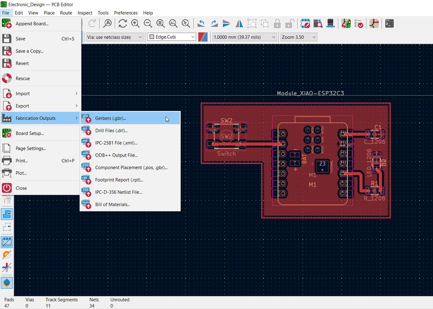
Exporting Gerber Files from KiCad
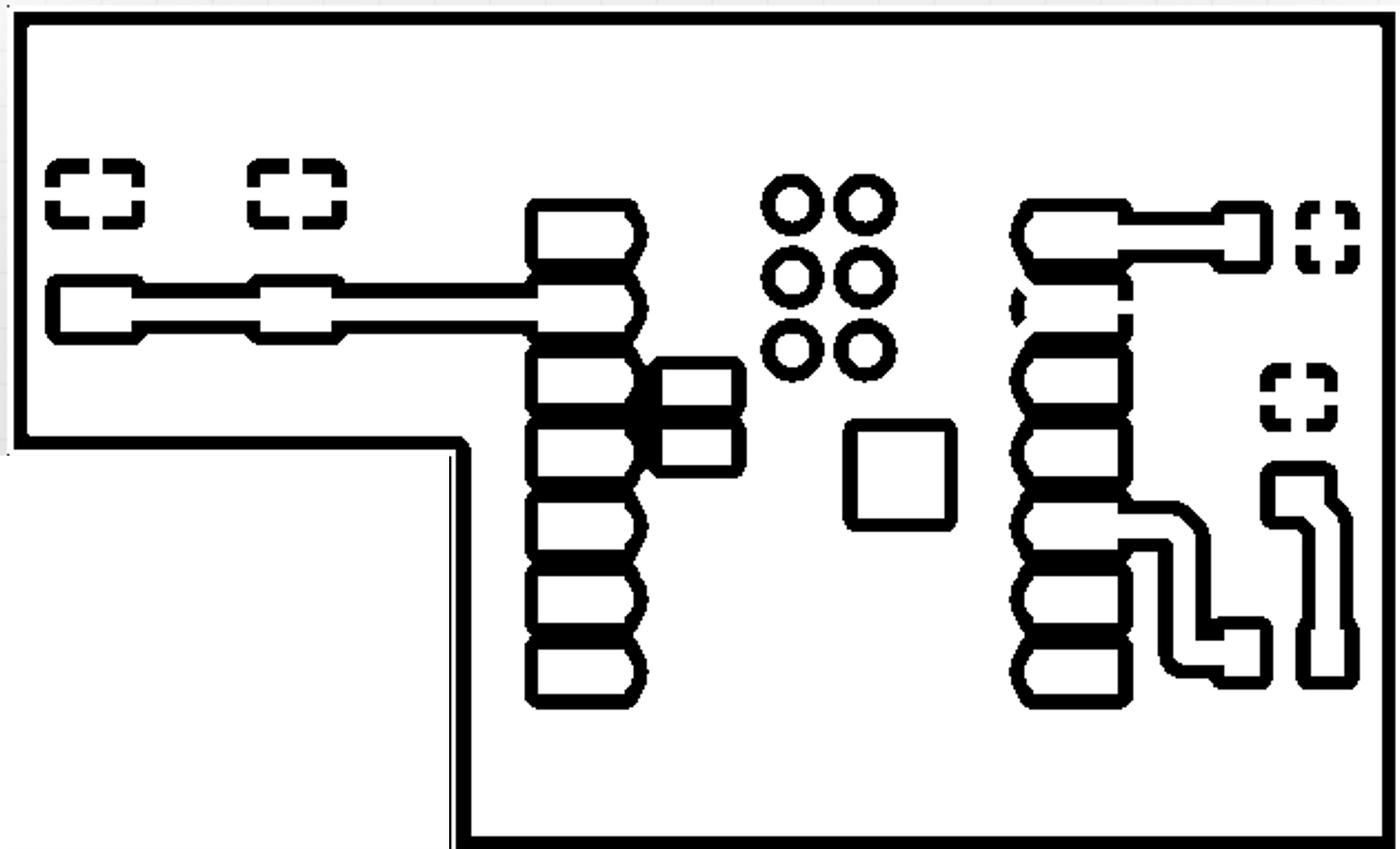
I started from my completed KiCad PCB design. To prepare it for fabrication, I went to File › Fabrication Outputs › Gerbers and selected the layers needed for in-house milling — F.Cu for the copper traces and Edge.Cuts for the board outline. I clicked Plot, then Generate Drill Files to produce the complete set.
Gerber to PNG with Gerber2PNG Plugin
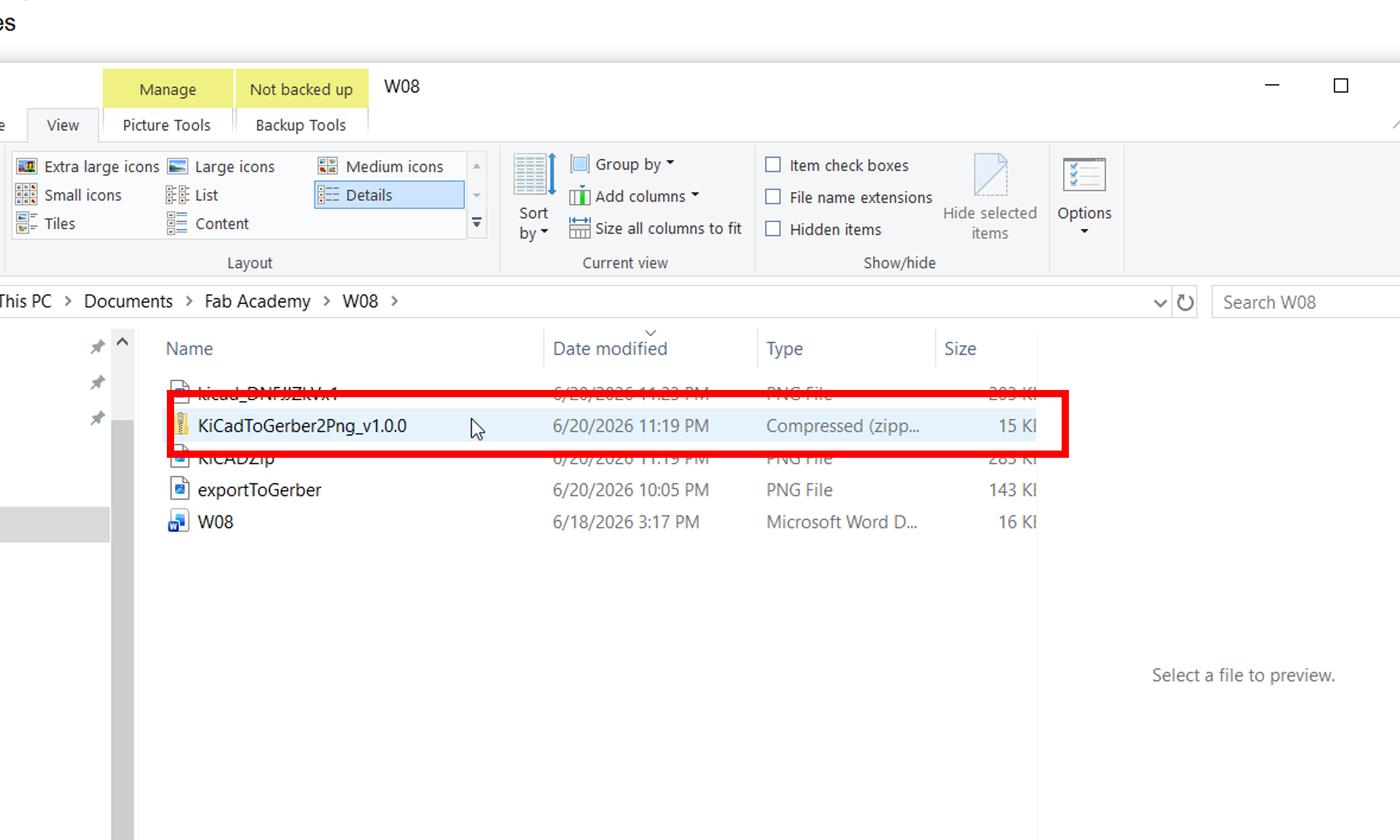
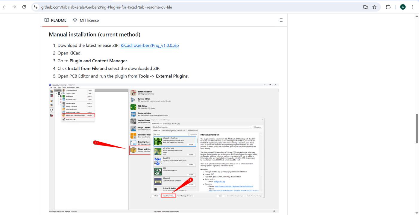
The PCB mill needs PNG image files, not Gerber files directly. Rather than using an external website, I used the Gerber2PNG plugin — created by Fab Lab Kerala — which converts Gerber outputs to PNG entirely within KiCad. I downloaded the plugin from the Fab Lab Kerala page in Git Hub. I followed the installing instructions in the page and installed it through KiCad's Plugin and Content Manager.
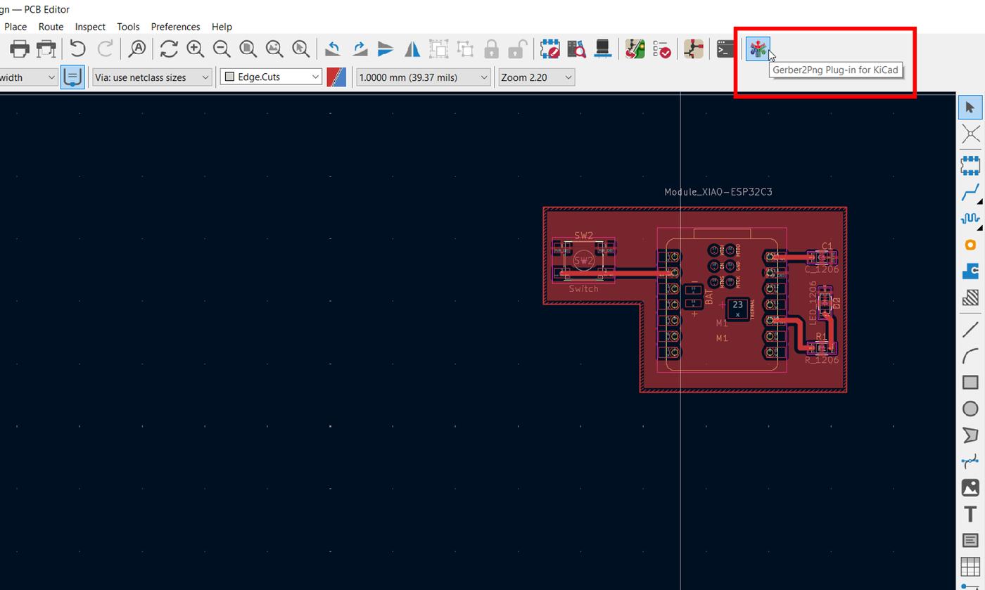
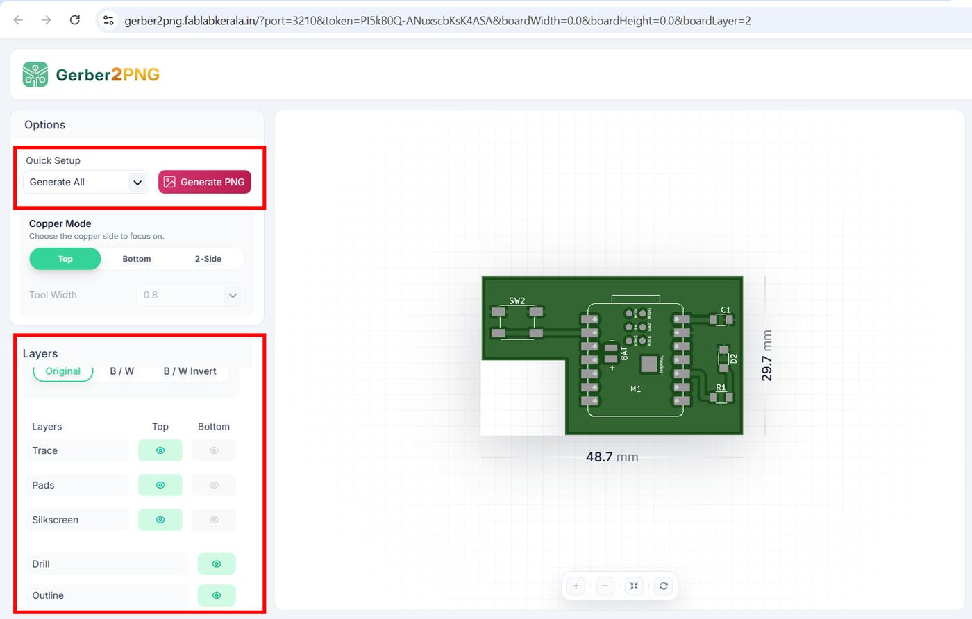
Once launched, I checked all three required layers and the plugin generated the PNG files:

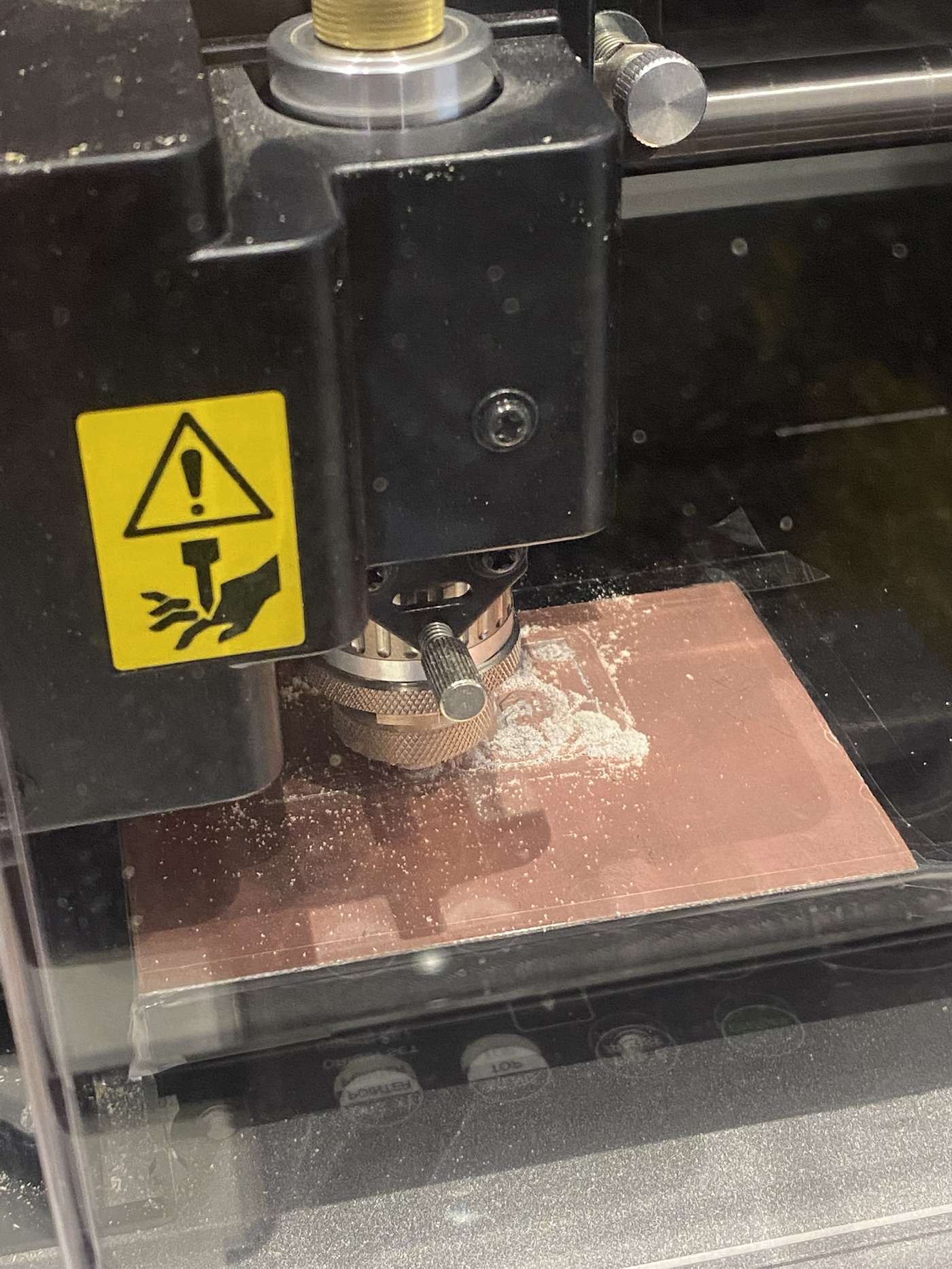
Milling the PCB
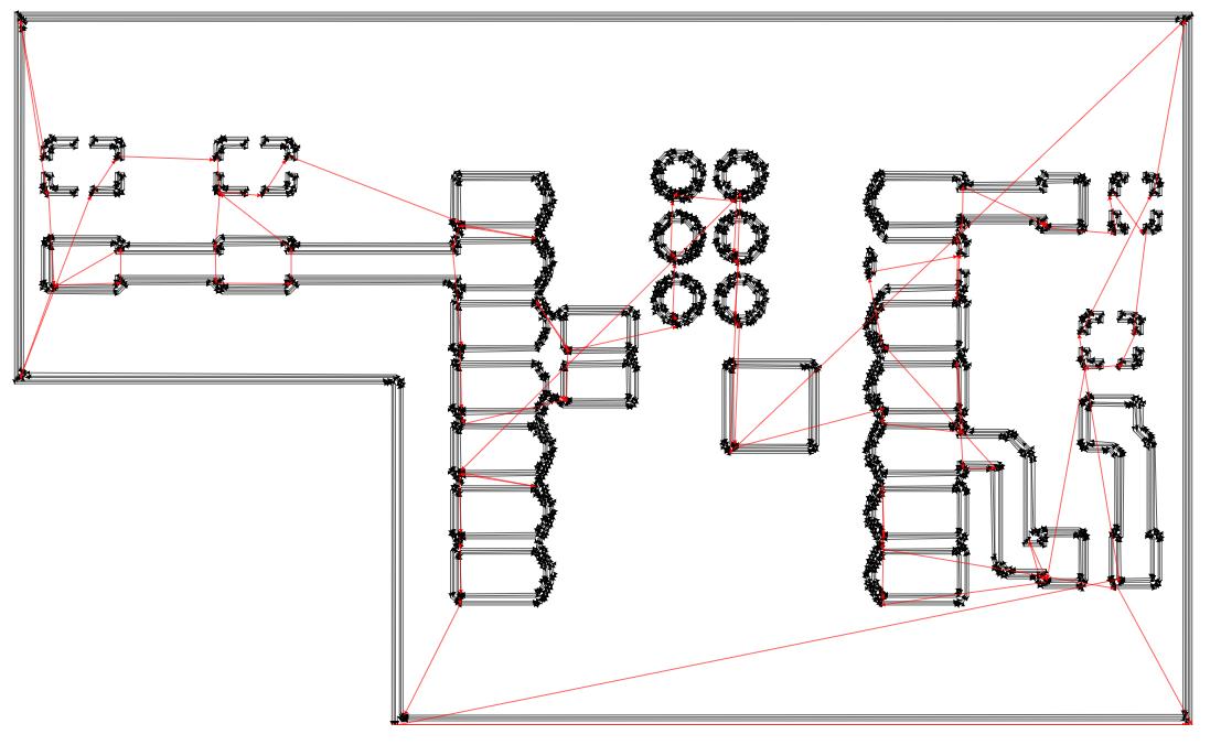
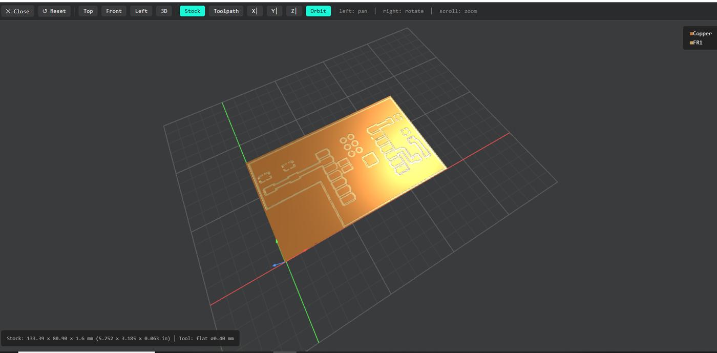
To generate the G-code I used the mods project web interface — a browser-based CAM tool that converts PNG files into toolpaths for the mill. I selected Programs → iModela mill → PCB from the left sidebar, then uploaded the trace PNG. The machine used is the Roland iModela.
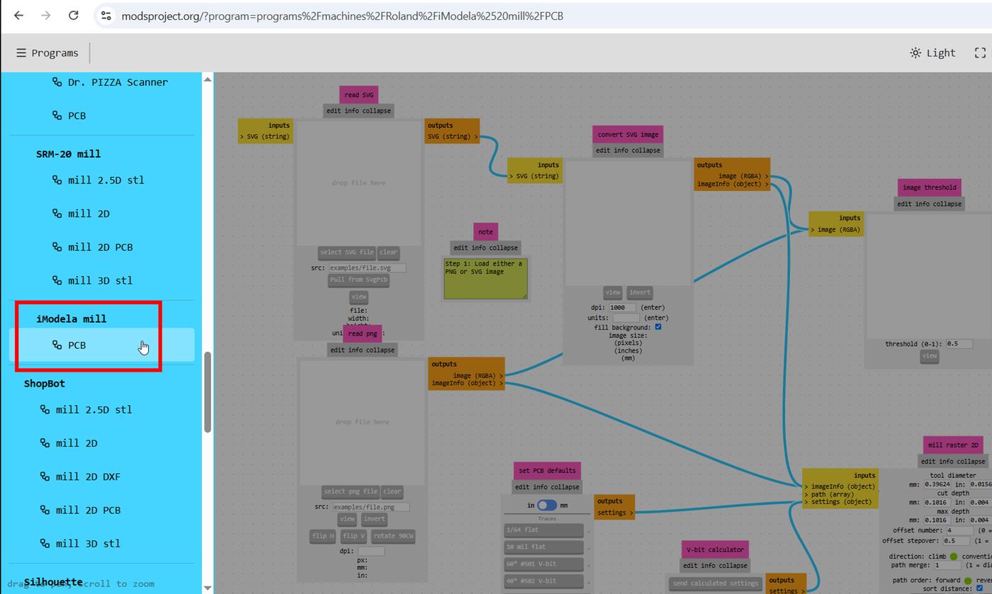
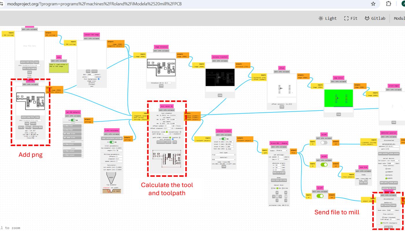
After uploading the PNG, mods calculates the toolpath using the parameters set in the mill raster 2D node. The following settings were used:
| Parameter | Value |
|---|---|
| Tool diameter | 0.40 mm |
| Cut depth | 0.10 mm |
| Max depth | 0.10 mm |
| Offset number | 4 |
| Offset stepover | 0.2 |
| Feed speed | 4 mm/s |
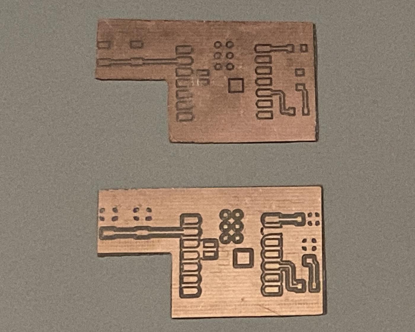
PCB Milling Errors & Re-Fabrication
The first milling attempt revealed two fabrication issues: the GND isolation path was accidentally closed on the first board, and the board outline was slightly misaligned. I corrected both issues and fabricated a new PCB. Both defects could lead to electrical or mechanical issues, so I discarded the board and re-milled a corrected version.
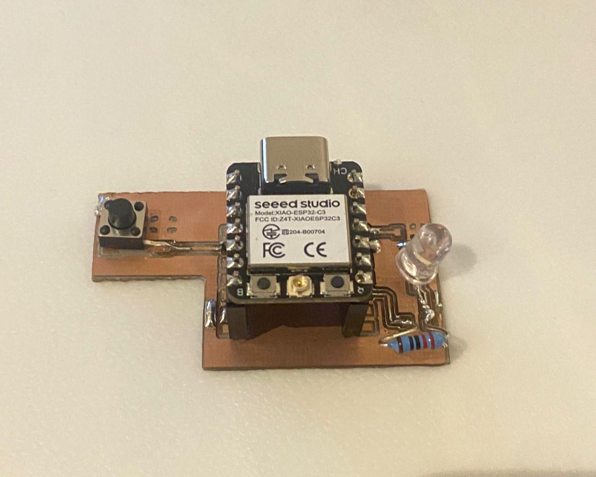
Soldering the Components
With the board milled and cut out, I soldered all the components. The board uses a mix of SMD and through-hole parts, which I placed and soldered in order of size — smallest SMD components first, then the through-hole LED, and the XIAO last.
Verifying the Board with a Multimeter
After soldering, I used a multimeter to verify the board electrically before connecting it to a computer. Two tests were performed: a continuity test to check for unintended bridges or open connections, and a voltage measurement to confirm the power rails were delivering the correct voltage once the board was powered.
Continuity Test
With the board unpowered, I placed the multimeter in continuity mode (beep mode) and probed across pairs of pads that should be connected — GND to GND, VCC rail to the XIAO's 3V3 pin — and also probed across pairs that must not be connected, such as adjacent signal pads and the GND pour versus signal traces. Any unintended beep would indicate a short. The test confirmed clean isolation between all signal nets and a solid, unbroken GND plane.
Continuity test — probing GND and signal pads for shorts and open connections
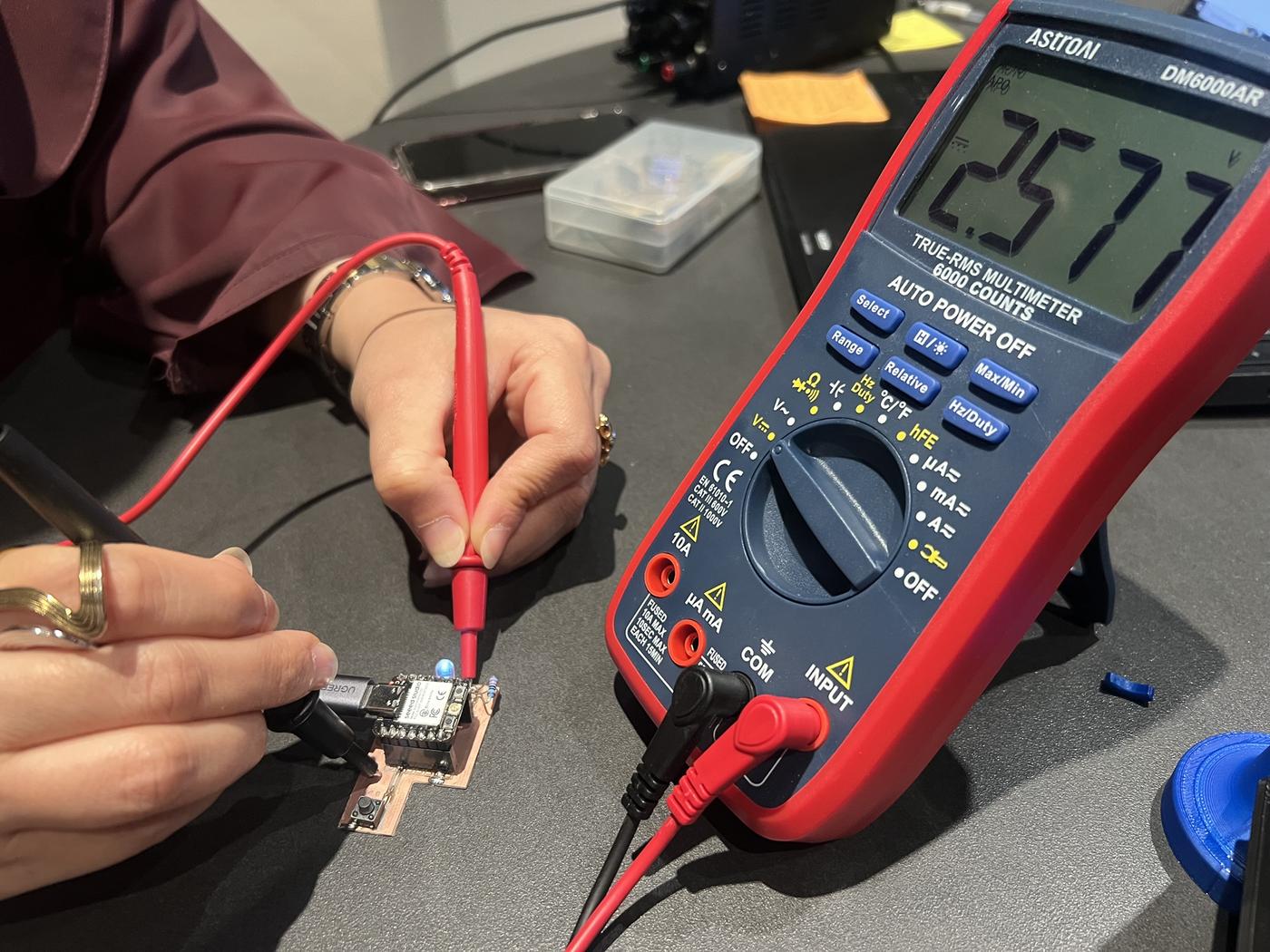
Voltage Measurement
With the board connected to USB power, I set the multimeter to DC voltage and measured across the 3.3 V power rail (XIAO 3V3 pin to GND). The reading was 2.577 V — close to the expected 3.3 V output. The slight drop is consistent with the internal LDO under light load and is within normal operating range for the ESP32-C3.
| Test | Method | Expected | Result | Pass? |
|---|---|---|---|---|
| GND continuity | Beep mode — GND pad to GND pour | Beep (connected) | Beep ✓ | ✅ |
| VCC-to-GND isolation | Beep mode — 3V3 rail to GND | No beep | Silent ✓ | ✅ |
| Signal trace isolation | Beep mode — adjacent pads | No beep | Silent ✓ | ✅ |
| 3.3 V rail voltage | DC V — 3V3 pin to GND | ~3.3 V | 2.577 V | ✅ |
Serial Monitor Output
Note on Test Context
This functional test was performed using the PCB fabricated for the Week 09 Input Devices assignment, which uses the same XIAO ESP32-C3 footprint and is electrically compatible with the button + LED circuit. It served as an initial end-to-end verification that the fabricated board could run firmware and communicate over serial — confirming the milling, soldering, and component placement were all correct. The complete firmware implementation and sensor analysis will be documented on the Week 09 page.
With the board flashed and running, I opened the Serial Monitor at 115200 baud. Pressing and releasing the button produced the expected log output — confirming the GPIO reads, LED control, and serial communication were all functioning correctly on the physical board.
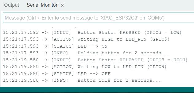
Each press-and-release cycle logged four lines: the GPIO state change, the write command sent to the LED pin, the resulting LED status, and a hold/idle timer. This confirmed that the board's input, output, and serial communication were all working correctly — a complete functional verification of the fabricated PCB. For the full implementation, code walkthrough, and sensor analysis, see the Week 09 page.
What I Learned
This week connected the full electronics workflow from file to physical board. The two milling failures were the most instructive part: the GND bridge was only caught by continuity testing — without it, I would have soldered a shorted board. Both fixes (re-zeroing between passes, increasing the offset count in mods) came from the CAM step, not the design, which showed me that milling parameters directly determine electrical correctness, not just surface finish.
Testing in order — continuity unpowered first, then voltage — proved to be the right approach. It caught defects early and confirmed the solder joints before any firmware was loaded. The 2.577 V rail reading was within normal LDO tolerance. The serial monitor test completed the verification, confirming that GPIO, LED control, and serial communication all worked on the physical board. Going forward, I'll run a continuity check before every soldering session and add dedicated test pads to future board revisions.