This Week's Assignments
Group Assignment
- Use lab test equipment to observe a microcontroller circuit (logic analyzer)
- Document findings on the group page
Individual Assignment
- Use an EDA tool to design a development board
- Use parts from the inventory that interact with a microcontroller
For the group assignment, refer to my colleague's documentation: Sarah Aldosary — W06 Group Work →
Designing a PCB in KiCad
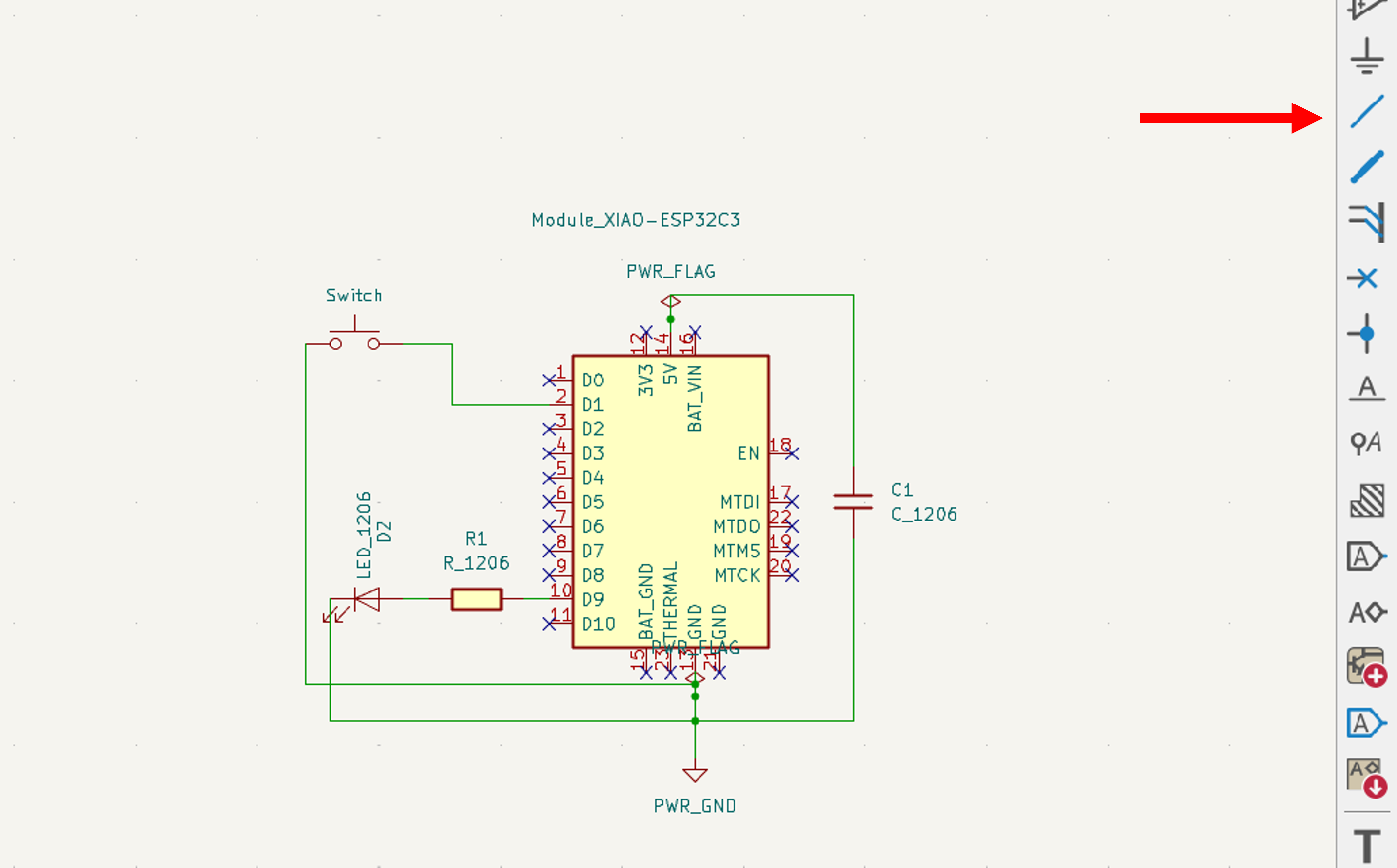
I wanted to approach this week as a genuine learning exercise, so I started small and deliberate. My goal was to design a simple development board featuring a XIAO ESP32-C3 with an LED, resistor, capacitor, and push button — enough components to practice the full EDA workflow from schematic to PCB layout.
I followed the Fab Academy KiCad tutorial throughout, which helped me understand not just the steps but the reasoning behind each one.
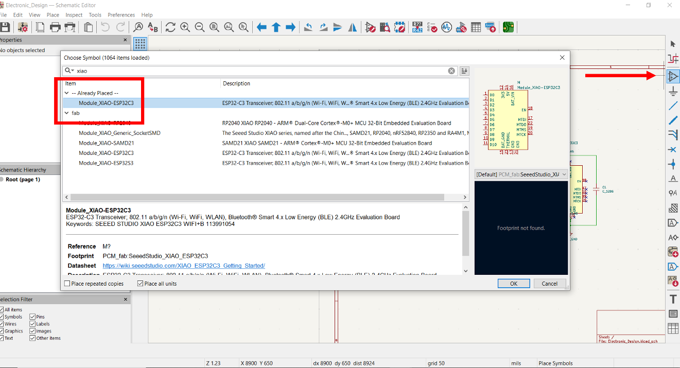
Installing the Fab Components Library
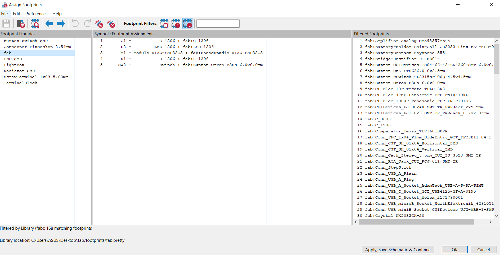
Before placing any components, I installed the Fab Academy component library into KiCad. This library contains footprints and symbols specifically selected for Fab Lab inventory — essential for ensuring the components I choose in the schematic will match what is physically available to fabricate with.
Placing Schematic Symbols
Using the Add Symbol tool, I placed the following components into the schematic editor:
- XIAO ESP32-C3 — the main microcontroller
- LED 1206 — surface-mount LED
- Resistor — current limiting for the LED
- Capacitor — decoupling for stable power
- Tactile switch button — user input
Wiring the Schematic
With all symbols placed, I connected them using the Draw Wire tool. The switch is wired to D1 and the LED is connected to D9, routed through the resistor and capacitor to the power rail.
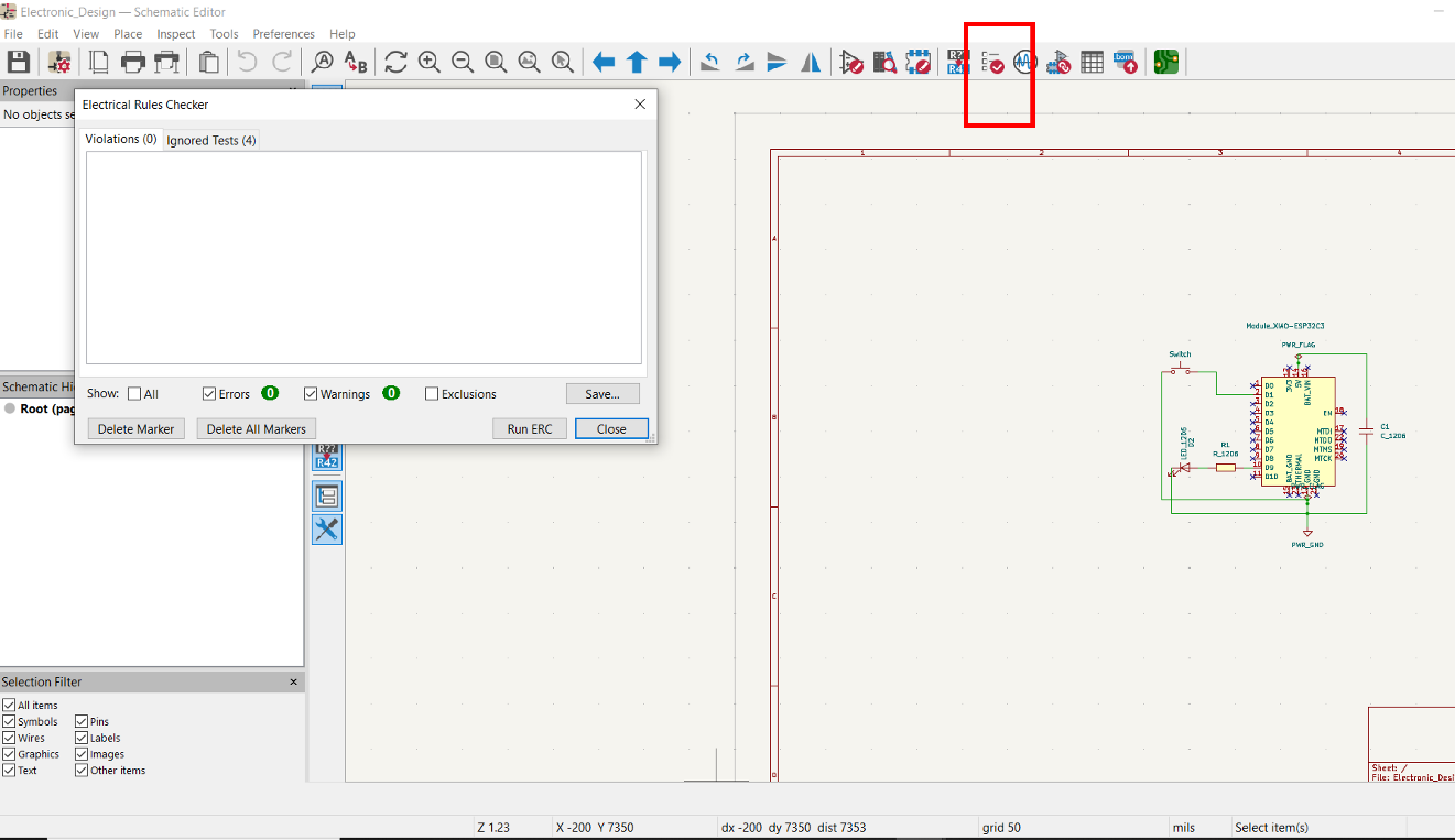
Running the Electrical Rules Check (ERC)
Before moving to PCB layout, I ran the Electrical Rules Checker from the top bar to catch any wiring errors — unconnected pins, missing power flags, or conflicting net assignments. Addressing these early prevents layout problems that are difficult to trace later.
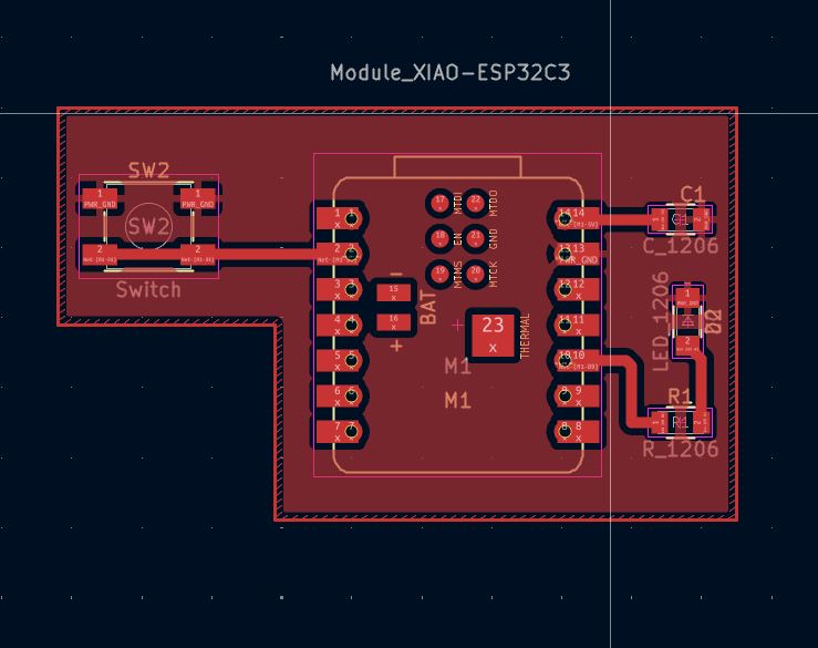
PCB Layout
I opened the PCB editor from Tools → Switch to PCB Editor and began placing and routing components. A few deliberate decisions shaped the layout:
- The button is placed at the board edge for easy thumb access
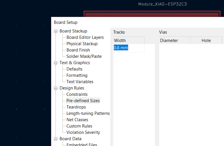
- Signal traces are set to 0.8 mm width to stay within CNC milling tolerances
- A ground fill on the bottom copper layer reduces noise and simplifies routing
What I Learned
This week gave me a clearer understanding of the full EDA workflow — from placing symbols and wiring a schematic, through footprint verification, to laying out and routing a PCB. What stood out most was how much easier the layout phase becomes when the schematic is clean and verified first.
Working with design rule constraints for CNC milling was also a useful insight: unlike fab-house PCBs that can handle 0.1 mm traces, milled boards require thinking about the physical limits of the cutting tool from the start. I'll carry that constraint forward into future designs.
Download KiCad Files
The complete KiCad project — schematic, PCB layout, netlist, and BOM — is available below.
⬇ Download KiCad Project (Electronic Design)