11 : Networking & Communications<
Learning Outcomes<
What did I learn this week ?
- General Theory :
- Networks topologies
- Osi model
- GPIO hardware
- UART :
- How a message is coded for UART
- I²C :
- How a message is coded for I²C
- Why a pull-up tension is required
Assignments<
This eleventh week's asignments are :
- Group :
- Send a message between two projects
- Individual :
- Design, build, and connect wired or wireless node(s) with network or bus addresses and local input &/or output device(s)
1. Theory<
1.1. General overview<
It has now been a few weeks that we started doing electronics for the Fab Academy. We learned :
- Week 4 : How to write and send instructions to a microcontroller in order to automate some tasks
- Week 6 : How to design an electronic board to easily connect a microcontroller to devices
- Week 8 : How to build an electronic board we designed
- Week 9 : How to measure something with a device connected to a microcontroller
- Week 10 : How to control a device with a microcontroller
During all these weeks I heard about some weird names such as UART or I²C. I understood these were methods to communicate with the microcontroller and I used them without really understanding how it works. Now is the time ! I will learn the basics of electronics communication and how I managed to talk with my microcontroller for all these weeks.
Digital signals : Bits<
You maybe heard this a lot, in the digital world, data are sequences 0 and 1. Indeed a computer or a microcontroller simply feels voltage therefore to send it a message one will have to translate it in voltage.
Historically, computers were invented to make computations (yes...) and it's been a reeeeaaaaally long time since humans try to do machines that compute. The idea that an efficient way to automate computations would use a binary digital system appeared few centuries before we discovered electricity (Leibniz according to Wikipedia). Indeed in a binary system, quite complex operations such as multiplications and divisions are simple additions and soustractions.
The first electrical computers were still made trying to use a decimal system (well... anthropocentrism) but it was quite hard and finally people went back to binary system which was way easier to electrically implement since one can associate 0 and 1 to HIGH and LOW voltage levels.
Quite rapidly people tried to use computers to communicate hence a code language to translate letters and words in a binary system was required. Therefore, a bit like Morse, code languages were invented to make each character, number and instructions equivalent to a sequence of HIGH and LOW voltage levels.
Network topology<
A set of communicating devices is called a network. The structure of the different communication lines between these devices is called the netwotk topology. Network topologies can be classified in two large categories :
-
Diffusion mode (Bus or ring topologies) : Only one large communication line connecting all the devices is used. The message is sent on the whole network and all the devices are able to see the message. An adress system is used for the devices to recognize if the message is meant for them.
-
Point-to-point mode (Star or mesh topologies): Several communication lines are used and each one connect only two devices. There is thus no need for an adress system.
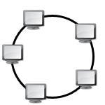
Ring topology<
Devices are connected in a chain and each one of them play a intermediary role. When a message arrive to a device it reads it, interprets it and resends it in necessary. The inconvenient of such a topology is that a failing device or communication line breaks the whole network.
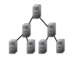
Tree topology<
The tree topology is divided in levels where each device is connected to one parent and several children. The inconvenient of such a topology is that a failing device or communication line blocks all communication to the lower levels.
Bus topology<
Devices are connected all passively connected to a same communication line which means they do not interfere with the communication when they read a message (the signal is "copied towards them"). Therefore a failing device has no impact on the rest of the network. However a failing communication line breaks the whole network.

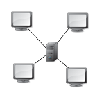
Star topology<
Devices are all connected to a central device called a hub where all communication go through. The hub is hence a major point of failure but if any other device fails, it will have to impact on the rest of the network.
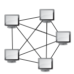
Mesh topology<
Devices are all connected together by point-to-point communication lines. If any device fails, it has no impact on the rest of the network however it requires a lot of communication lines.
Serial and Parrallel communication<
In this documentation, I will only learn about serial communication which is the simplest way to imagine communication : bits are sent one after another trhough one communication line from a device to another. The alternative is parallel communication where many bits could be sent at the same time from a device to another using several different communication lines.
Communication Protocol<
A communication protocol is a set of rules defined to allow communication between two devices. Communication generally requires a lot of different steps to transform a message into electrical current (and sometimes into electromagnetic waves) that can then be re-translated into a message. The rules of these steps may differ from one protocol to another however the OSI model suggests that each each protocol can be decomposed in layers :
- 7: Application (HTTP)
- 6: Presentation (SSL)
- 5: Session (RPC)
- 4: Transport (TCP, UDP)
- 3: Network (IP)
- 2: Linking (MAC)
- 1: Physical (PHY)
Note that these are all the possible layers but a protocol may only have some of them. In fact, in this documentation, we will only cover some wired communication protocols which are only concerned by the two first layers :
-
Physical rules :
- Physical definition of a bit (if digital signal)
- Electrical design of the ports required on the device
- Material design of the communication lines between the devices
- ...
-
Linking rules :
- Instructions to indicate when the message starts or stops
- The message itself
- The adress of the aimed device if needed
- ...
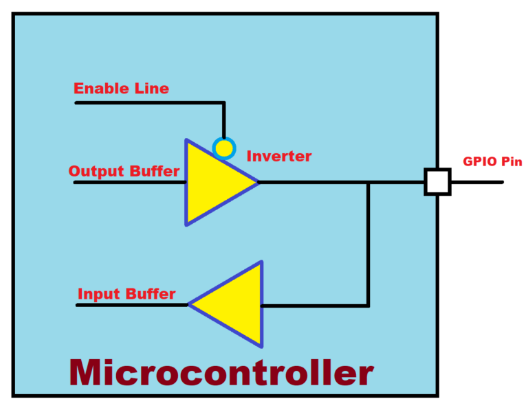
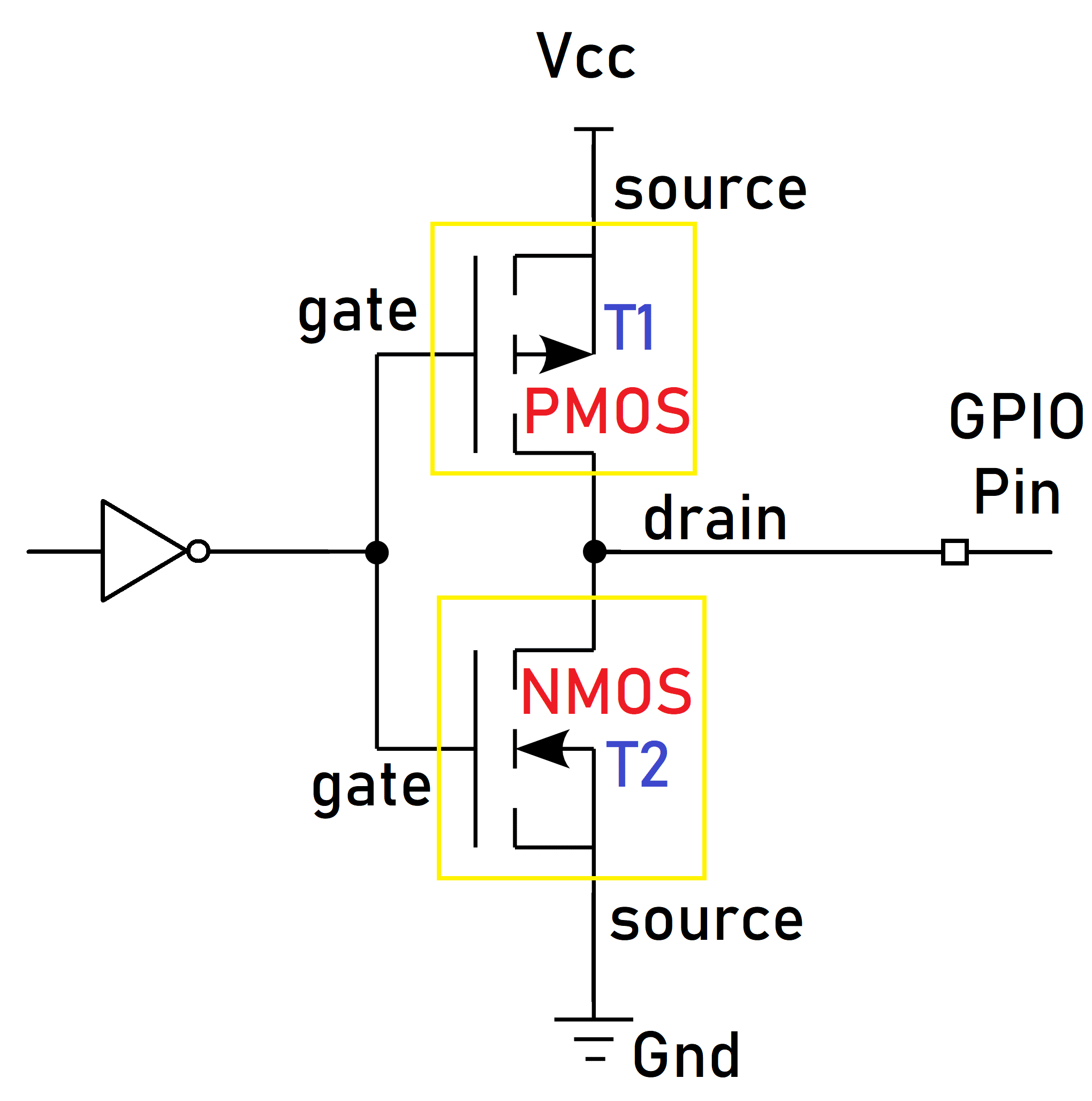
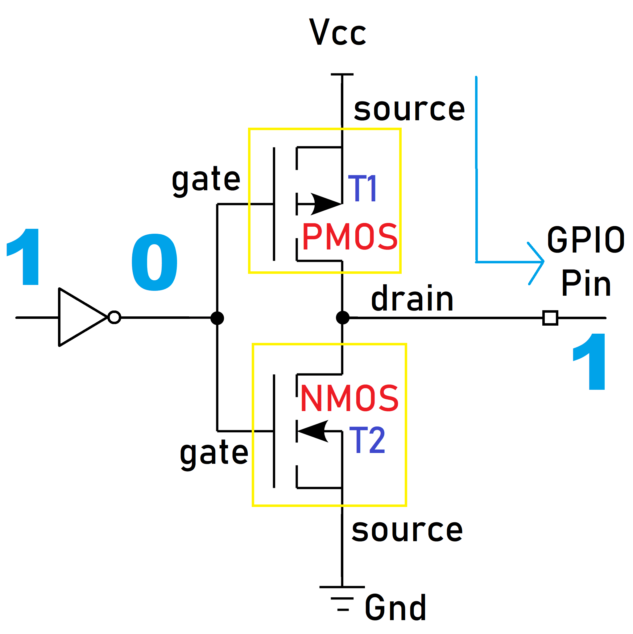
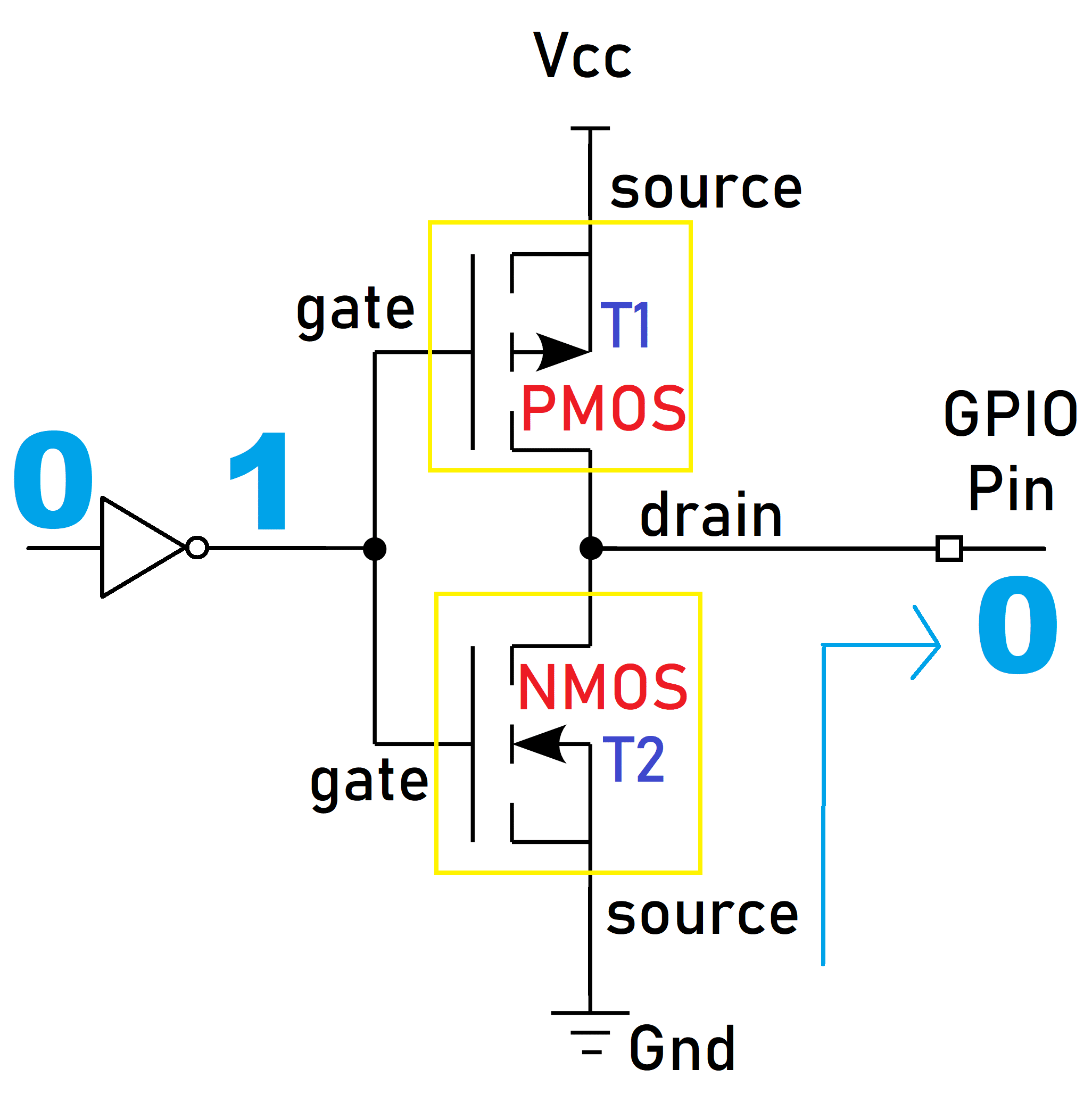
General Purpose Input Output (GPIO)<
Before going into specific protocols, I will explain what I learned about "General Purpose Input Output" ports or GPIO ports. The latter are a kind of pin that one can find on any microcontroller and that can be used as well as inputs or outputs.
Note
Understanding GPIO is required do understand the physical layer of the communication protocol that I present in the next sections. However one may skip GPIO to undertsand only the linking layer.
Understanding GPIO may also give you a better insight about how can a microcontroller generate 1's and 0's as much as read 1's and 0's.
A general GPIO port can be schematized as below. We will explain further what are the input and output buffers.
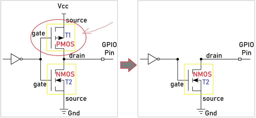
Push-Pull<
Open-drain<
1.2. UART<
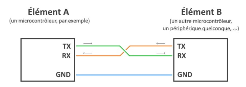
The UART protocol is the acronym of "Universal Asynchronous Receiver Transmitter". It is a point-to-point communication protocol hence it can connect two and only two devices however it is bidirectionnal meaning that both devices can send/receive data to/from each other.
Physical<
Wires<
Its communication line is made of three wires :
- Device A to Device B wire
- Device B to Device A wire
- Ground wire, to ensure equipotentiality
Common mistake
Be carefull, the wires must be inverted between the RX and TX pins of both device. Indeed data must be sent from a transmission pin (TX) and arrive to a reception pin (RX).
Note that the two communication wires are independant which means both of them can carry data at the same time without any synchronization required (hence the word asynchronous).
Pins<
On both devices, UART ports thus require :
- Transmission pin, TX
- Reception pin, RX
- Ground pin
RX and TX pins are both push-pull GPIO respectively in input and output modes.
Link<
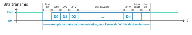
As explained in the introduction, data are a sequence of 0's and 1's physically corresponding to a sequence oh HIGH and LOW voltage levels. By default, when the line is not transmitting anything, it is on a HIGH voltage level.
Data are sent one bit at a time (serial communication) and are sequenced as below :
- Start bit : Forced LOW voltage level to indicate communication is starting
- Data bits : The message or a part of the message as a sequence of 5 to 9 bits maximum
- Parity bit (optional) : Optional bit used to detect error. It indicates the parity of the number of HIGH or LOW levels, comparing this bit to the message can help one to detect errors.
- Stop bit : Forced HIGH voltage level to indicate communcation is ending
The duration of a bit depends on the communication speed. The most commonly used is 9600 bauds (corresponding to 9600 bits/s). Below you may find a graphical representation of a typical UART sequence.
1.3. I²C<
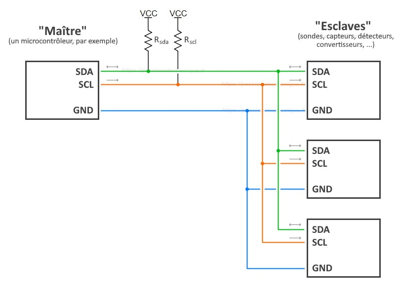
The I²C protocol is the acronym of "Inter Integrated Circuit". It is a diffusion communication protocol hence it can connect several devices on the same communication line however an adress system is required for the devices to recognize if the message is meant for them.
It is bidirectonal meaning that each device can send and receive data. Therefore, to avoid data collision, the I²C protocol uses the master/slave system where only one device called the master can decide when and which device can send data. We call an I²C bus any network using the I²C protocol.
Physical<
Wires<
Its communication line is made of three wires :
- SDA wire : bidirectional Serial DAta line containing the data
- SCL wire : Serial CLock line synchronizing the data coming from all devices
- Ground wire : ensuring equipotentiality
Pins<
On both devices, I²C ports thus require :
- SDA pin, receiving and transmitting data
- SCL pin, synchronizing data
- Ground pin
You may have noticed resistance connecting the SDA and SCL lines to the power tension. These are pull-up resistance required to avoid tension conflicts on the line.
Link<
2. Individual Assignment<
OLED screen with AtTiny412
2.1. Scanning I²C devices<
#include <Wire.h>

void setup() {
  Wire.begin();
  Serial.begin(9600);
  Serial.println("Scanning for I2C devices...");
  for (byte i = 1; i < 127; i++) {
    Wire.beginTransmission(i);
    if (Wire.endTransmission() == 0) {
      Serial.print("I2C device found at address 0x");
      Serial.println(i, HEX);
    }
  }
}

void loop() {}
Output
~pce found at address 0x1E
I2C device found at address 0x1F
I2C device found at address 0x20
I2C device found at address 0x21
I2C device found at address 0x22
I2C device found at address 0x23
I2C device found at address 0x24
I2C device found at address 0x25
I2C device found at address 0x26
I2C device found at address 0x27
I2C device found at address 0x28
I2C device found at address 0x29
I2C device found at address 0x2A
I2C device found at address 0x2B
I2C device found at address 0x2C
I2C device found at address 0x2D
I2C device found at address 0x2E
I2C device found at address 0x2F
I2C device found at address 0x30
I2C device found at address 0x31
I2C device found at address 0x32
I2C device found at address 0x33
I2C device found at address 0x34
I2C device found at address 0x35
I2C device found at address 0x36
I2C device found at address 0x37
I2C device found at address 0x38
I2C device found at address 0x39
I2C device found at address 0x3A
I2C device found at address 0x3B
I2C device found at address 0x3C
I2C device found at address 0x3D
I2C device found at address 0x3E
I2C device found at address 0x3F
I2C device found at address 0x40
I2C device found at address 0x41
I2C device found at address 0x42
I2C device found at address 0x43
I2C device found at address 0x44
I2C device found at address 0x45
I2C device found at address 0x46
I2C device found at address 0x47
I2C device found at address 0x48
I2C device found at address 0x49
I2C device found at address 0x4A
I2C device found at address 0x4B
I2C device found at address 0x4C
I2C device found at address 0x4D
I2C device found at address 0x4E
I2C device found at address 0x4F
I2C device found at address 0x50
I2C device found at address 0x51
I2C device found at address 0x52
I2C device found at address 0x53
I2C device found at address 0x54
I2C device found at address 0x55
I2C device found at address 0x56
I2C device found at address 0x57
I2C device found at address 0x58
I2C device found at address 0x59
I2C device found at address 0x5A
I2C device found at address 0x5B
I2C device found at address 0x5C
I2C device found at address 0x5D
I2C device found at address 0x5E
I2C device found at address 0x5F
I2C device found at address 0x60
I2C device found at address 0x61
I2C device found at address 0x62
I2C device found at address 0x63
I2C device found at address 0x64
I2C device found at address 0x65
I2C device found at address 0x66
I2C device found at address 0x67
I2C device found at address 0x68
I2C device found at address 0x69
I2C device found at address 0x6A
I2C device found at address 0x6B
I2C device found at address 0x6C
I2C device found at address 0x6D
I2C device found at address 0x6E
I2C device found at address 0x6F
I2C device found at address 0x70
I2C device found at address 0x71
I2C device found at address 0x72
I2C device found at address 0x73
I2C device found at address 0x74
I2C device found at address 0x75
I2C device found at address 0x76
I2C device found at address 0x77
I2C device found at address 0x78
I2C device found at address 0x79
I2C device found at address 0x7A
I2C device found at address 0x7B
I2C device found at address 0x7C
I2C device found at address 0x7D
I2C device found at address 0x7E