Electronics Design
Week 6
The objective of this assignment is to use an EDA tool to design a custom development board that integrates components from the lab inventory. The board must be capable of interacting and communicating with an embedded microcontroller.
This week, I used two different software platforms to simulate electronic circuits: Altium Designer and NI Multisim. In Altium, I simulated a non-inverting operational amplifier, while in Multisim, I simulated a diode bridge rectifier.
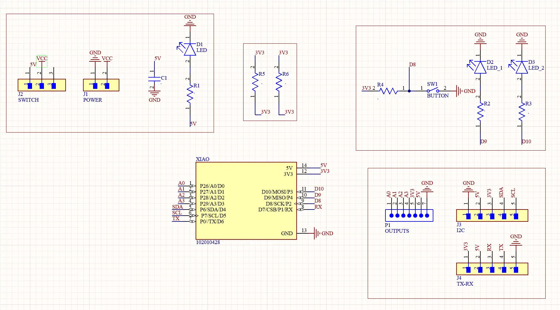
In addition, I designed a custom PCB specifically made for the XIAO ESP32-C3 microcontroller. I developed this board in Altium. The PCB features:
- Interactive Components: Programmable LEDs and push buttons.
- Communication: Headers for I2C and UART (TX/RX) protocols.
- I/O & Power: Outputs for programming and specific input pins for the power supply.
Group Assignment
Check here the
group assignment for this week for more information about electronic measure tools.
Simulation
Altium Designer
Altium Designer is a powerful EDA software that allows for complex circuit design and simulation. I used it to create a non-inverting operational amplifier circuit. To simulate a circuit in Altium, you can follow these steps:
Mixed Simulation
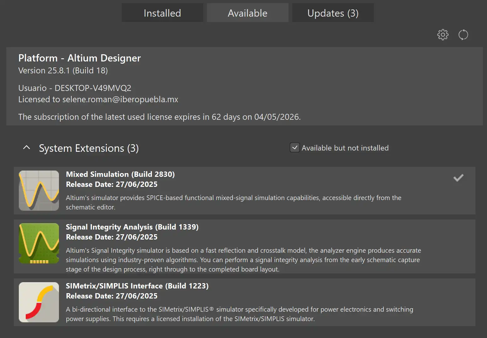
To start a new simulation project you must have the Mixed Simulation extension installed. In your profile go to "Extensions and Updates", search for "Mixed Simulation" and install it.
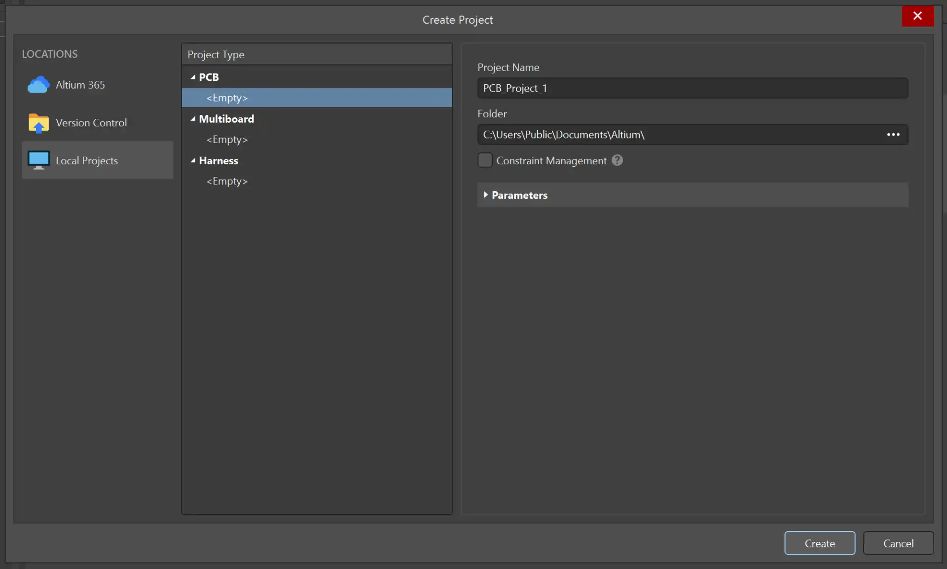
Create a Project
To start a new simulation project, go to File > New > Project. Name your project and save it.

Schematic
In the project, click with the right mouse button and select "Add New to Project" > Schematic. This will create a new schematic file where you can design your circuit.
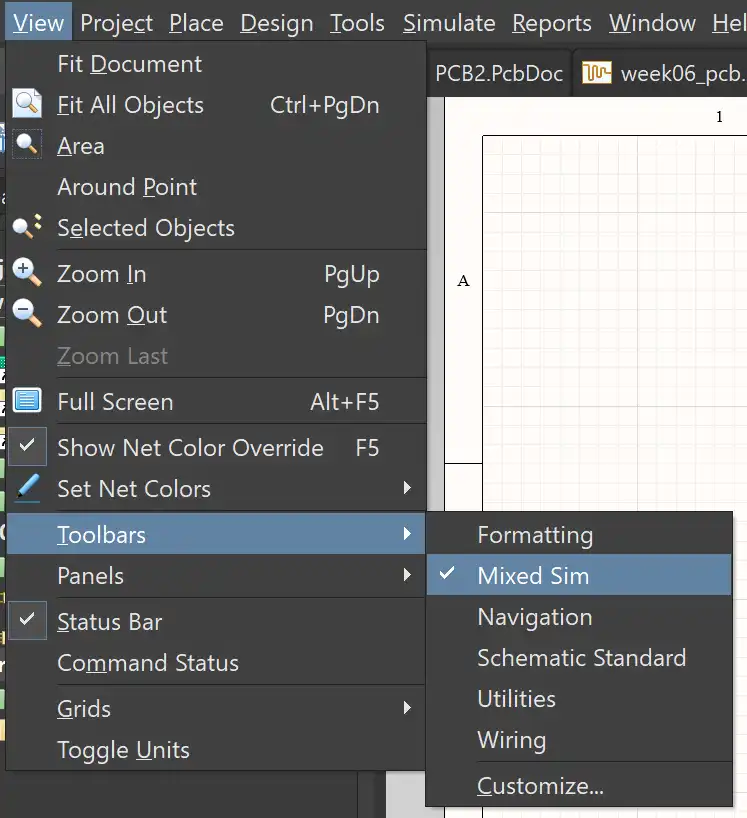
Toolbar
To activate the Mixed Simulation menu, go to View > Toolbars and check "Mixed Sim".
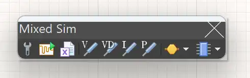
Mixed Sim
In the Mixed Simulation menu, you can find different tools to create your circuit. You can add power sources, components, and measurement tools. You can also adjust the simulation settings and run the simulation to see the results.
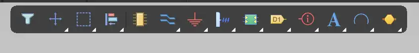
Toolbar
In the top toolbar, you cand find different tools to connect your components, add wires, and create buses. You can also find tools to add text and labels to your schematic to make it more organized and easier to understand.
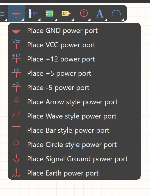
Power port
You can find different types of power ports in this menu to add to your schematic.
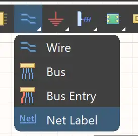
Net Label
To make your schematic more organized, you can use net labels, instead of wires, to name the different connections in your circuit. This will help you identify different nodes and make it easier to understand the circuit.
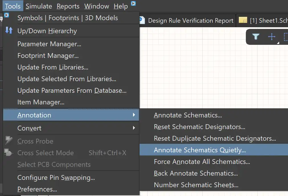
Annotation
Before running the simulation, you need to annotate your schematic. This process assigns a unique identifier to each component in your circuit, which is essential for accurate simulation results. To annotate, go to Tools > Annotation > Annotate Schematics Quietly.
Simultion Dashboard
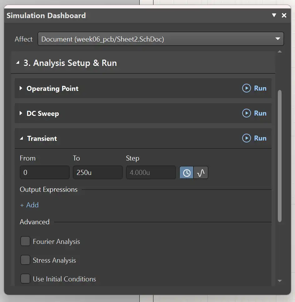
Once your circuit is ready, you can adjust the simulation settings by clicking on the wrench button in the Mixed Sim toolbar. Here you can set the type of analysis (transient, AC, DC, etc.) and adjust its parameters. I selected the Transient analysis and adjusted the time range From 0 To 250u and a Step of 4u.
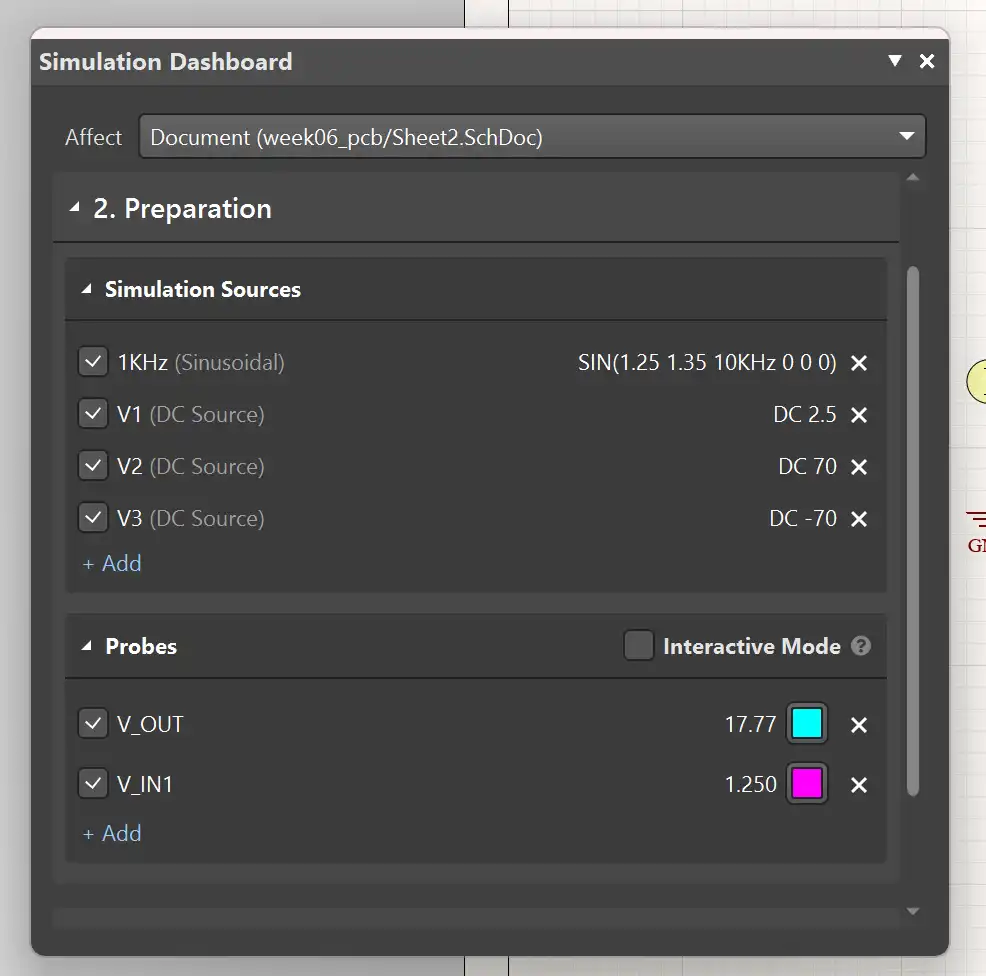
Probes
You can also add probes to your circuit to measure different parameters. In the Mixed Sim toolbar, you can find voltage, current, and power probes. Place them in your circuit where you want to take measurements. I placed two voltage probes, one at the input and another at the output of the operational amplifier.
Run Simulation
To run the simulation, click on the green play button in the Mixed Sim toolbar. This will open the simulation results dashboard where you can analyze the behavior of your circuit. You can view different graphs and measurements based on the probes you placed in your schematic.
❮
❯
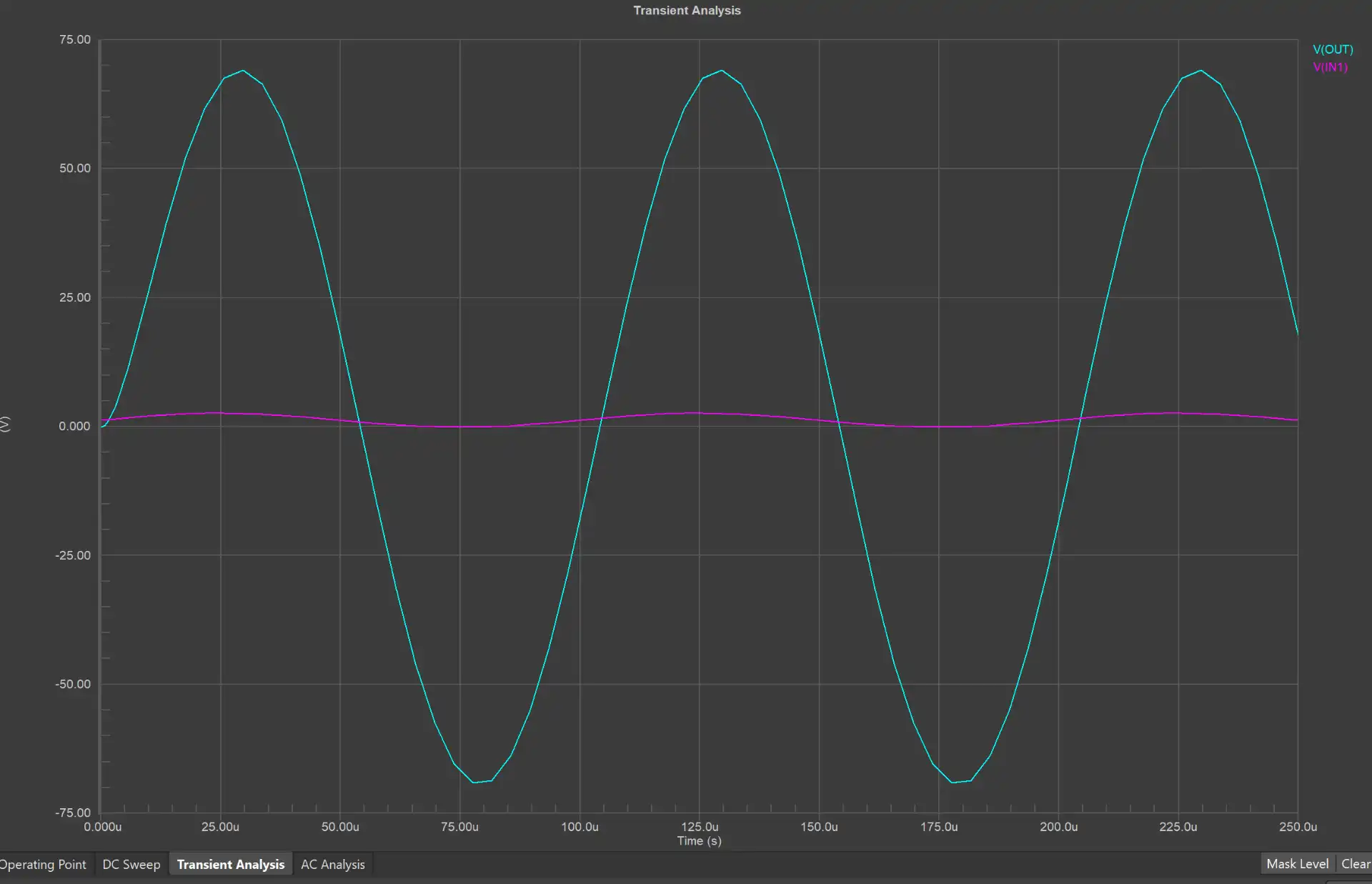
Here are the results of the simulation in Altium.
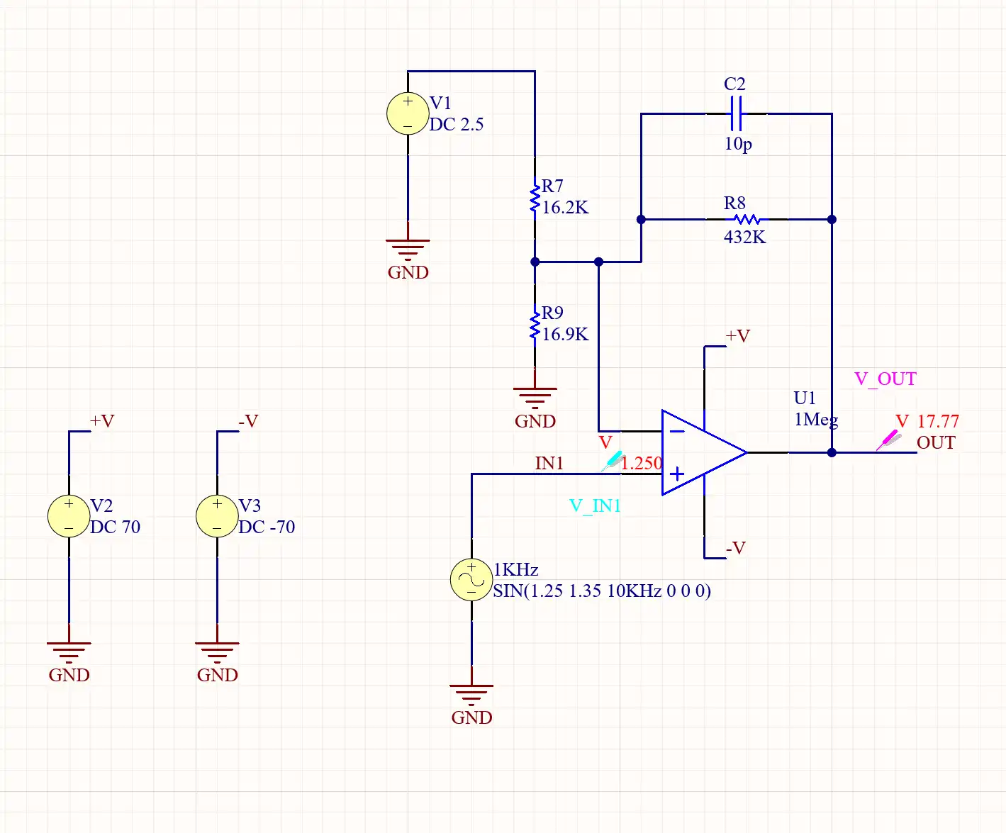 Fig 1. Simulation Circuit - Altium
Fig 2. Simulation Graph - Altium
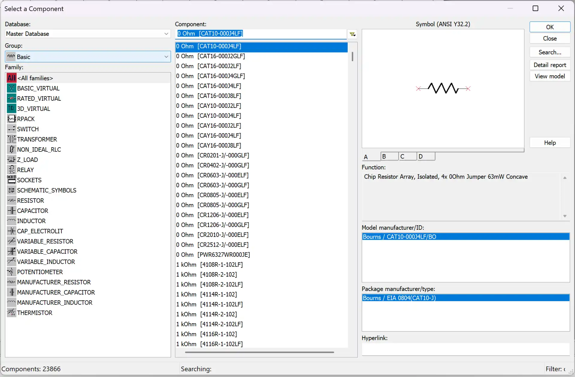
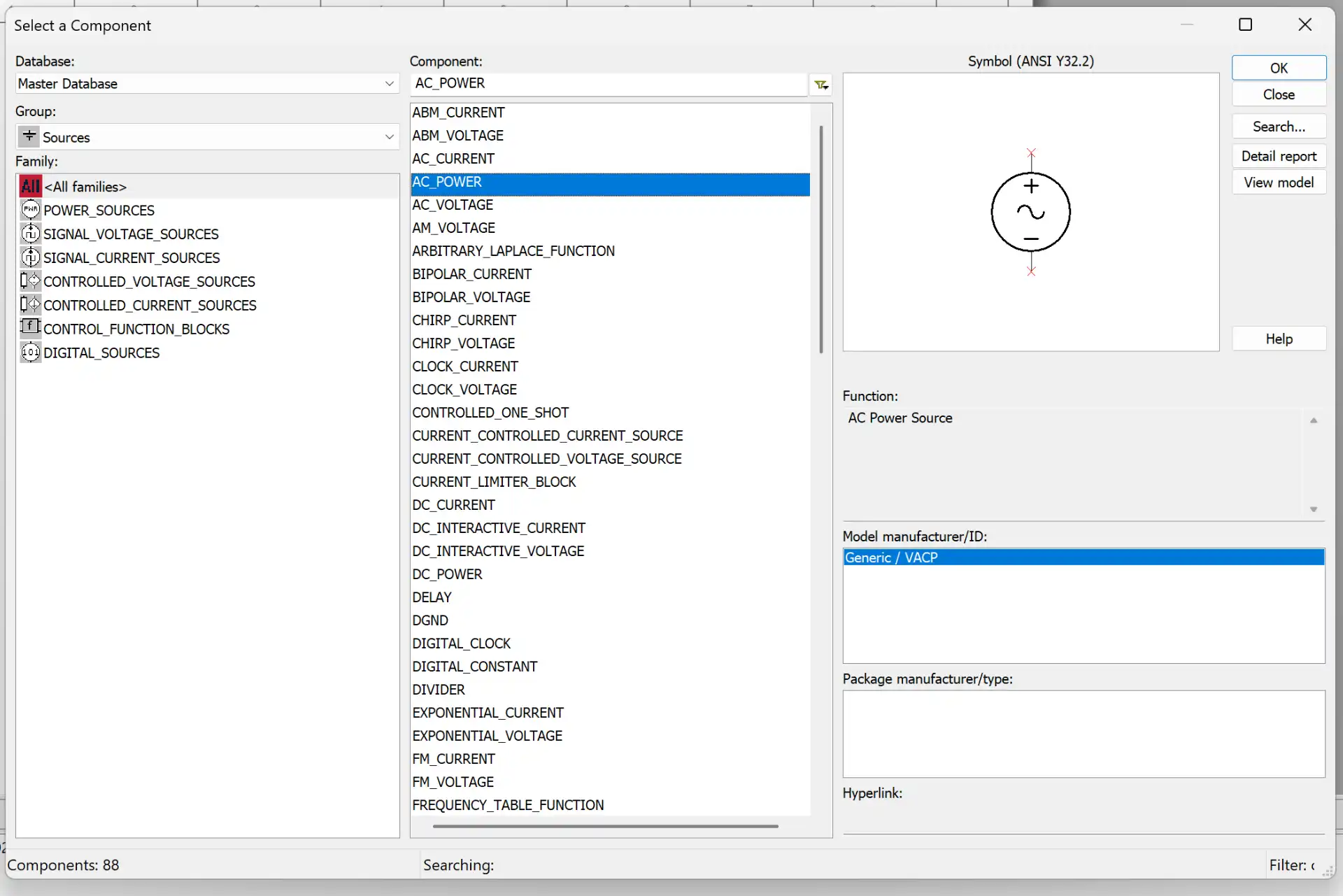
NI Multisim
NI Multisim is another popular EDA software that is widely used for circuit simulation and analysis. I used it to simulate a diode bridge rectifier circuit. You can follow these steps to simulate a circuit in Multisim:
Start
To start a simulation project, create a new document and you will see the main screen. In Multisim, you can find a wide range of components. You can search for specific components or browse through different categories to find what you need in the menu on the upper left corner.
Components
In the component menu, you can find different groups of components, you can also search for specific components using the search bar.
Select
Once you find the component you need, click OK and place it in your workspace. You can rotate the component by right-clicking on it and selecting "Rotate".
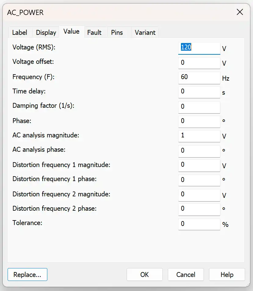
Properties
You can also adjust its value on the properties of the component by double-clicking on it.
Instruments
In the menu on the right side, you can find different instruments to measure the behavior of your circuit. You can add oscilloscopes, multimeters, and other measurement tools to your workspace.
Simulation
To run the simulation, click on the green play button on the top toolbar. This will start the simulation and you can see the results in the instruments you placed in your workspace. To make adjustments to your circuit, simply stop the simulation, make the necessary changes, and run it again to see the updated results.
❮
❯
Here are the results of the simulation in Multisim.
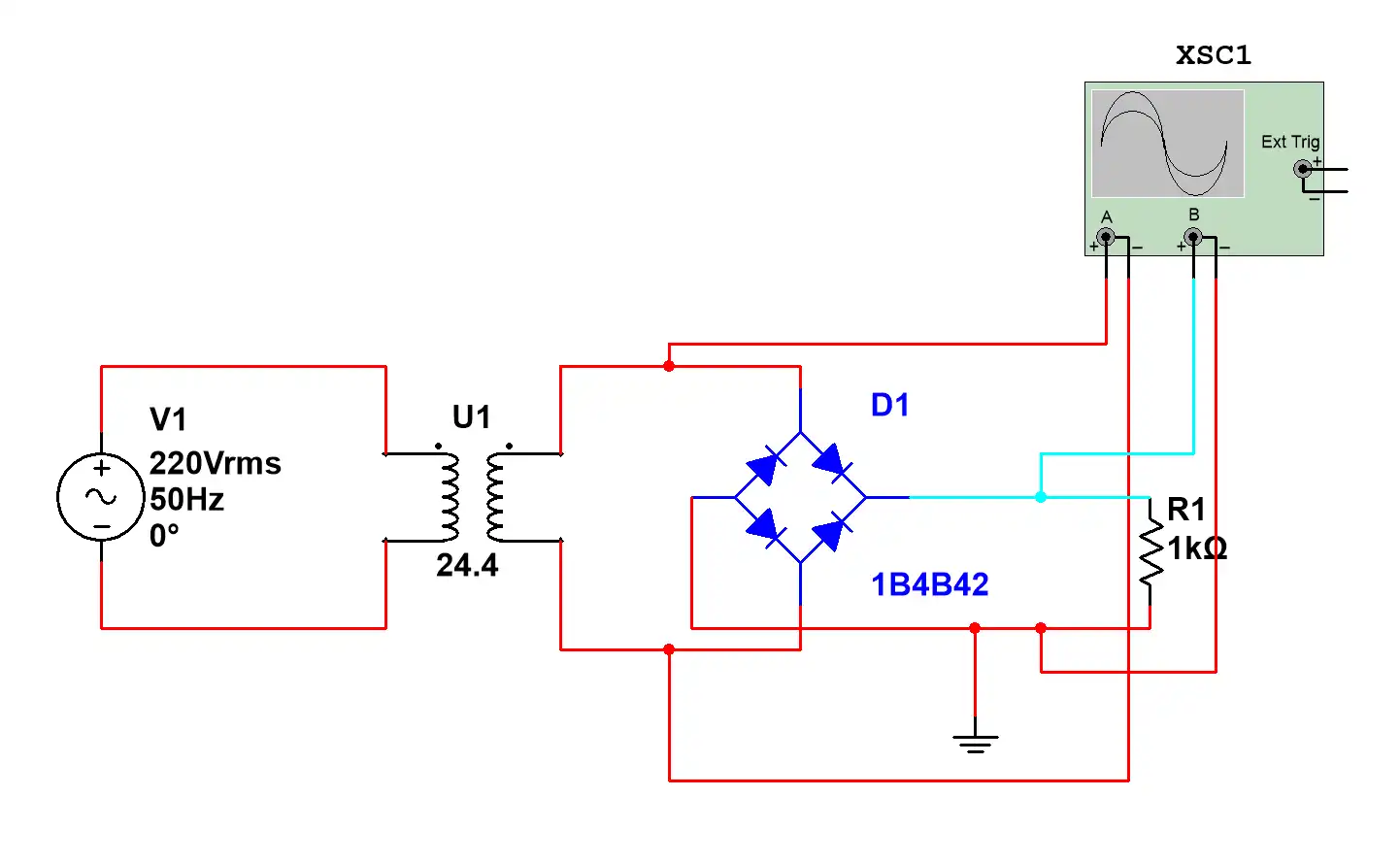 Fig 3. Simulation Circuit - Multisim
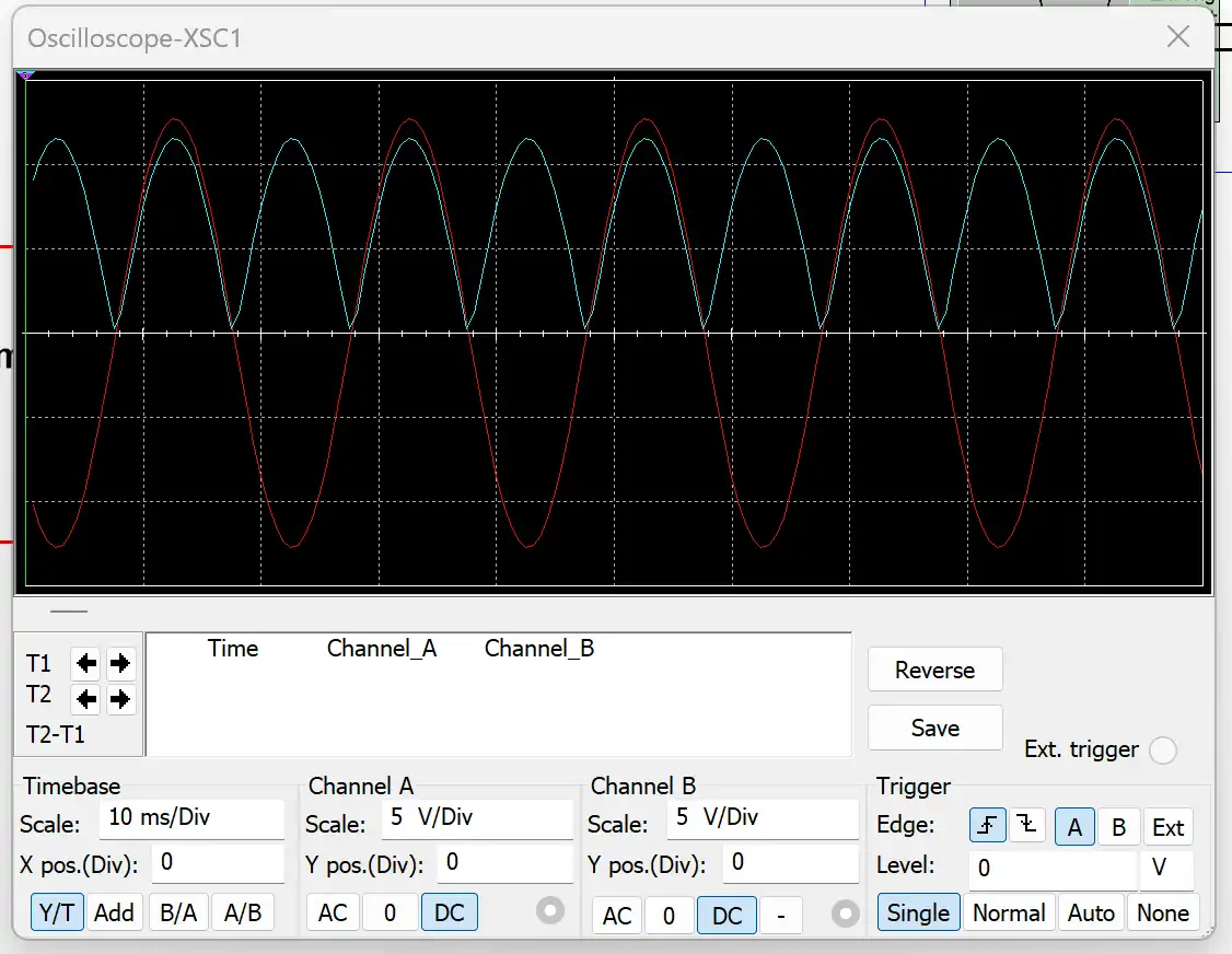 Fig 4. Simulation Graph - Multisim
PCB Design
Altium Designer
To design a PCB in Altium, you can follow these steps:
Create a Project
To start a new design, go to File > New > Project. Name your project and save it.
Schematic and PCB File
In the project, click with the right mouse button and select "Add New to Project" you can add a Schematic and PCB. This will create a new schematic and PCB file where you can design your circuit.
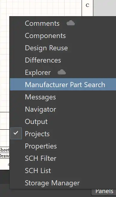
Manufacturer Part Search
To find the components you need, you can use the Manufacturer Part Search extension. Its in the Panels menu at the bottom right corner.
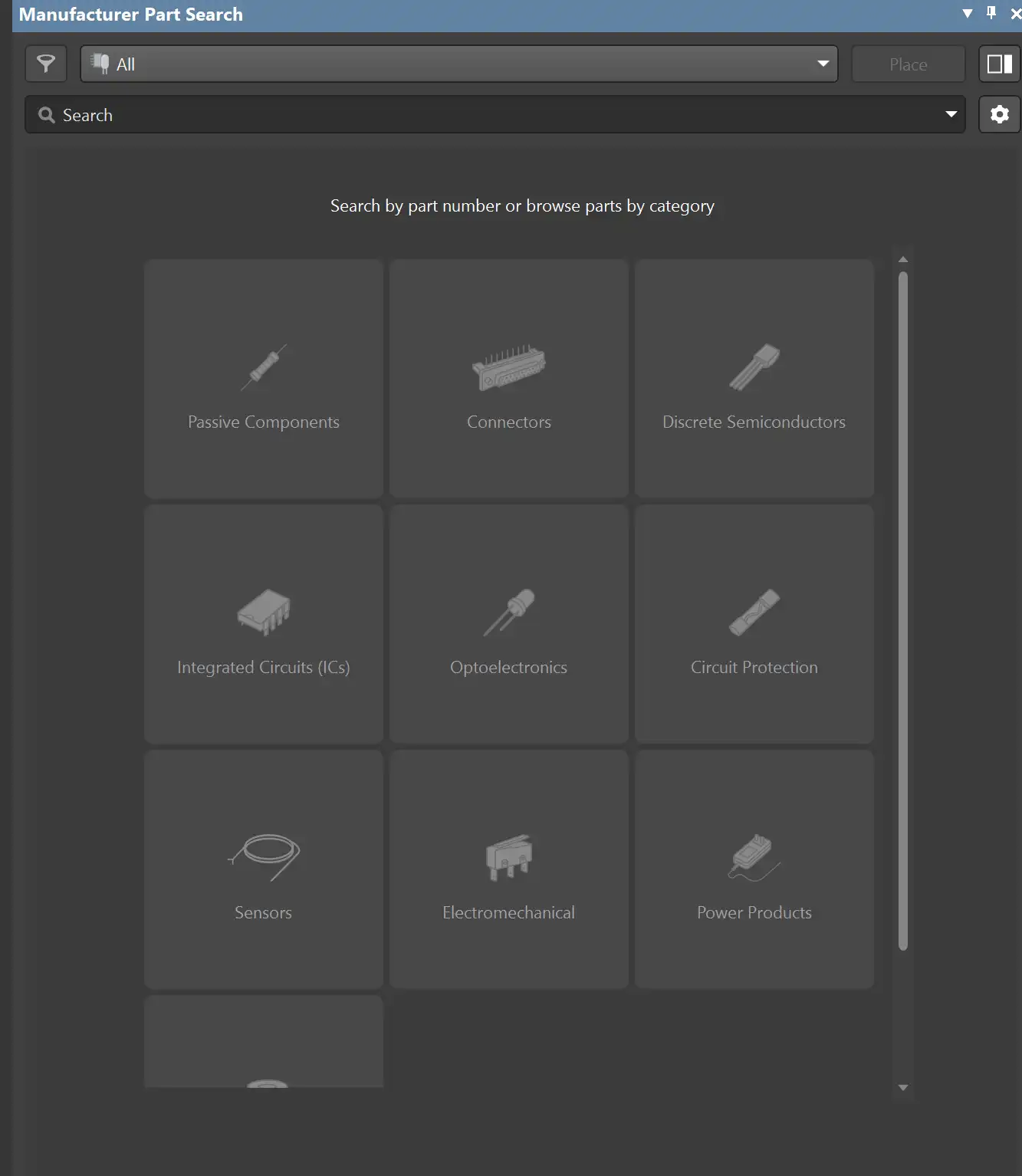
Components
This tool allows you to search for components from different manufacturers. You can find a wide range of categories and filter your search based on different parameters.
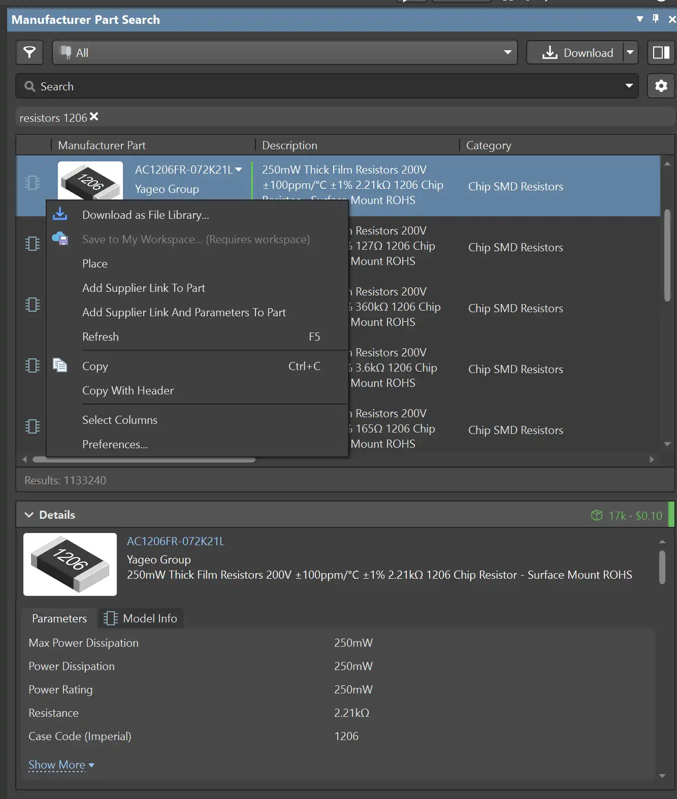
Place
Once you find the component you need, you can place the footprint in your schematic by clicking the right button and then "Place". This will add the component to your schematic and you can connect it to other components to create your circuit. Before placing the component, you can also check its properties to make sure it has the correct specifications for your design.
Toolbar
In the top toolbar, you cand find different tools to connect your components, add wires, and create buses. You can also find tools to add text and labels to your schematic to make it more organized and easier to understand.
Power port
You can find different types of power ports in this menu to add to your schematic.
Net Label
To make your schematic more organized, you can use net labels, instead of wires, to name the different connections in your circuit. This will help you identify different nodes and make it easier to understand the circuit.
Circuit
Ensured all the components you used had footprints apropriate for you to solder them later. The recommended sizes are 0805 and 1206 for SMD Components.
Annotation
Before change to the PCB File, you need to annotate your schematic. This process assigns a unique identifier to each component in your circuit. To annotate, go to Tools > Annotation > Annotate Schematics Quietly.
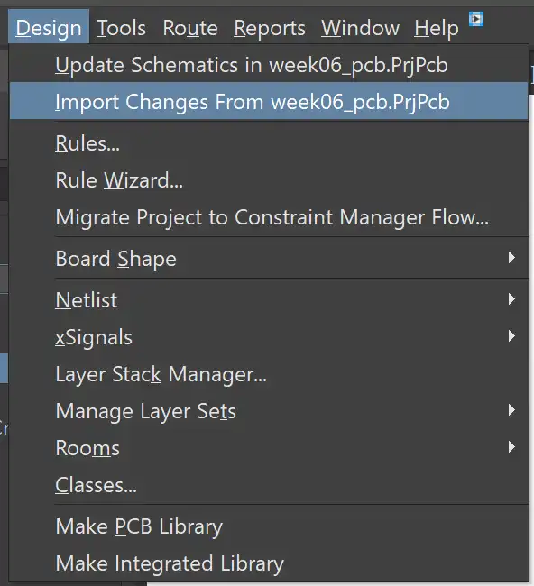
PCB File
Once your schematic is ready, you can change to the PCB file. To place the components in the PCB workspace, go to Design > Import Changes from [Your Schematic File Name]. This will open a new window where you can select the components you want to place in the PCB layout. Once you have selected the components, click on "Execute Changes" and they will be placed in the PCB workspace.
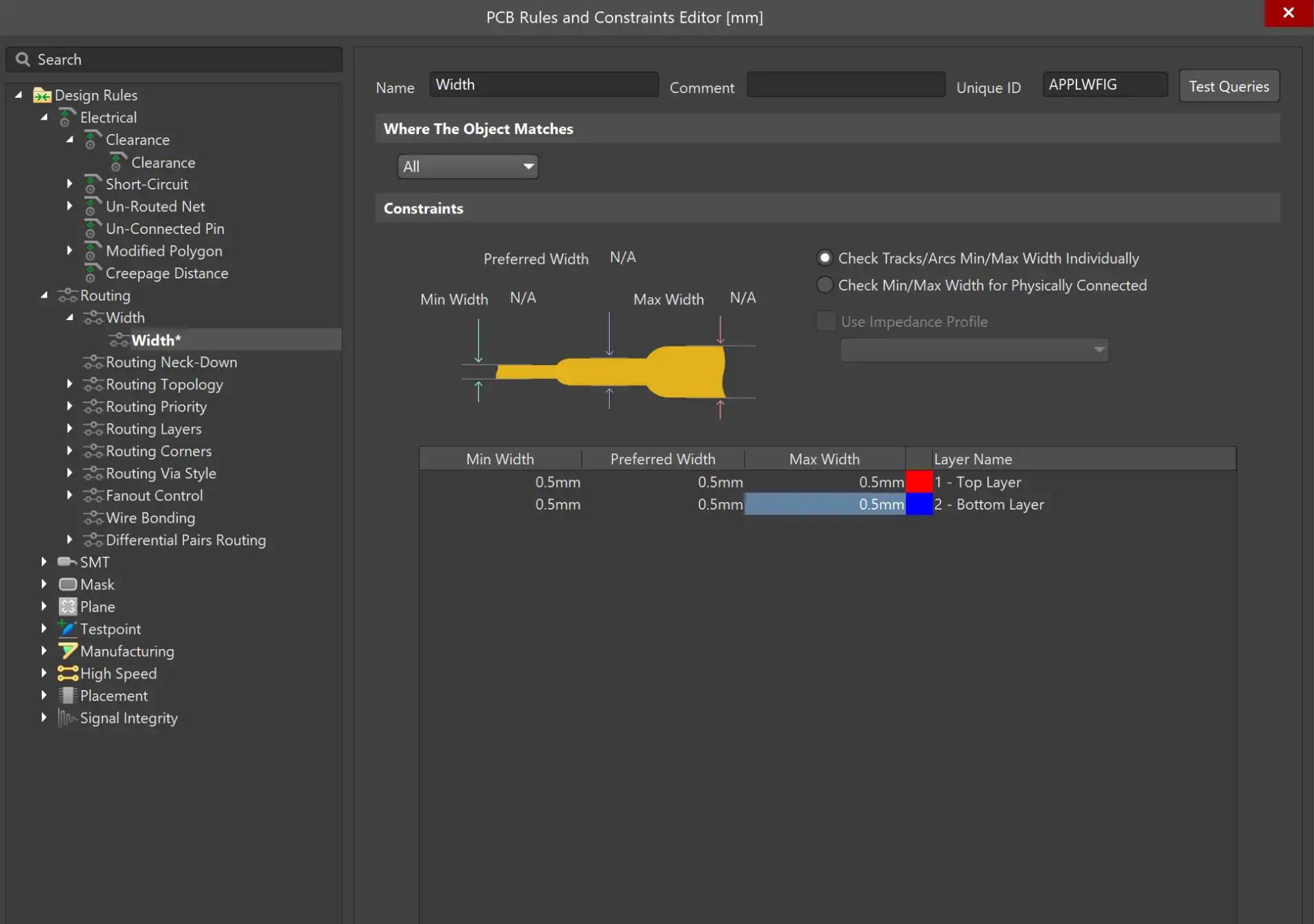
Rules
Before organizing the components in your PCB layout, you need to set up the design rules. This process ensures that your PCB design meets the manufacturing requirements and prevents any issues during the fabrication process. To set up the design rules, go to Design > Rules. Here you can adjust different parameters such as trace width and clearance.
- Width: 0.5 mm
- Clearance: 0.4 mm
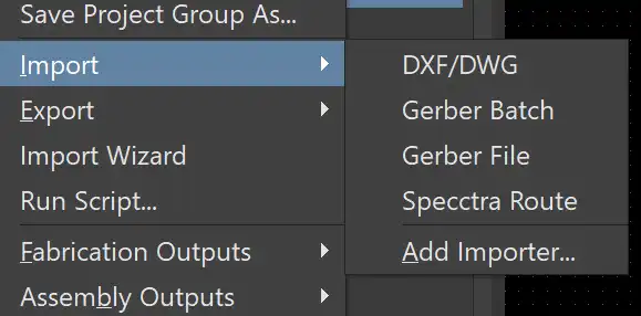
Import DXF
To personalize the board outline, you can vectorize the design you want and save it as a DXF file. Then go to File > Import > DXF/DWG.
If the DXF File option doesn't appear, you need to go to "Add Importer" and enable the DXF Importer extension.
Import
Make sure to select the correct units and scale of your original vector file. After importing, you can adjust the track width by double-clicking on the the lines.
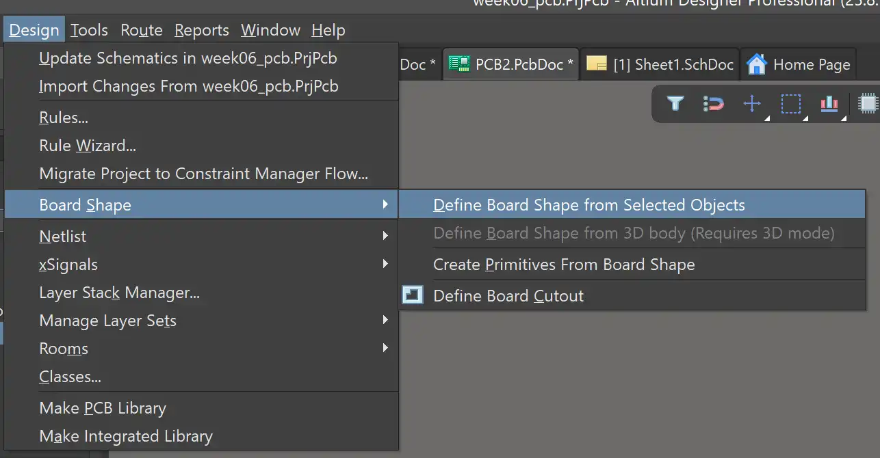
Define Board Shape
To define the board shape, you need to select all the lines of the imported DXF file and then Design > Board Shape > Define Board Shape from Selected Objects. This will set the outline of your PCB based on the imported design.
❮
❯
Add Libraries
If a footprint for a specific component is not available in the Altium library, you can download it from Snap Magic.
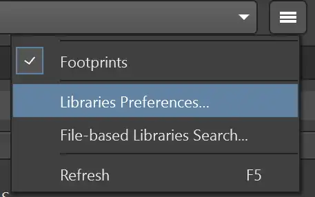
Download the footprint you need, here is where a find the Xiao Footprint i used in my PCB. Go to the Components panel, click the three lines and select "Libraries Preferences"
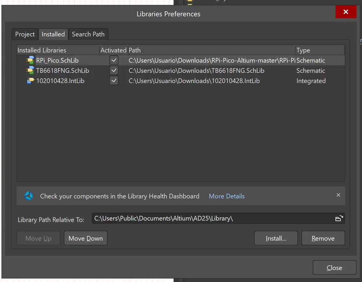
Go to the Installed tab and install the file downloaded.
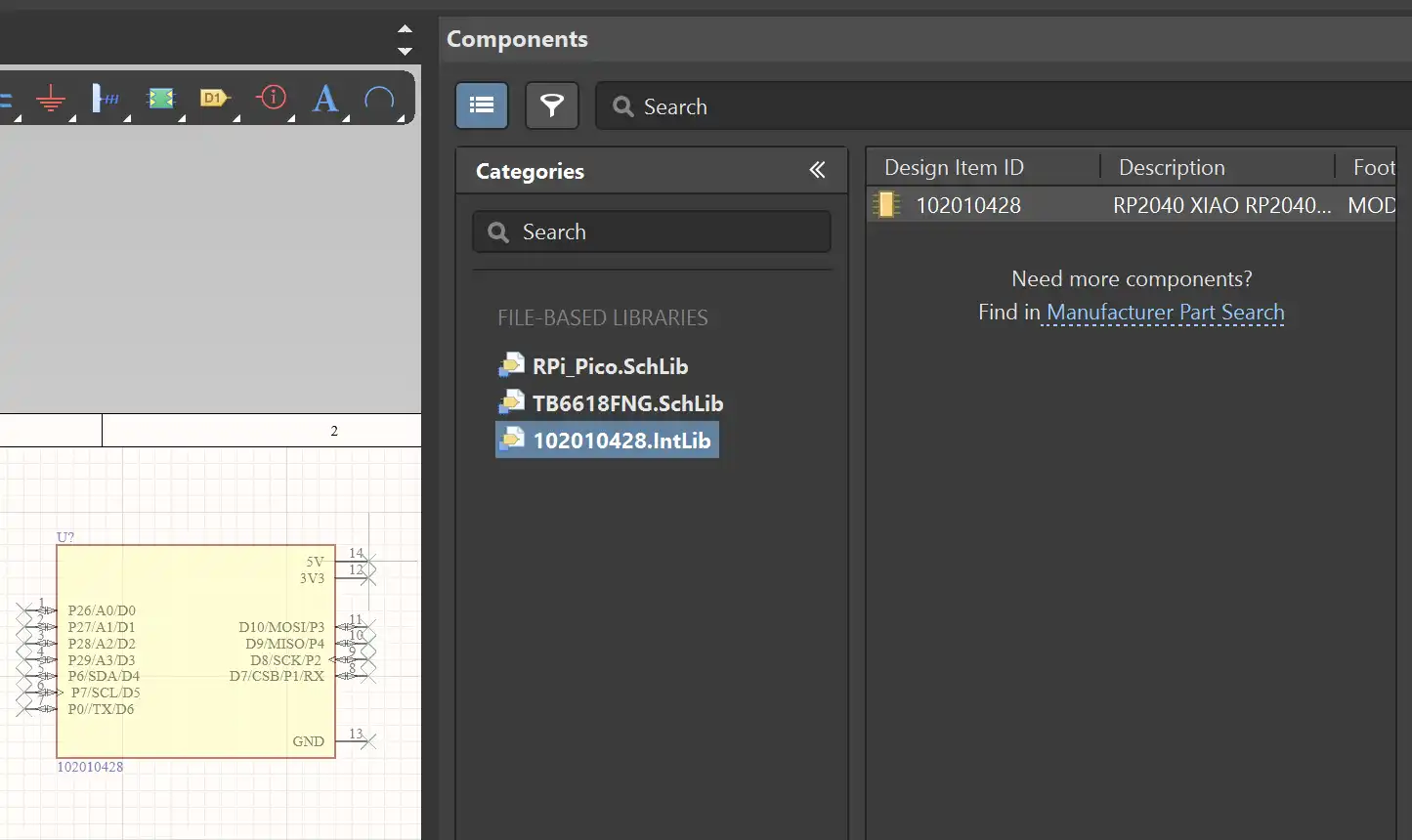
Now the footprint will appear in the Components panel and you can add it by double-clicking in the library.
Results
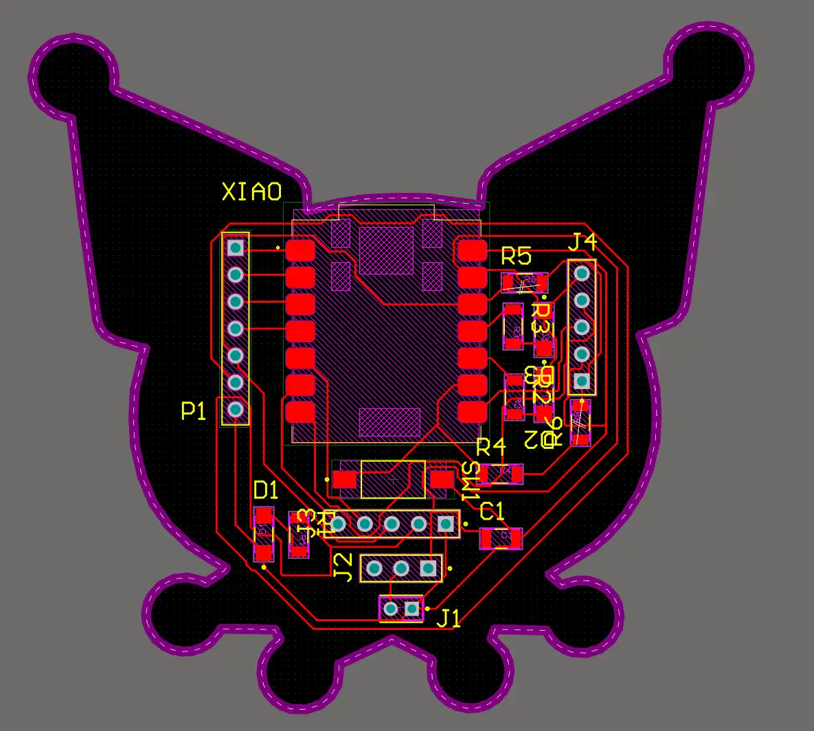 Fig 5. PCB 2D - Altium
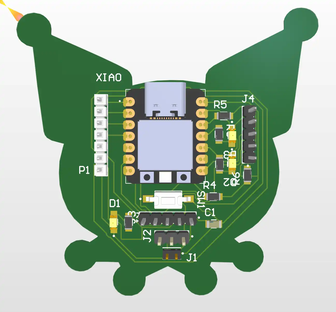 Fig 6. PCB 3D - Altium
Files
You can download the files created and used during this week here:
📄 Files.zip