This week's goal is to design a Printed Circuit Board (PCB) from scratch using an Electronic Design Automation (EDA) software. I will build the first brain of my Smart Goal project, adding a XIAO RP2040, a button, an LED, and expansion pins for an OLED screen.
For this mission, I chose KiCad because it is open-source, powerful, and strictly logical.
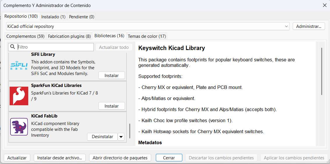
To ensure my digital design matches the real components we have in the Fab Lab inventory, the first critical step was installing the official Fab Academy Library in KiCad.
Adding the Fab footprint and symbol libraries in KiCad's Plugin and Content Manager.
03. THE BLUEPRINT (SCHEMATIC DESIGN)
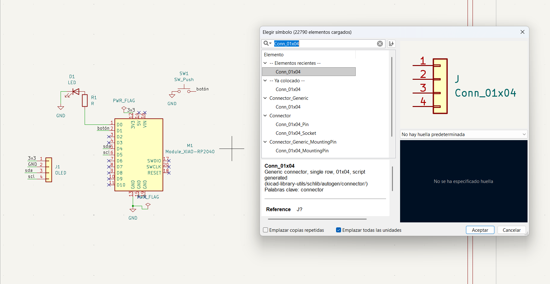
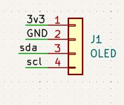
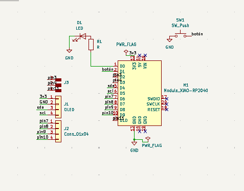
I started placing my components in the schematic editor. I added the Seeed Studio XIAO RP2040 as the main brain, a 1206 LED, a tactile button, and headers for the future OLED screen.
01. Placing components.
02. Connecting pins.
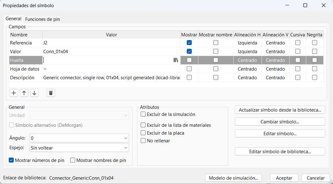
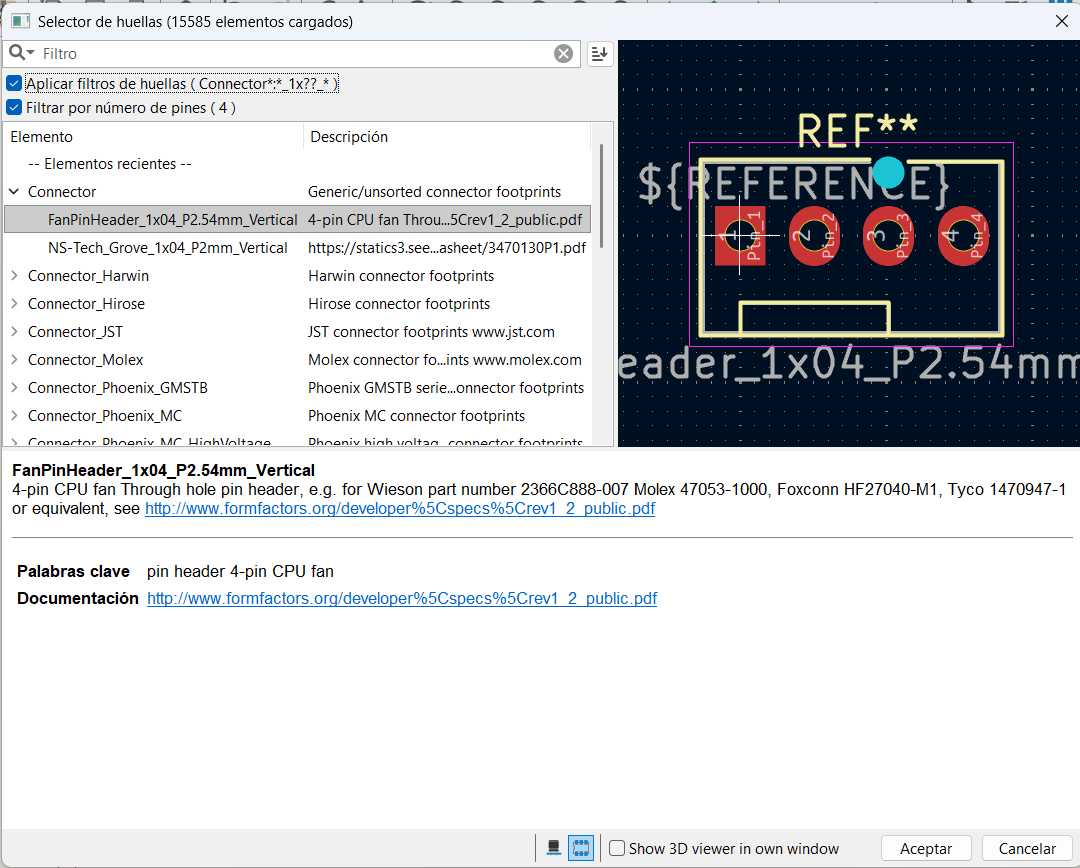
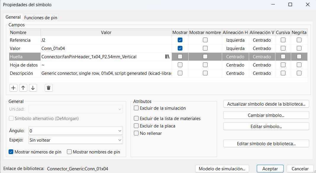
ASSIGNING FOOTPRINTS
1 / 4
01. Opening the footprint assignment tool.
02. Selecting the official Fab library.
03. Choosing the 1206 SMD sizes for LEDs and Resistors.
04. Footprints assigned successfully!
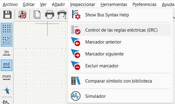
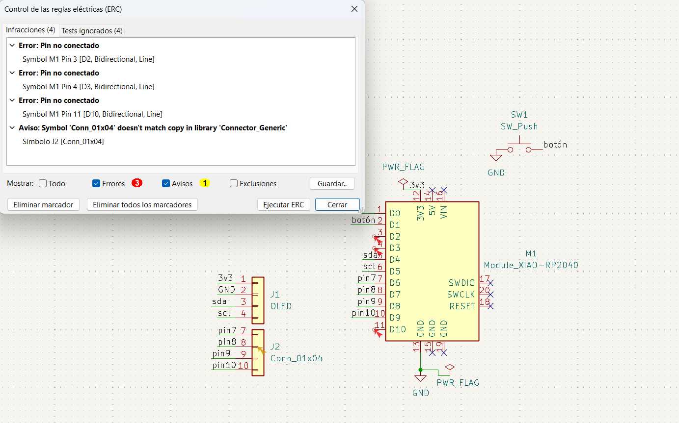
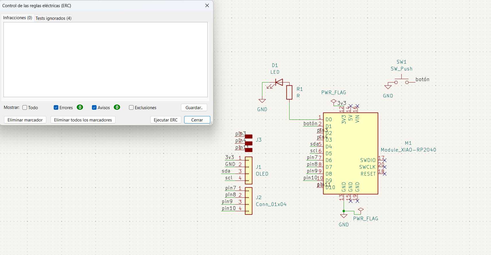
ERC CHECK
1 / 4
01. Running the Electrical Rules Checker.
02. Adding a PWR_FLAG to solve power input warnings.
03. Zero fatal errors. Logic is solid!
04. The completed and verified schematic diagram.
COMPONENT LOGIC & CALCULATIONS
Before wiring the schematic, I needed to define the specific values for my components to ensure the circuit works safely. The brain of the board is the XIAO RP2040, which operates at a 3.3V logic level. For visual feedback, I am using a standard 1206 SMD LED.
LED Resistor Calculation:
To prevent the LED from burning out, I needed to calculate the correct current-limiting resistor using Ohm's Law (R = V / I).
Source Voltage (Vs): 3.3V (Output from the XIAO RP2040)
LED Forward Voltage (Vf): ~2.0V (Standard for a Red/Green LED)
Desired Current (I): 10mA (0.01A) for a bright but safe light
R = (3.3V - 2.0V) / 0.01A = 130 Ohms
Since 130 Ohms is the absolute minimum required, I chose a standard 330 Ohm resistor from the Fab Lab inventory. This slightly higher value keeps the LED perfectly visible while saving power and ensuring a long lifespan for the component.
05. THE SECRET IDENTITY (INKSCAPE TO KICAD)
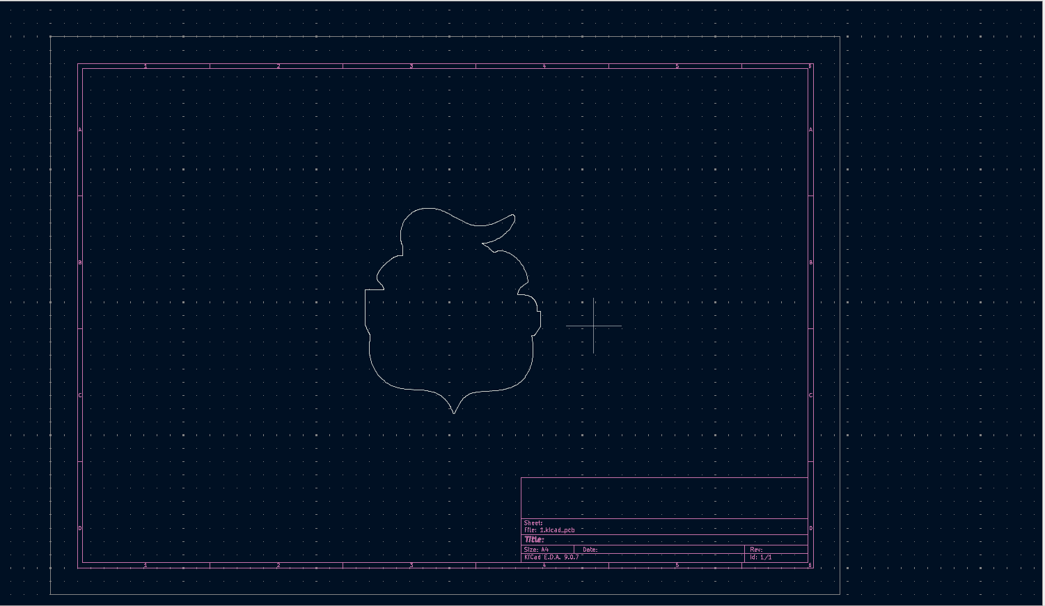
I wanted the PCB to have the shape of the Puebla soccer team shield! Importing a complex SVG directly into KiCad's Edge.Cuts layer often causes double-line errors. I used Inkscape to clean it up.
This was the original logo reference for my board's shape.
1 / 6
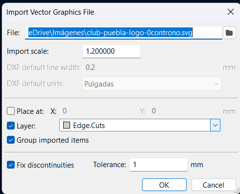
01. To import the board shape into the PCB editor, I selected "import" and "graphics".
02. Then I selected the file as SVG, I needed to change the layer to Edge.Cuts.
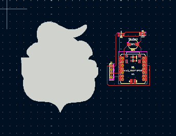
03. This is how appears when I imported the SVG.
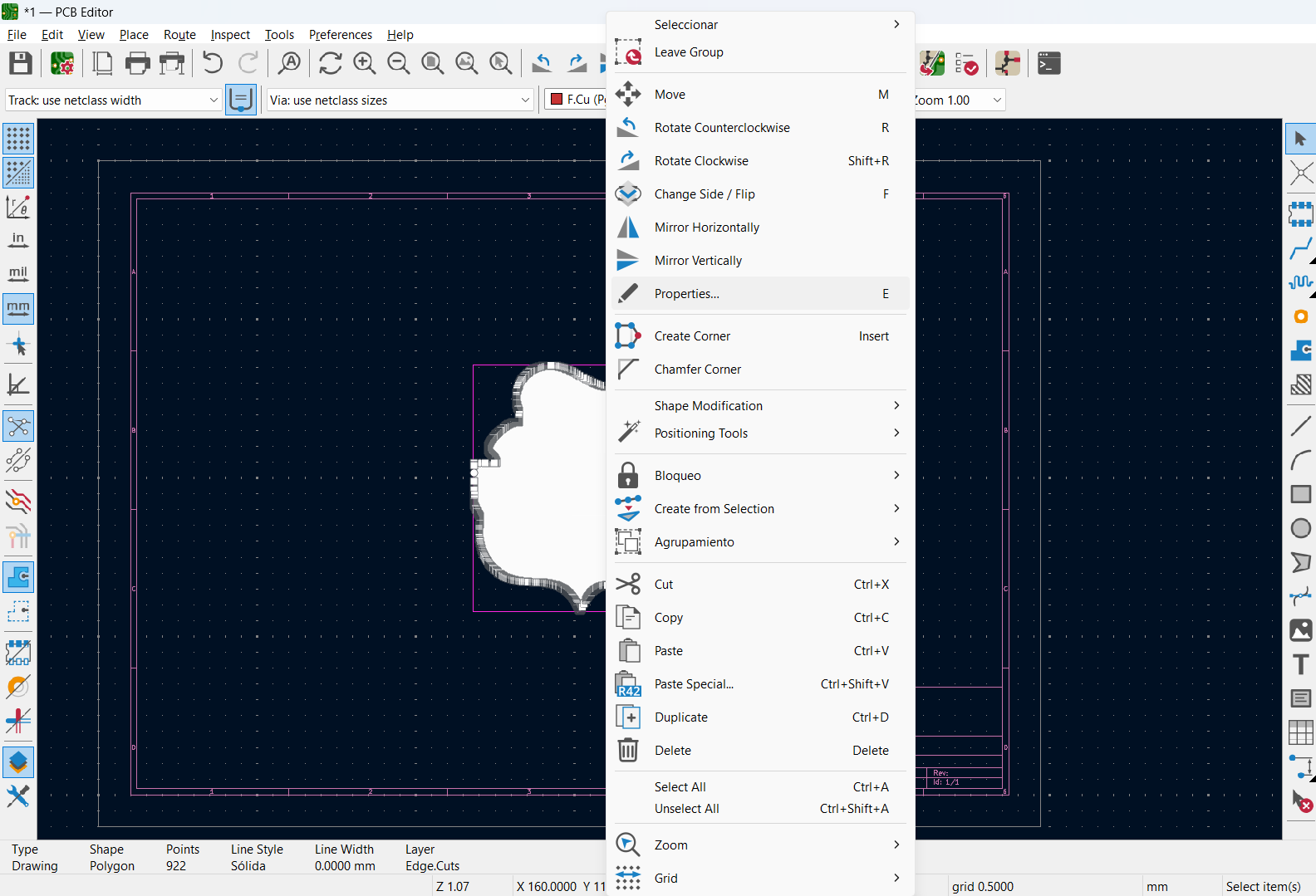
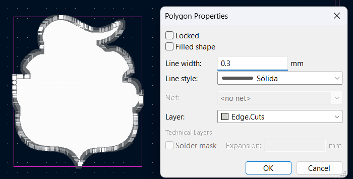
04. To looks like a single path, I had to remove the fill, all we need is clicking twice on the object and select "properties".
05. Imported to Edge.Cuts! I had to uncheck "Filled shape" in KiCad and make sure to change the line width.
06. Now it looks like a single line and very clean.
now let´s go to import the schematic.
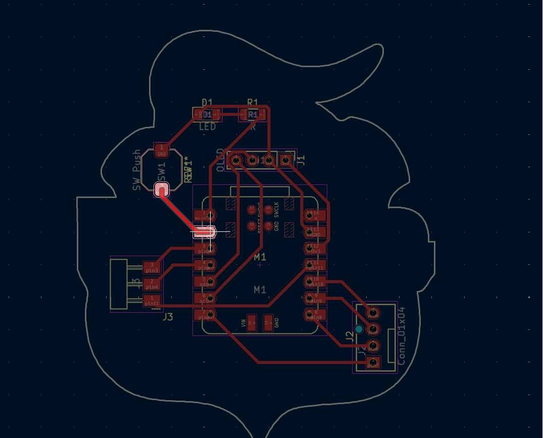
04. THE COPPER LABYRINTH (PCB LAYOUT)
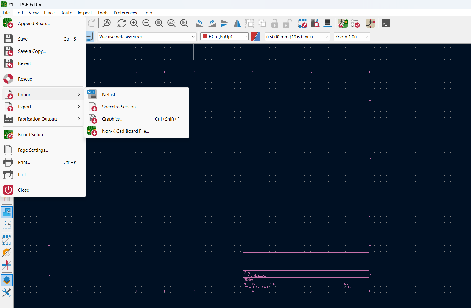
With the logic defined, I crossed the portal to the physical world by updating the PCB from the schematic (F8).
1 / 10
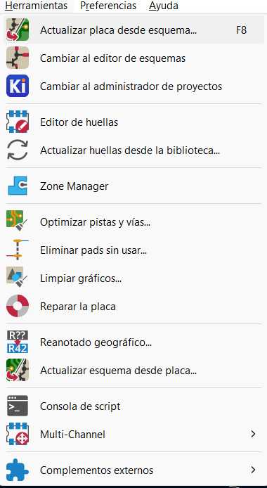
01. Tools > Update PCB from Schematic (F8).
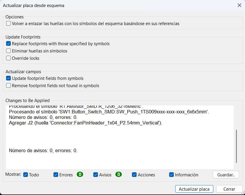
02. Reviewing the component changes to be imported.
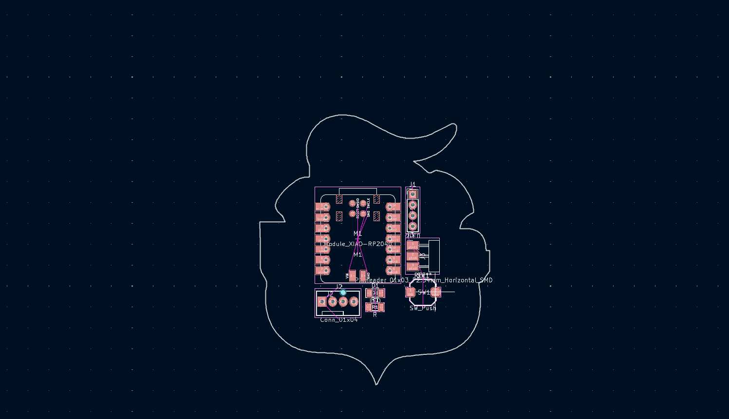
03. Dropping the components into the PCB editor.
04. The messy ratsnest before arrangement.
05. Setting the track width to 0.8mm safely around the board.
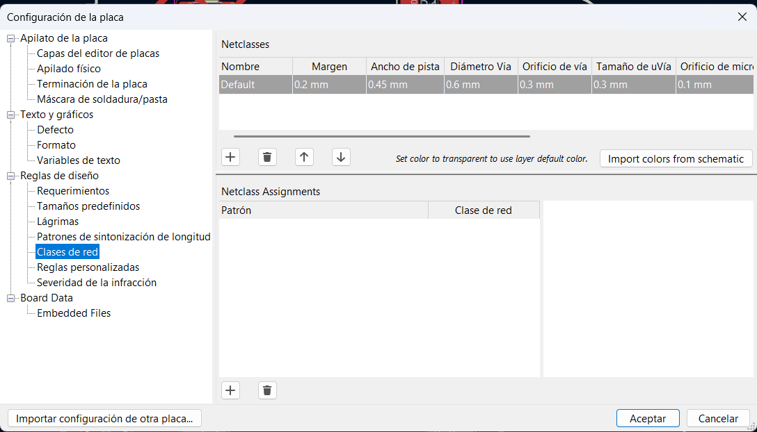
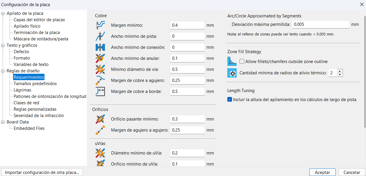
06. Setting the design rules, I´m making sure everything is with their proper spacing.
07. Routing the copper tracks avoiding crossings.
08. The final routed board, ready for its custom outline.
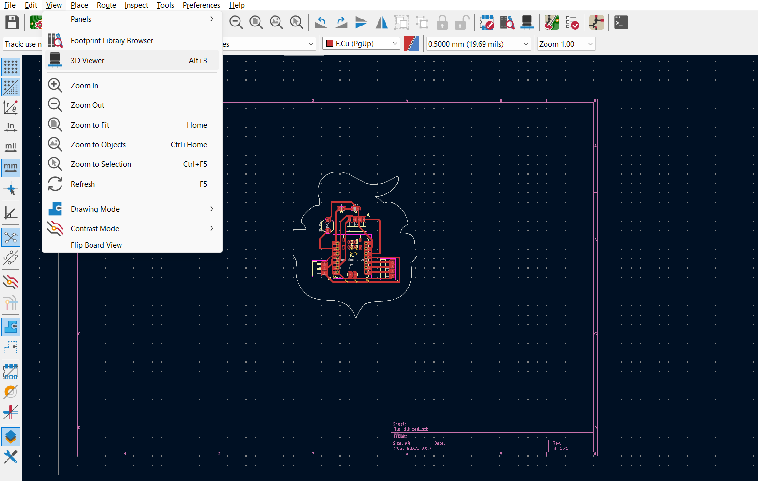
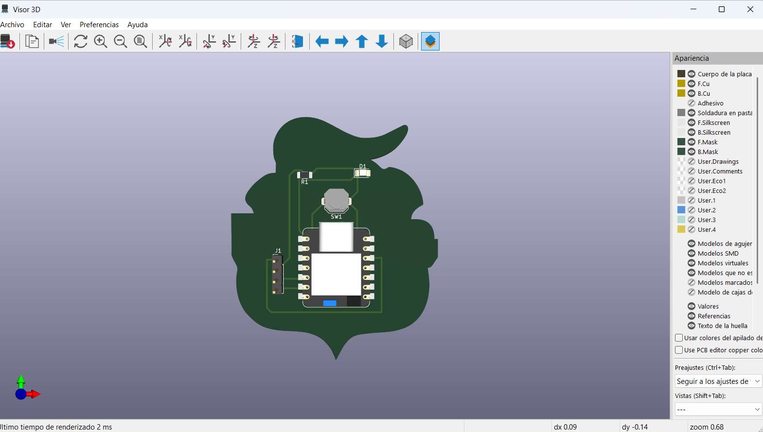
09. To preview the final 3D view of the PCB, all I need is to go to "view" and then to "3D Viewer".
10. The custom shape hugging the PCB components and the board shapeperfectly.
ESTABLISHING DESIGN RULES
Before routing a single track, I had to establish the Design Rules in KiCad's Board Setup. Since we are milling this board locally on a Roland SRM-20 instead of ordering it from a commercial factory, the physical size of our cutting tools dictates our digital rules.
Minimum Clearance (0.4 mm): This is the most critical constraint. The endmill used to isolate the copper traces is 1/64 inch (approximately 0.4 mm) wide. If the space between two traces is less than 0.4 mm, the machine's endmill physically cannot pass through, and the traces will remain connected, causing a short circuit.
Track Width (0.8 mm): Milling puts mechanical stress on the copper layer. While 0.4mm is the minimum, I set my default net class width to 0.8 mm. This guarantees highly robust paths that won't rip off the fiberglass board during cutting or when applying heat with the soldering iron.