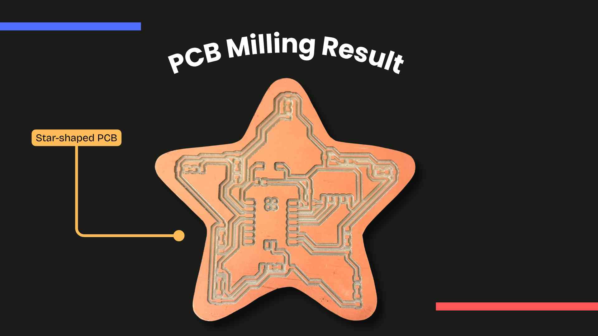
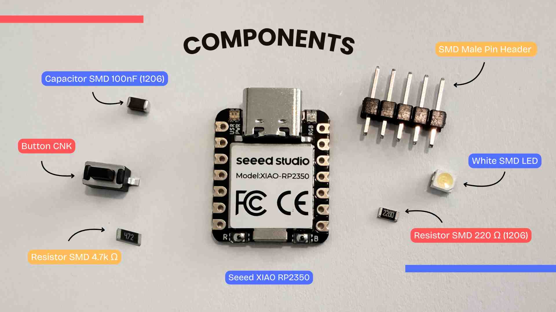
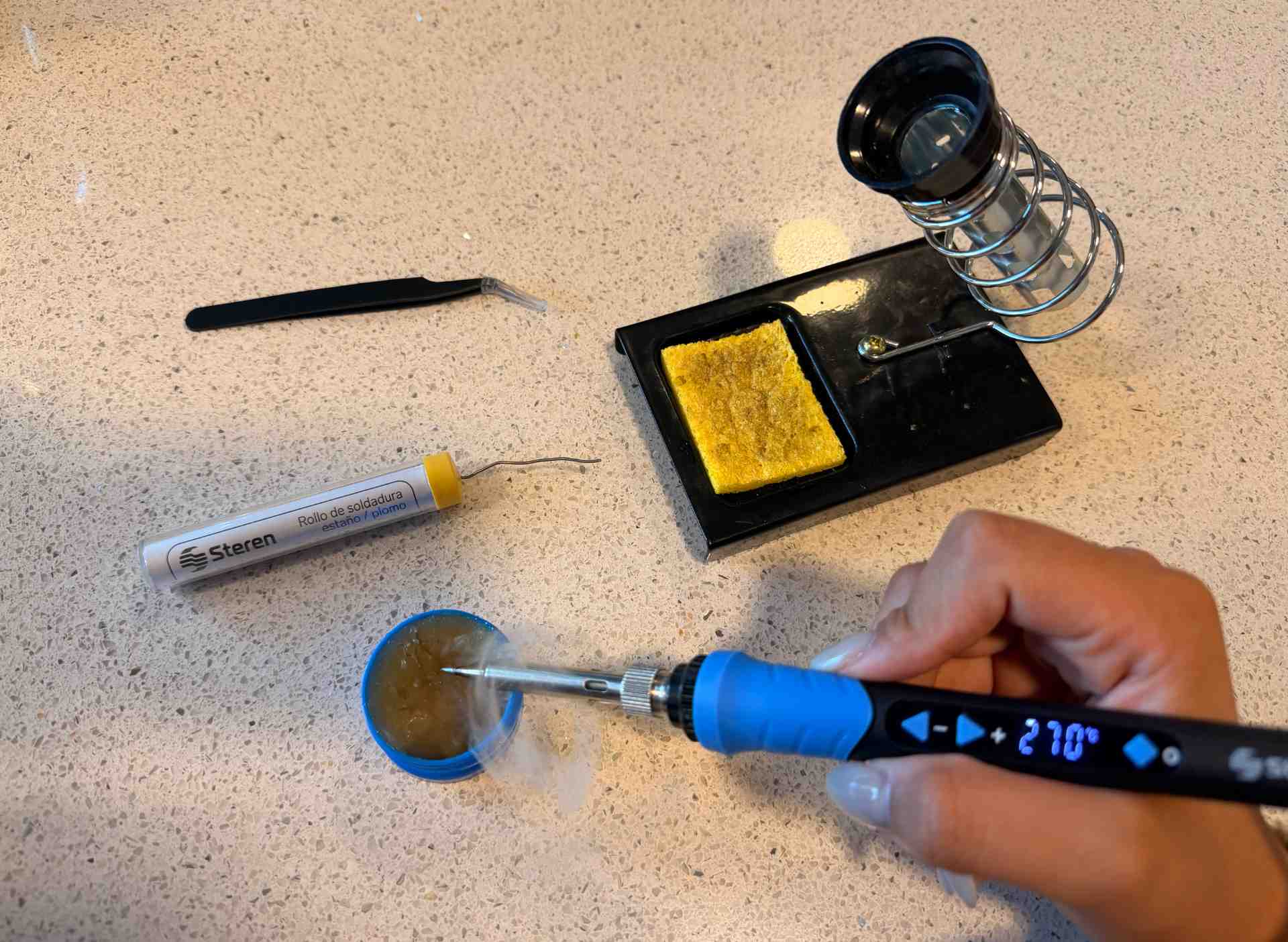
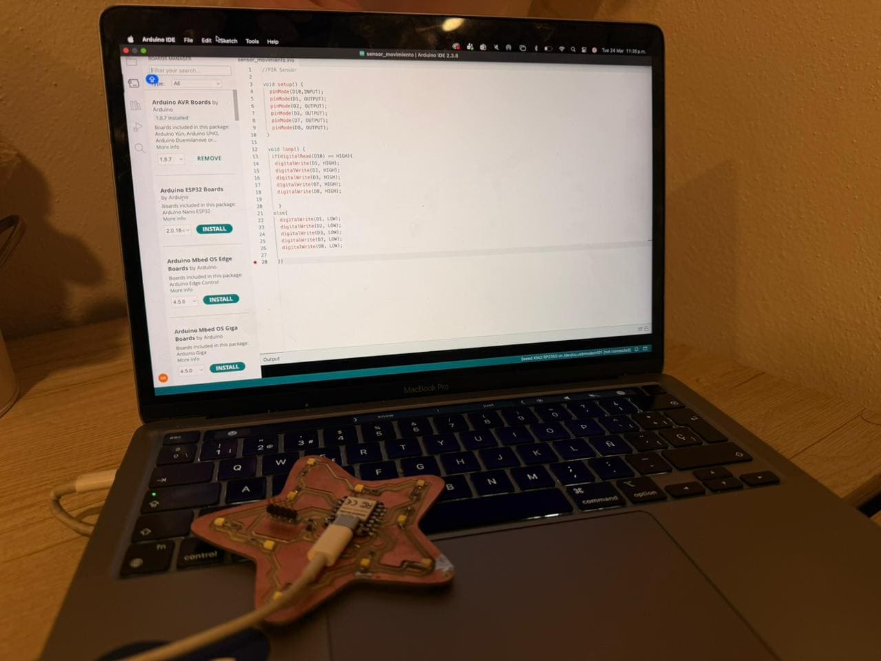
WEEK 8

TASK
MONDAY
WEDNESDAY
FRIDAY
MONDAY

✦ PCB Manufacturing

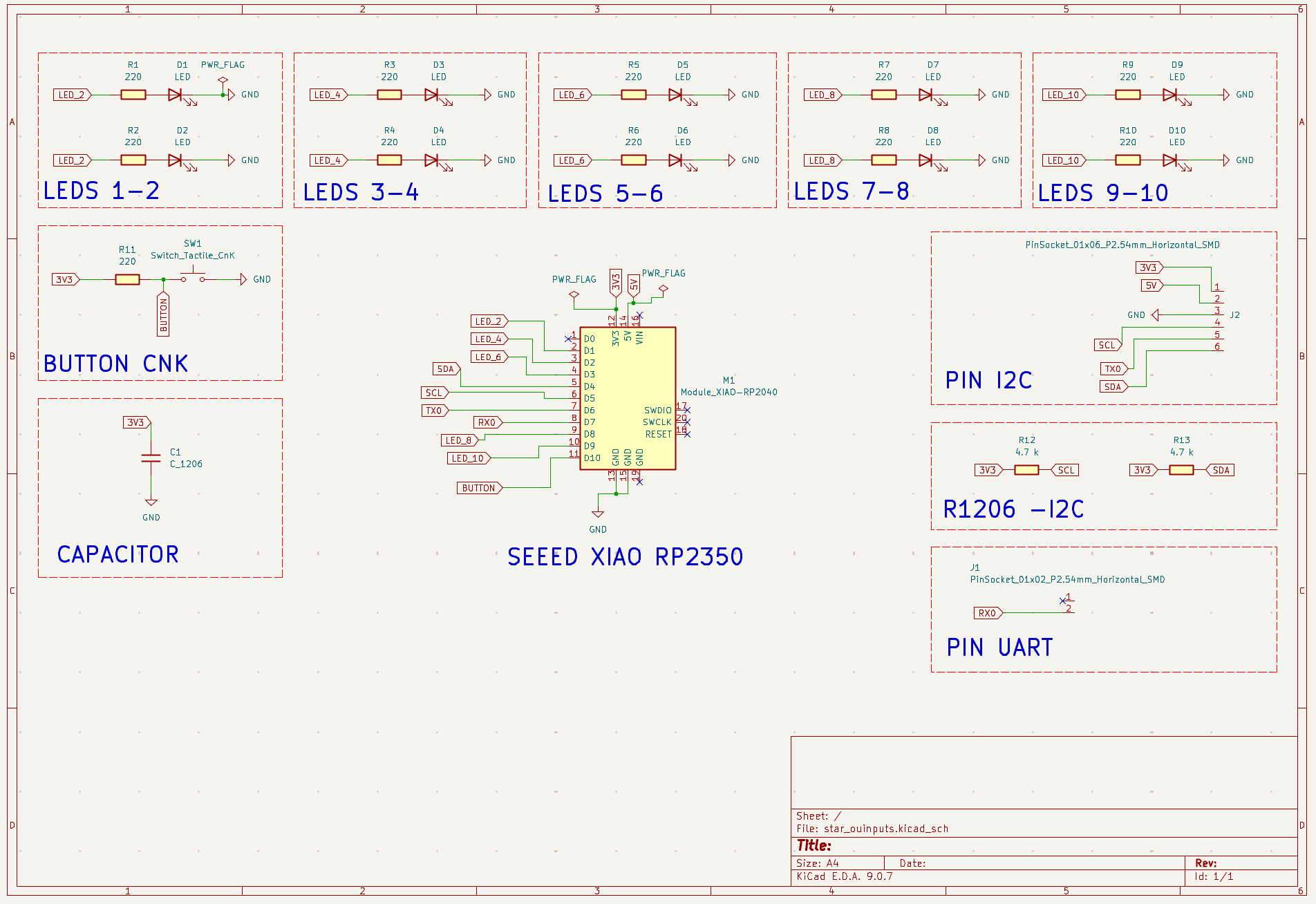
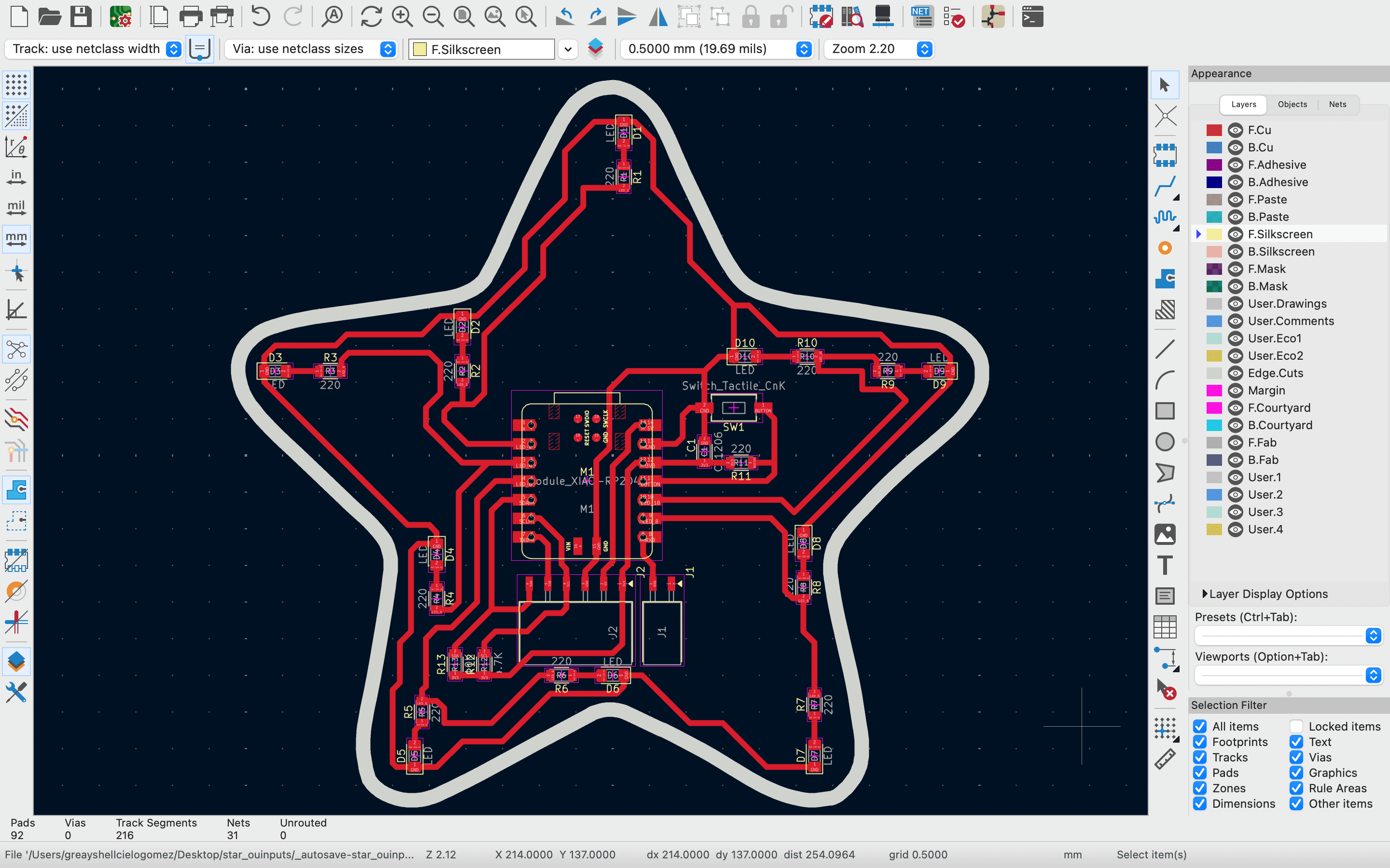
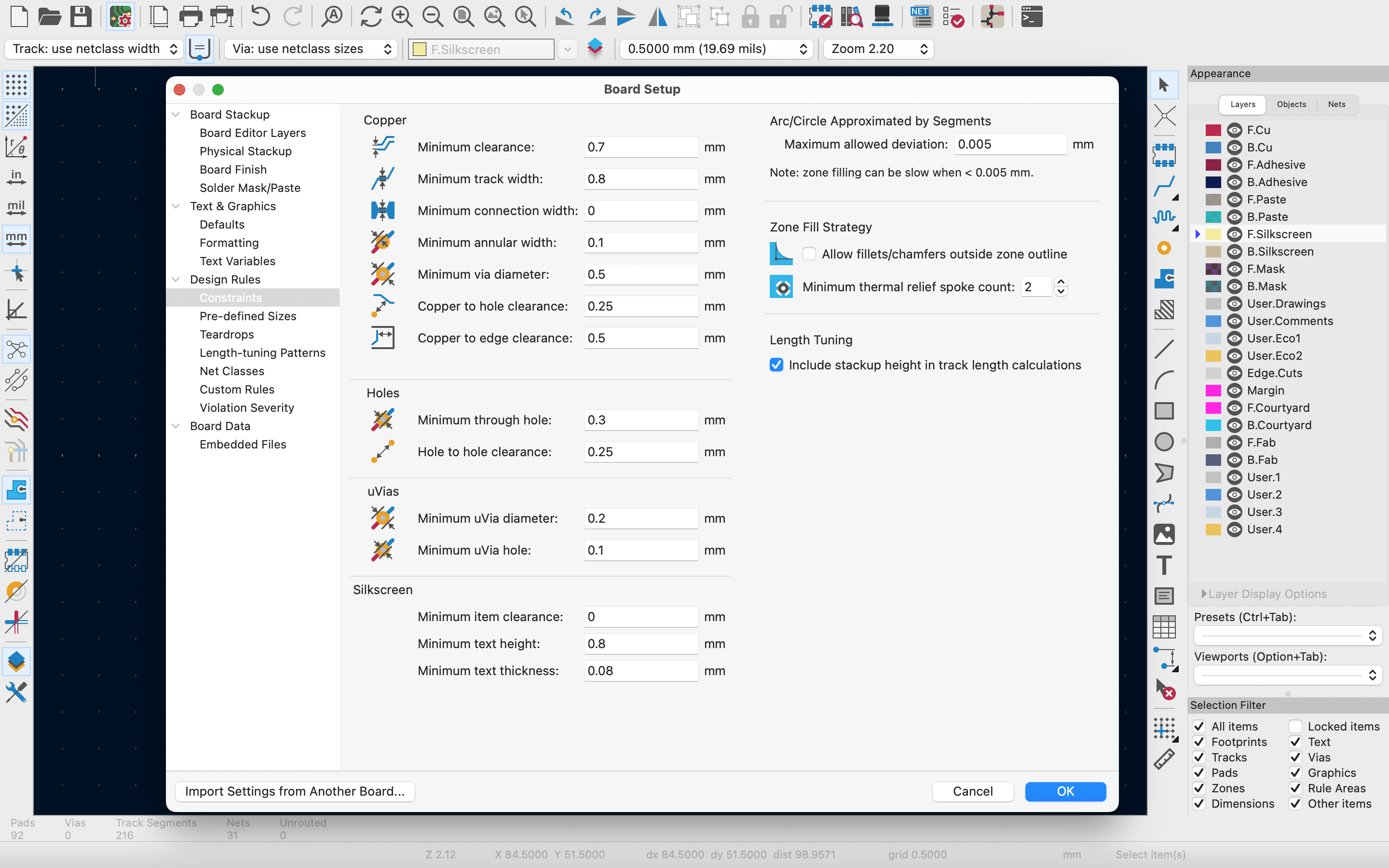
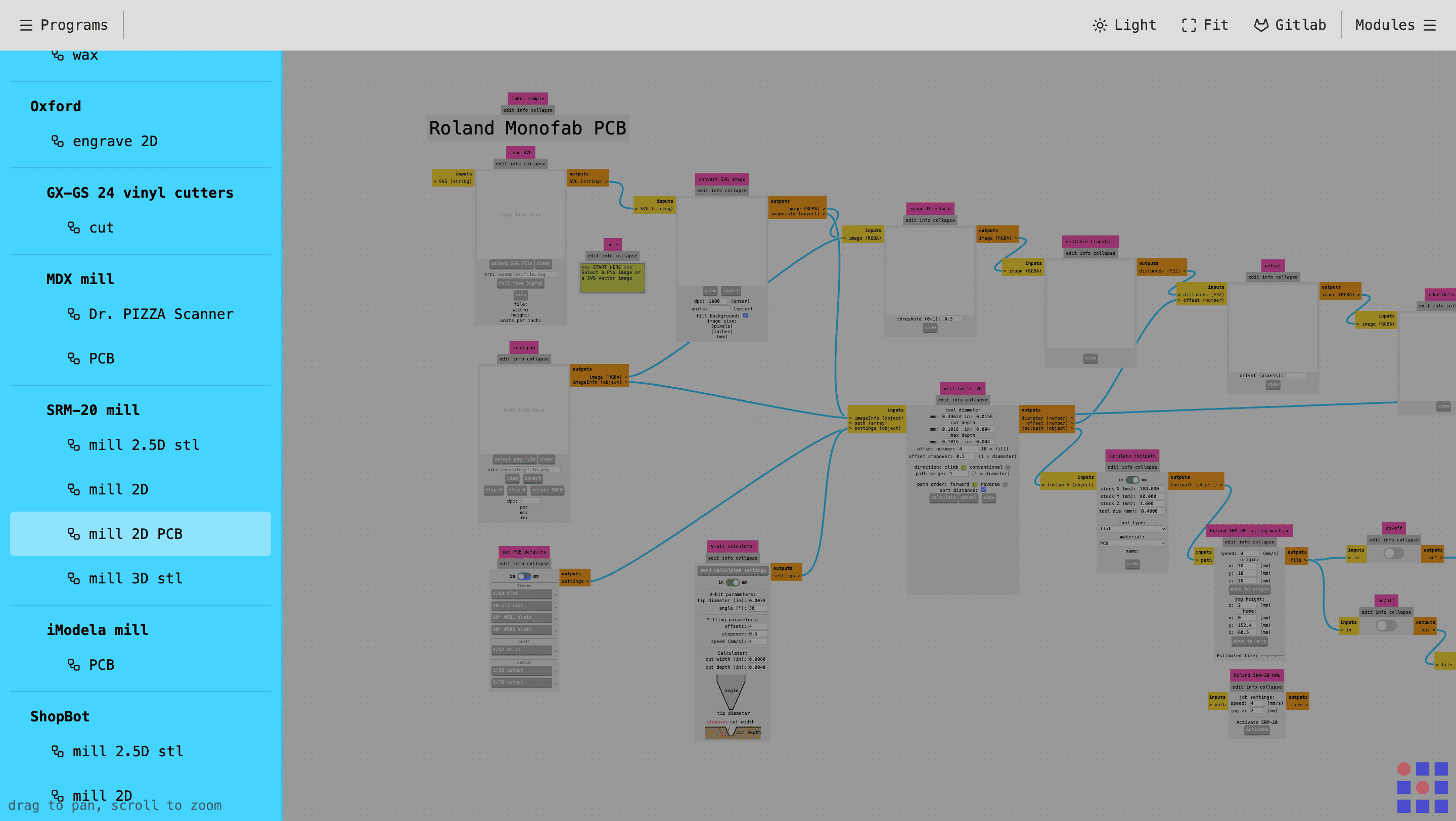
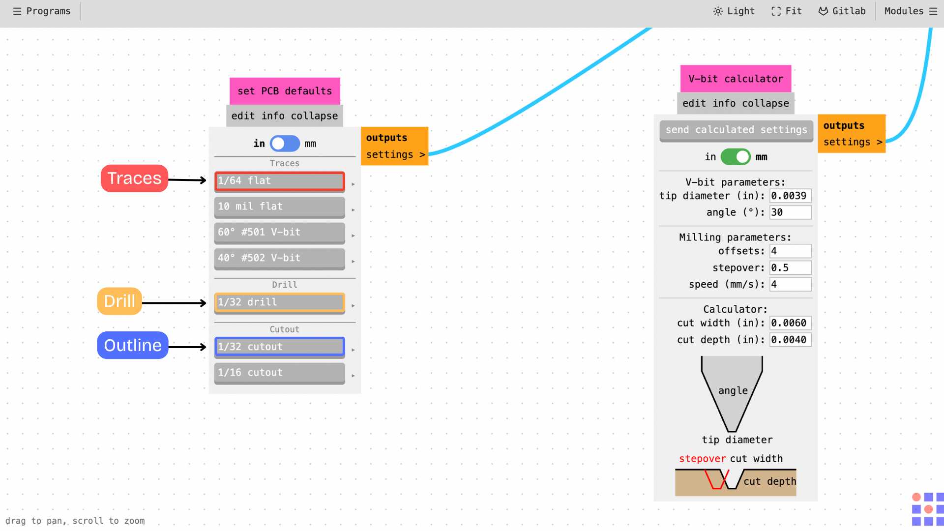
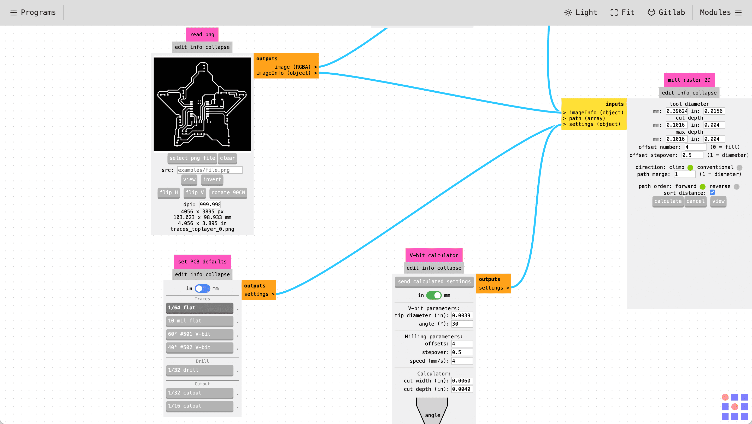
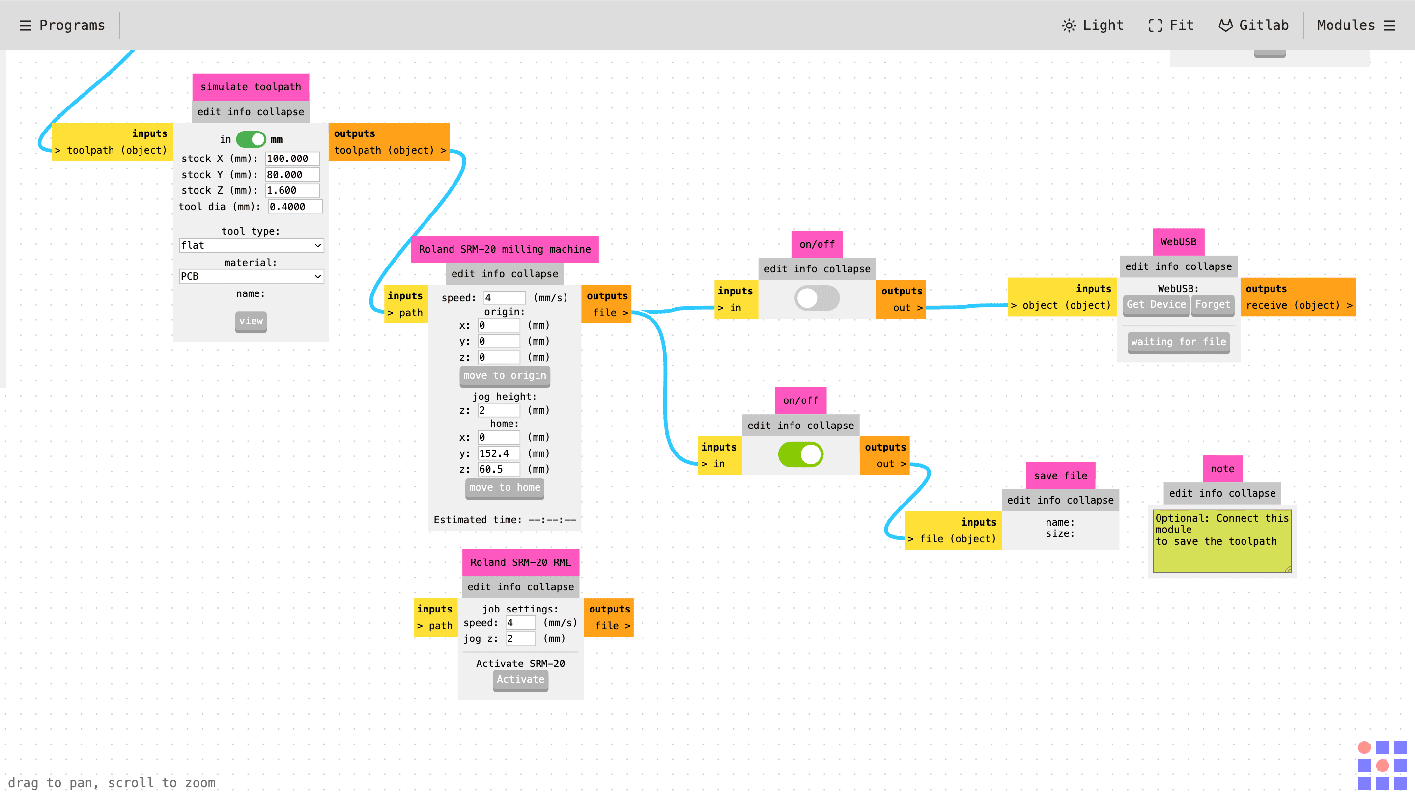
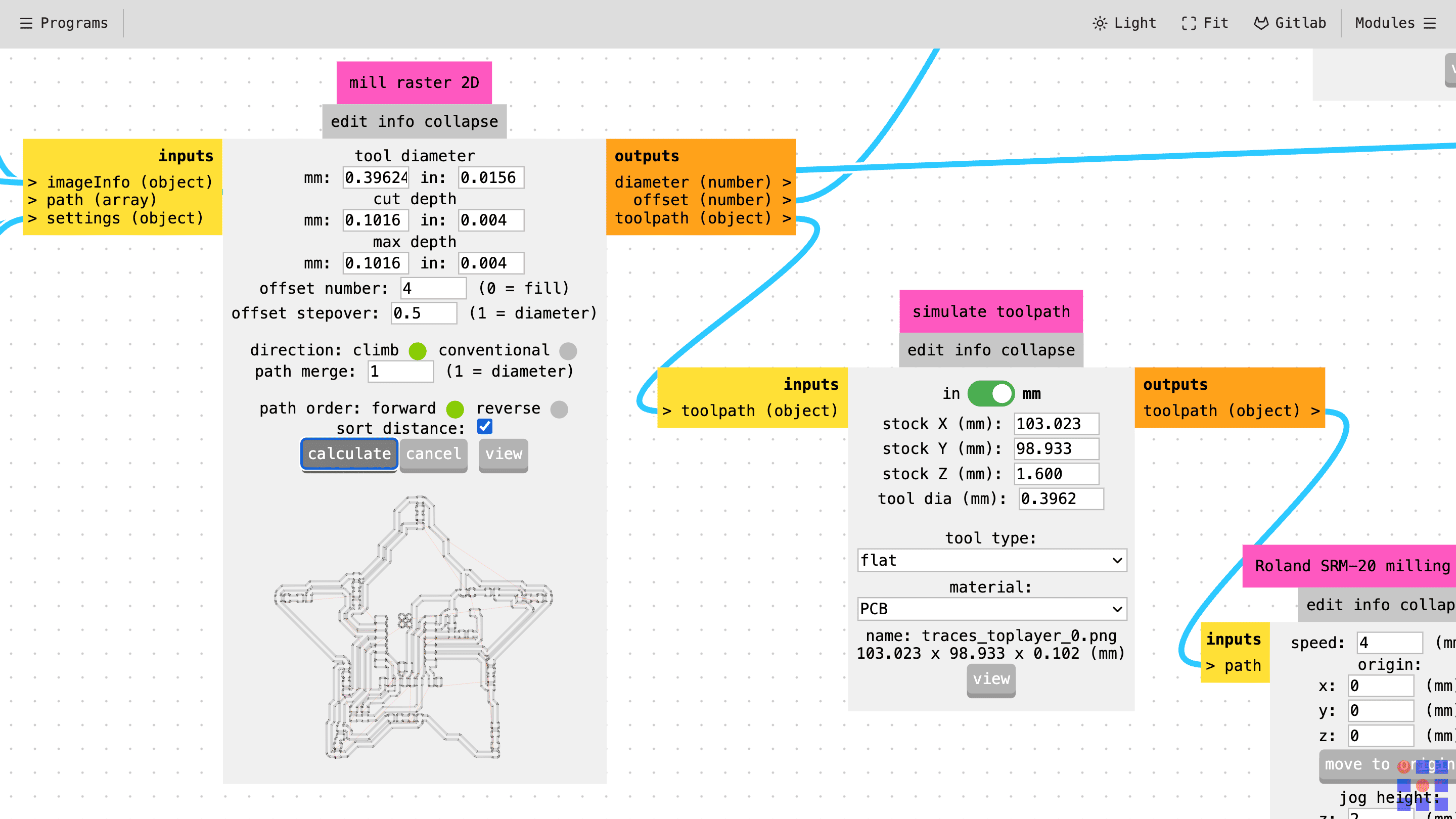
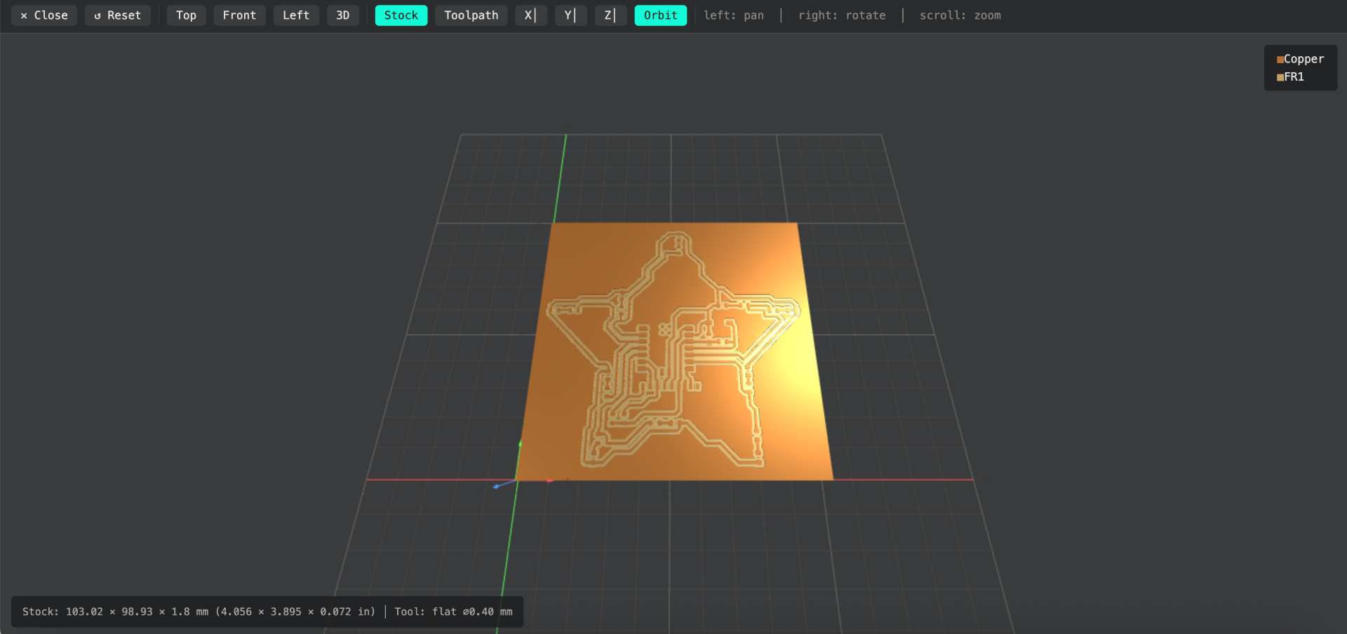
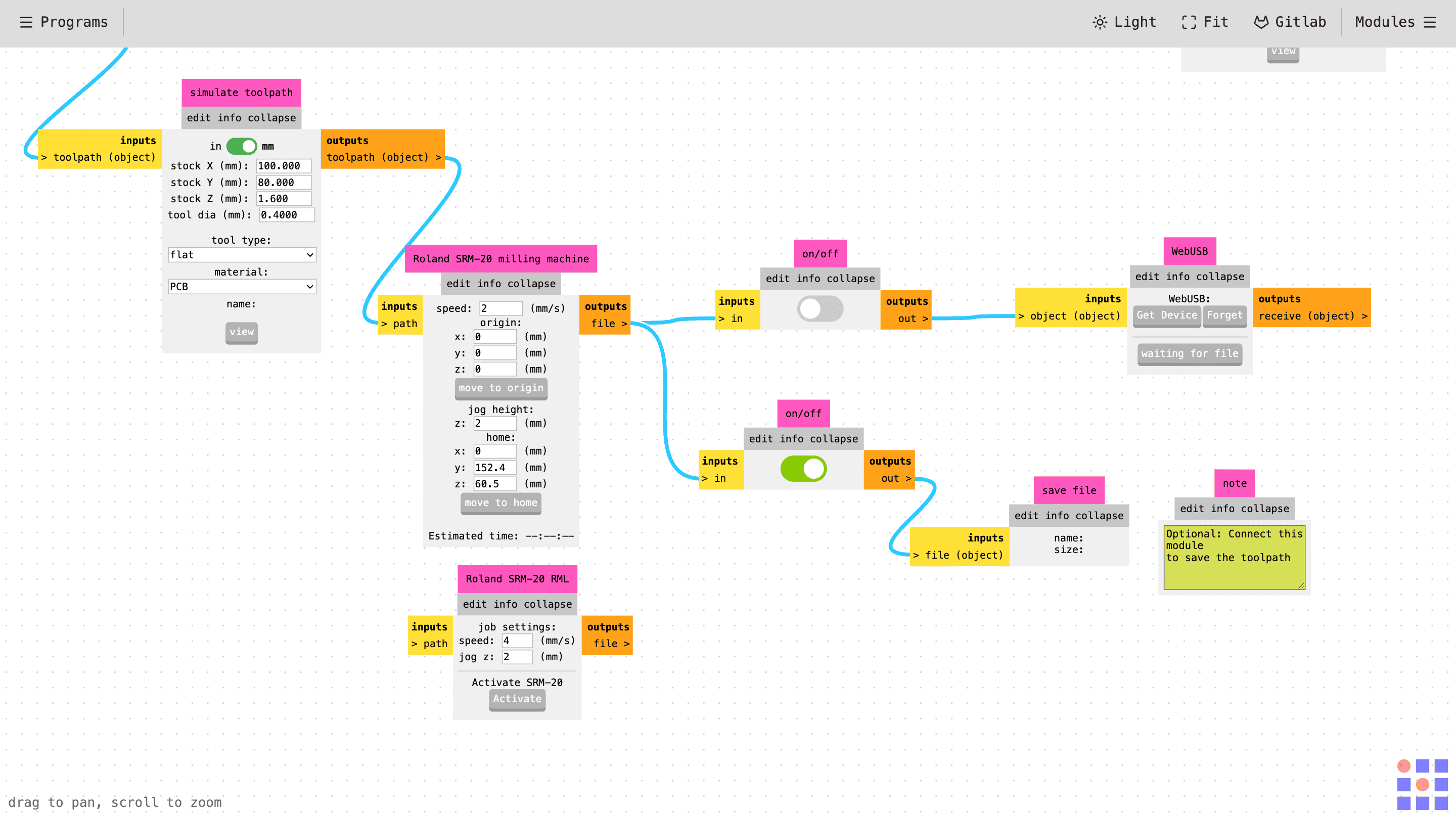
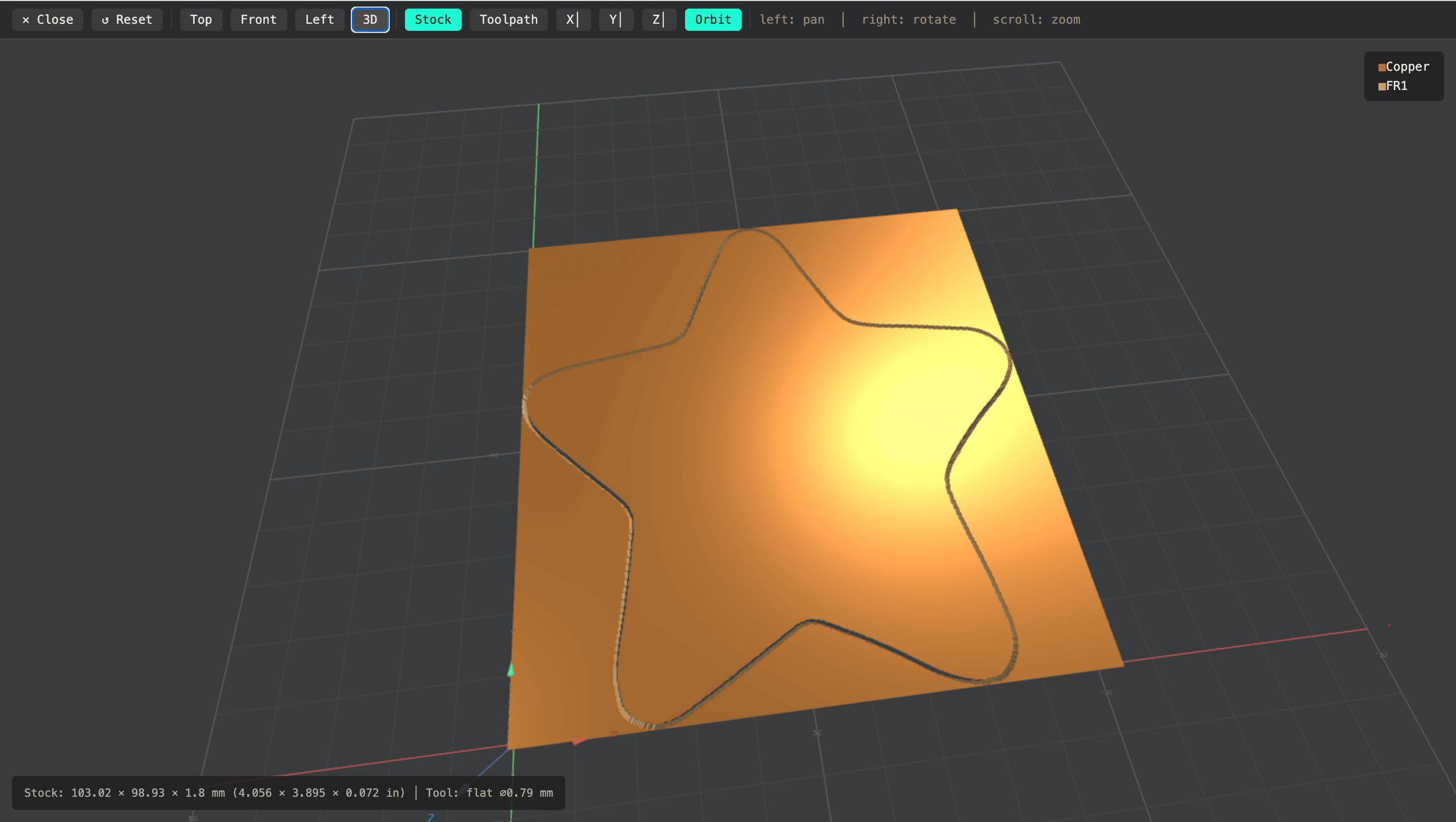
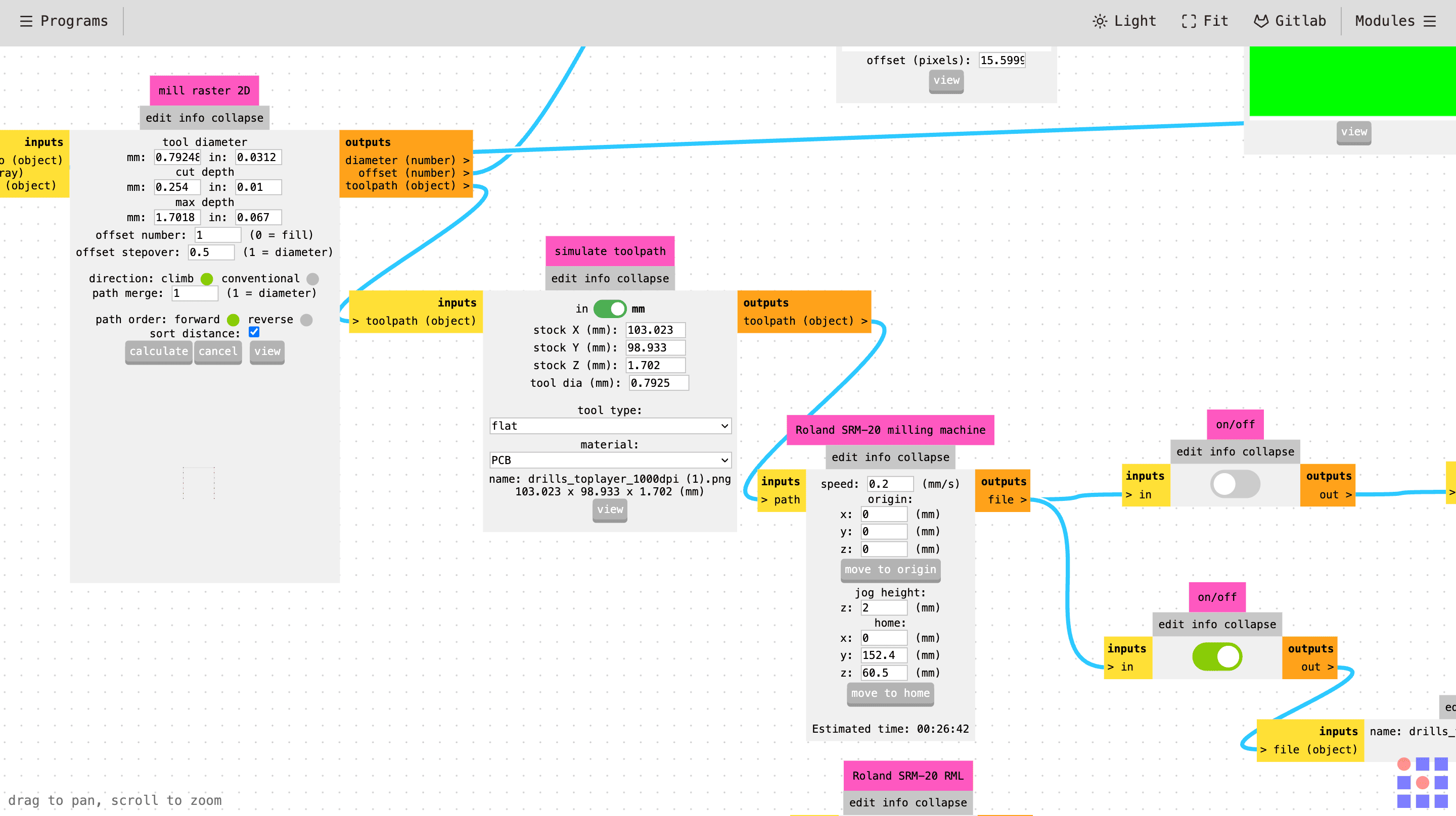
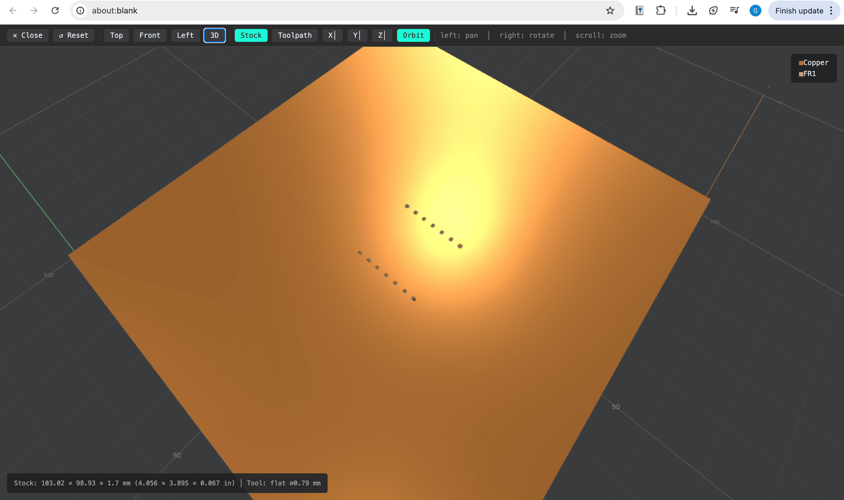
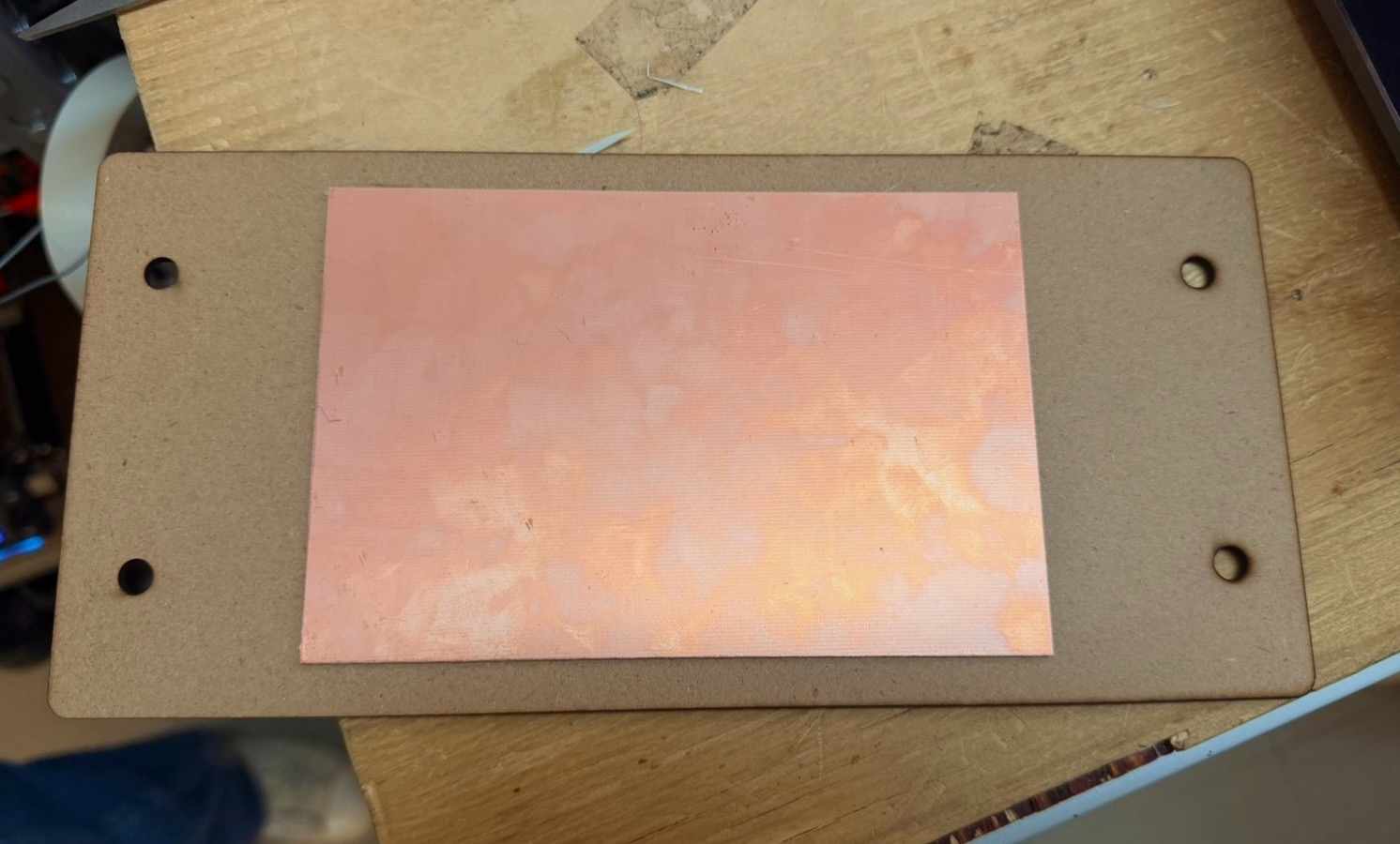
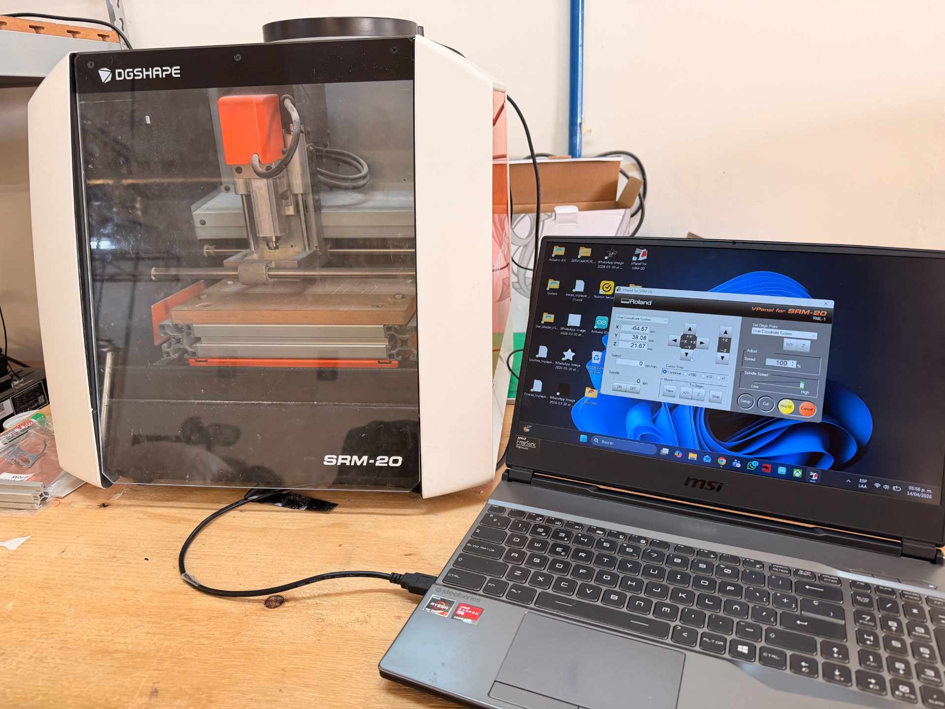
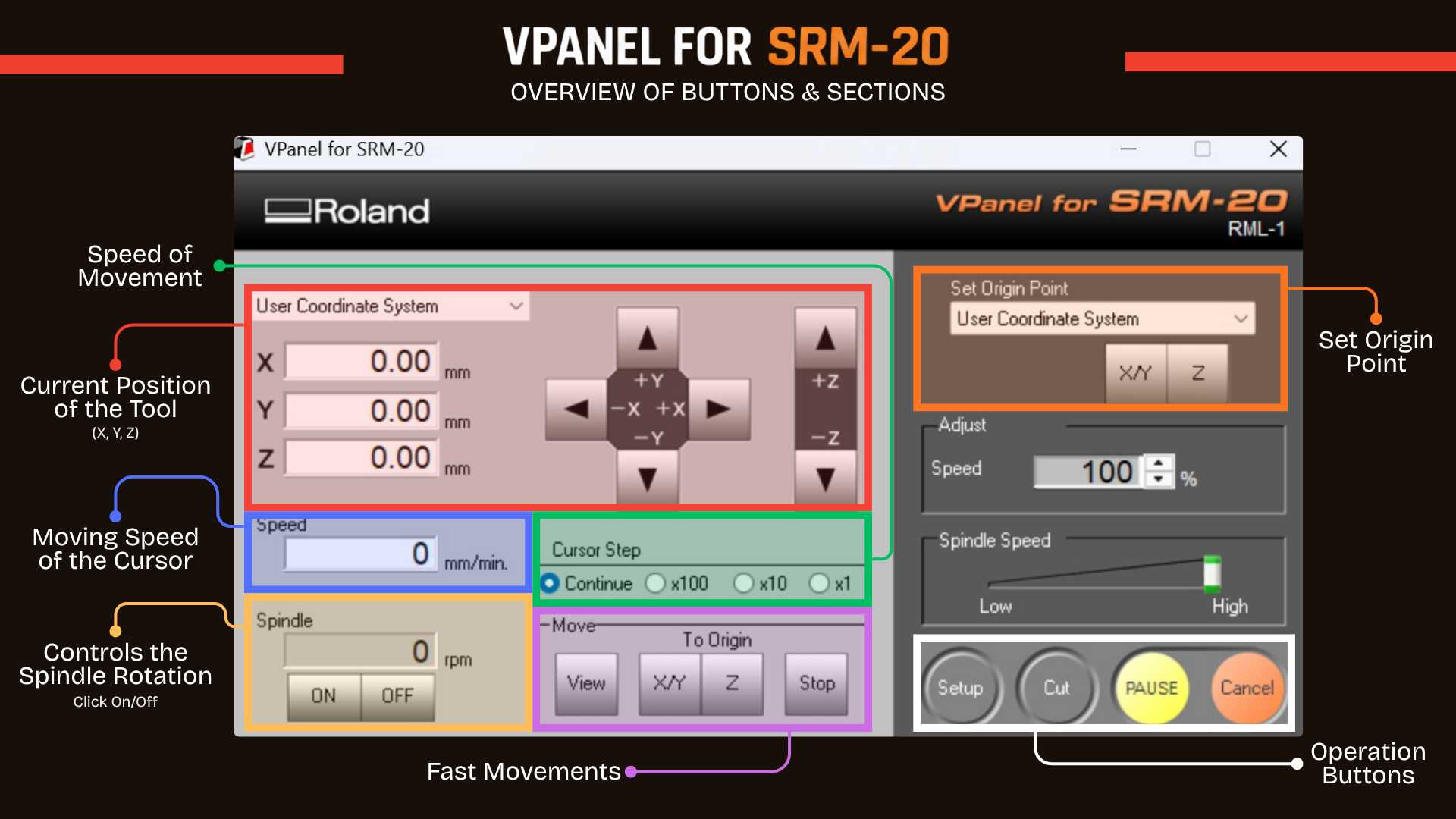
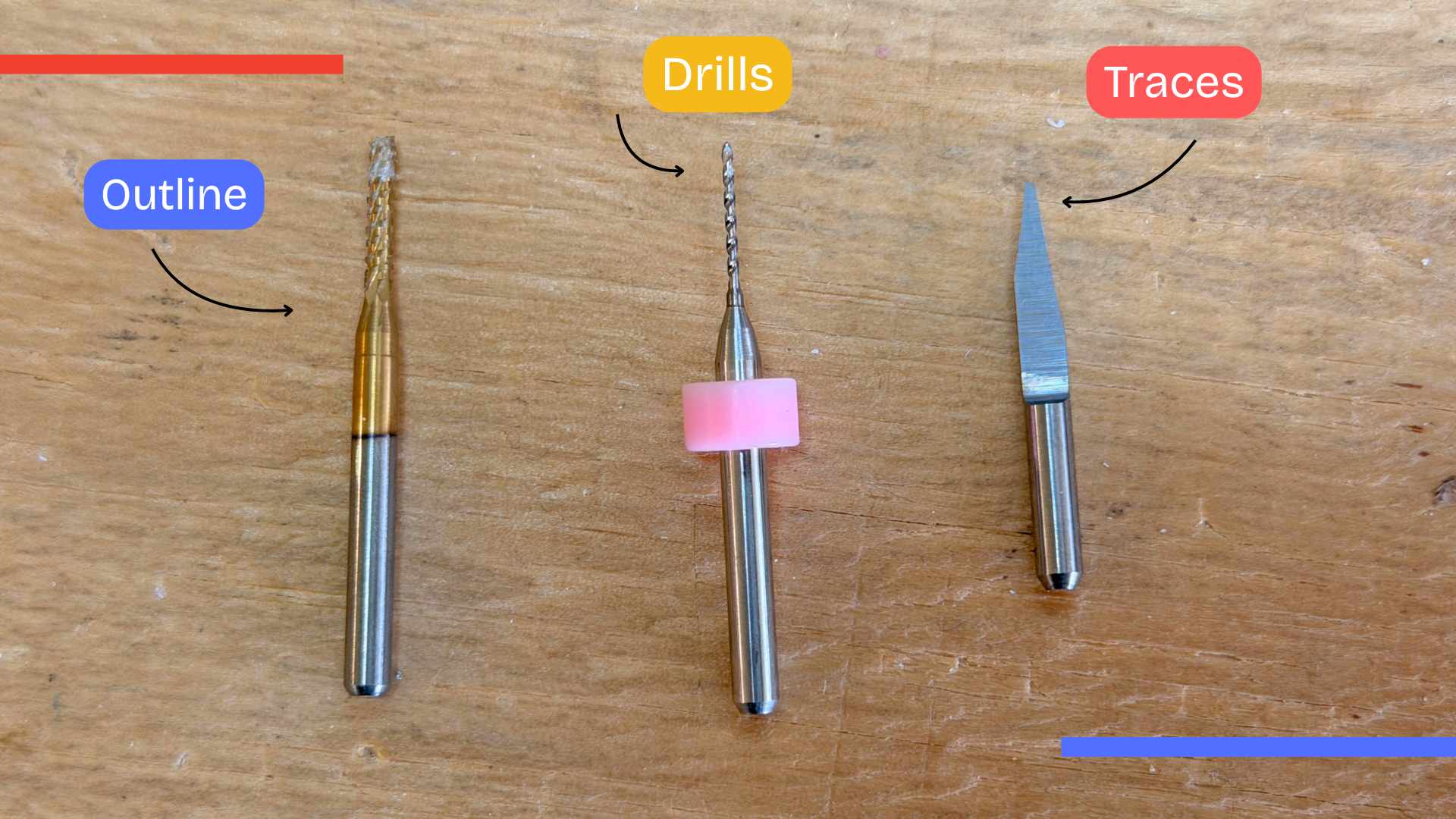
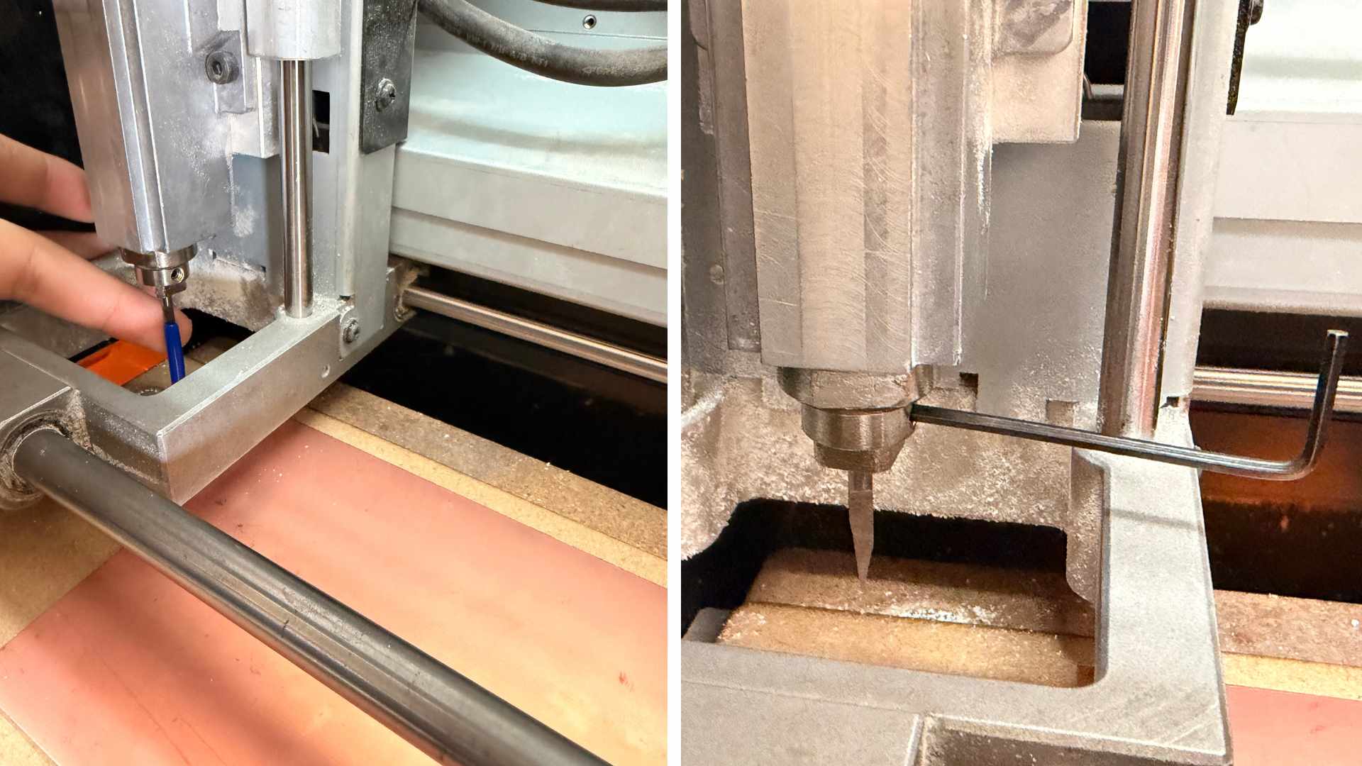
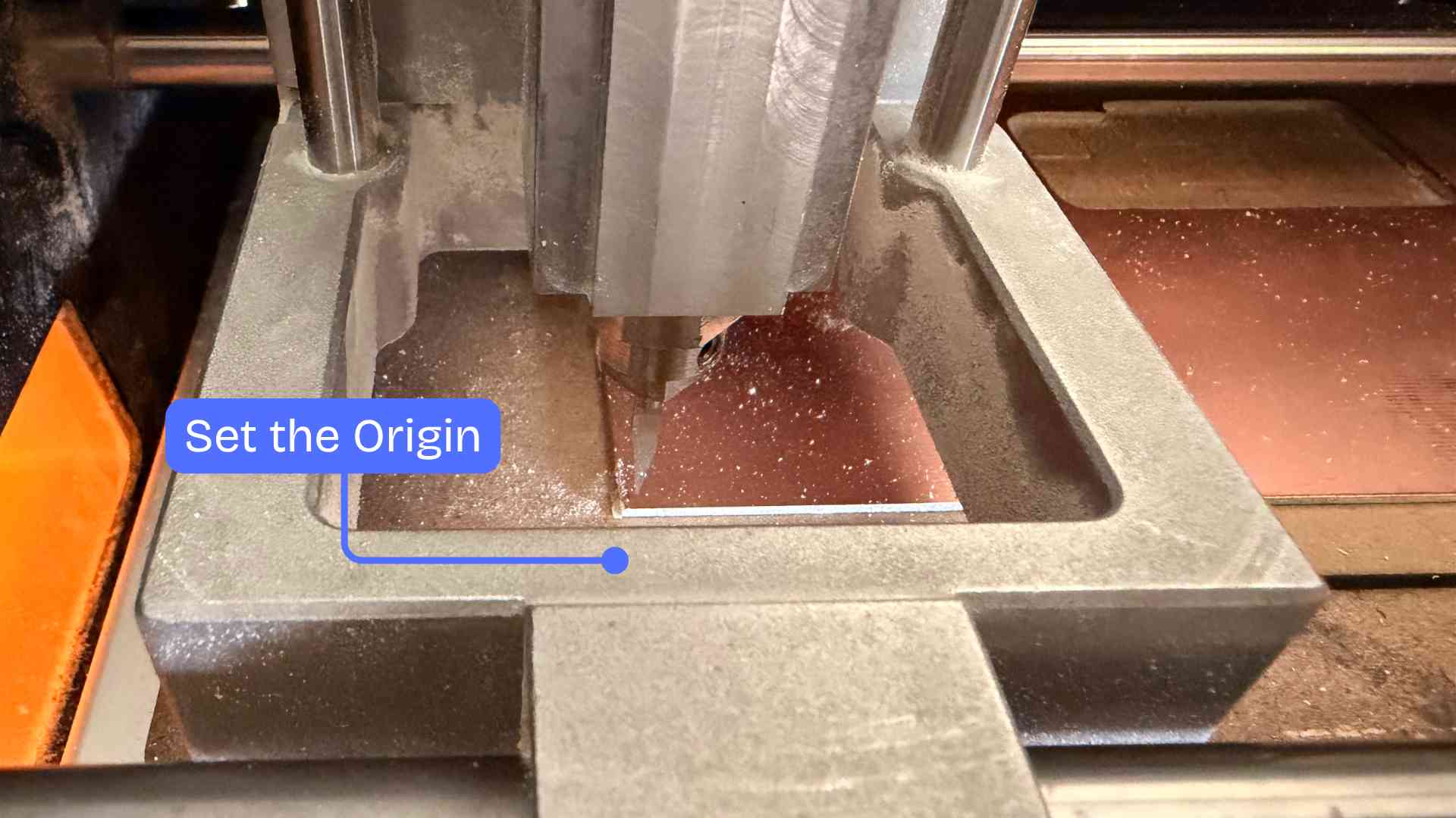
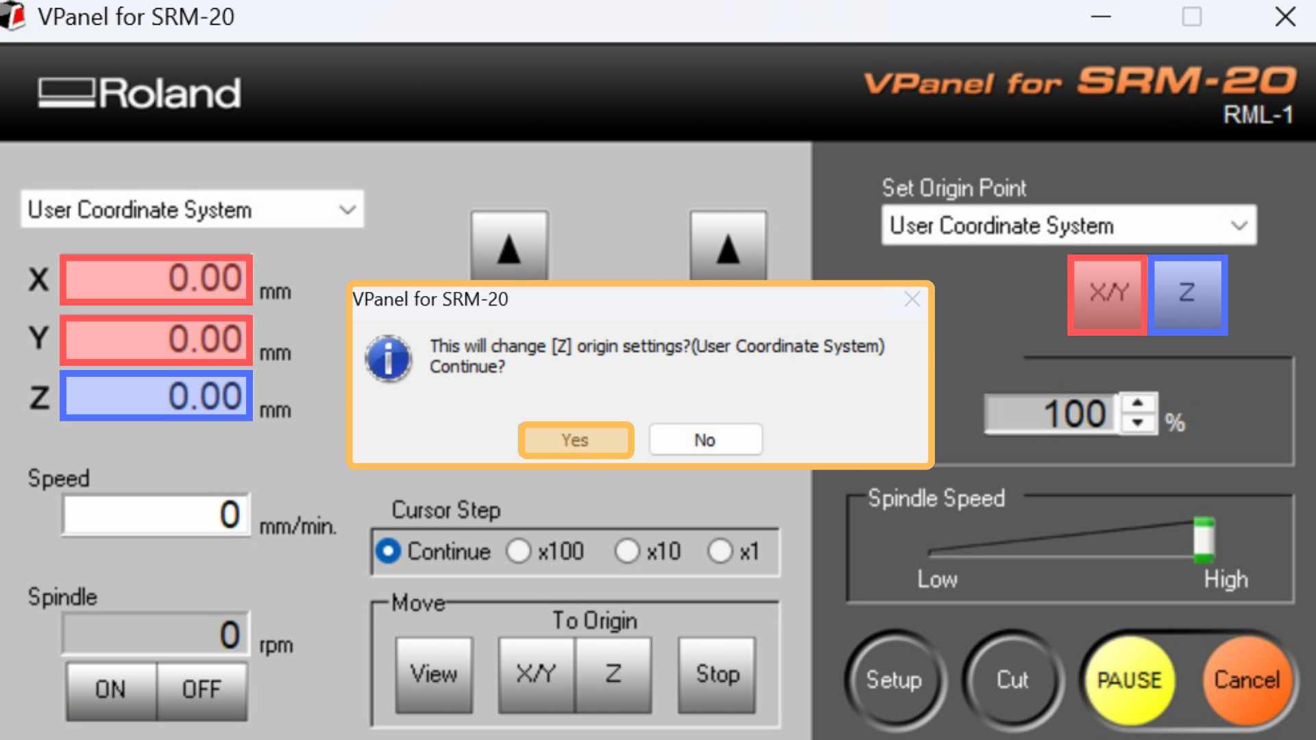
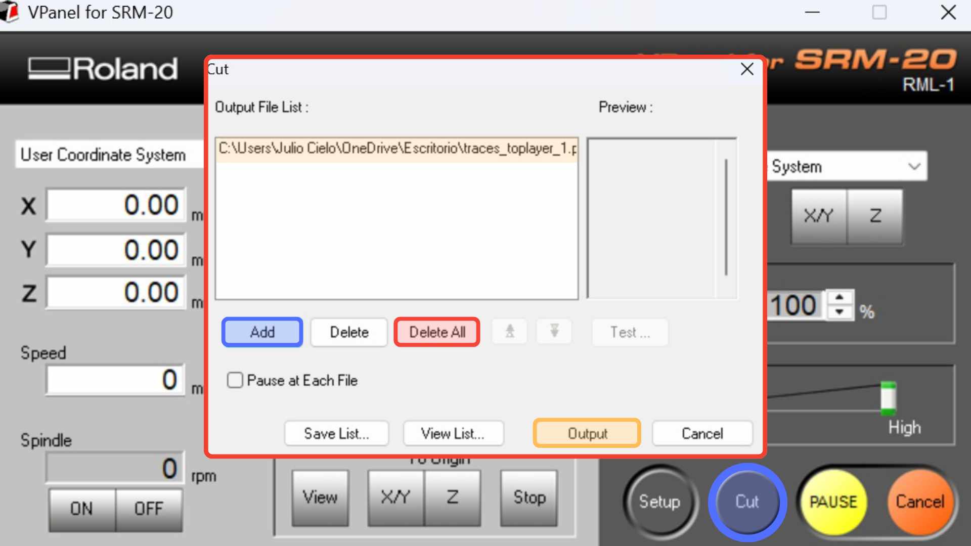
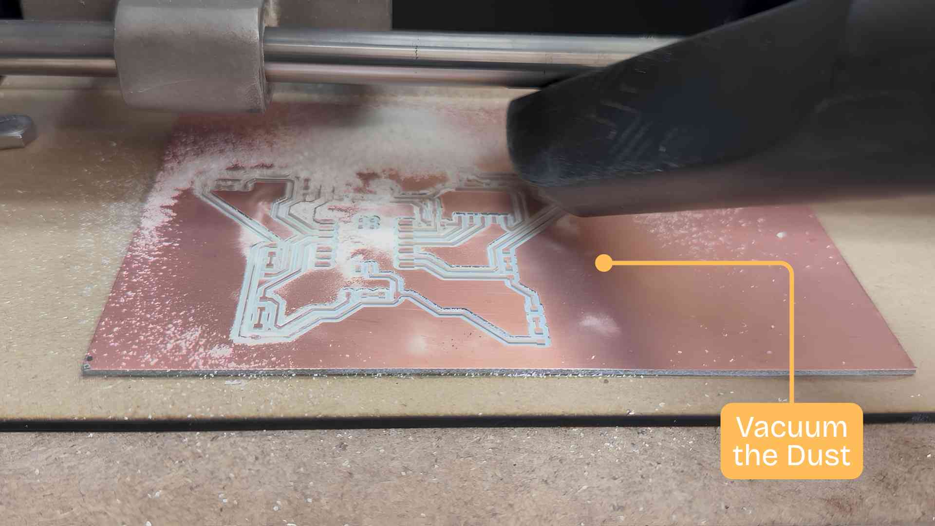
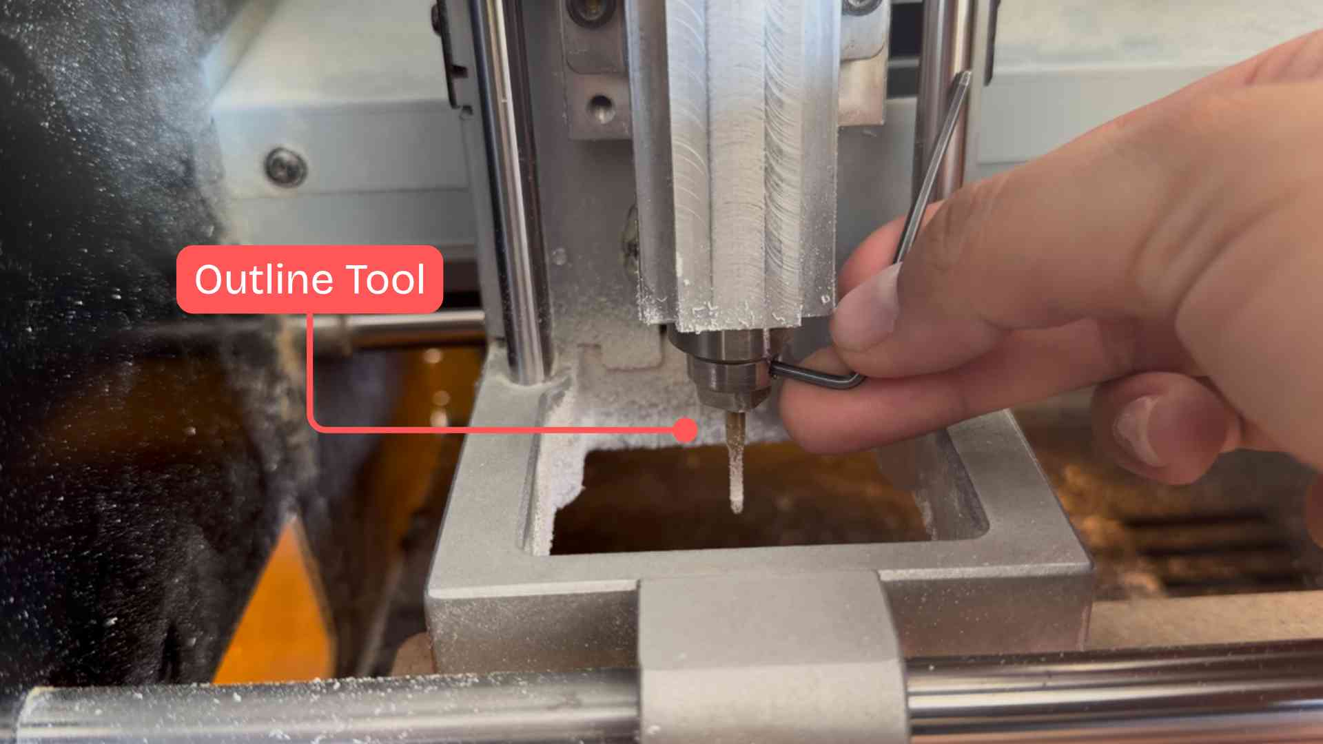
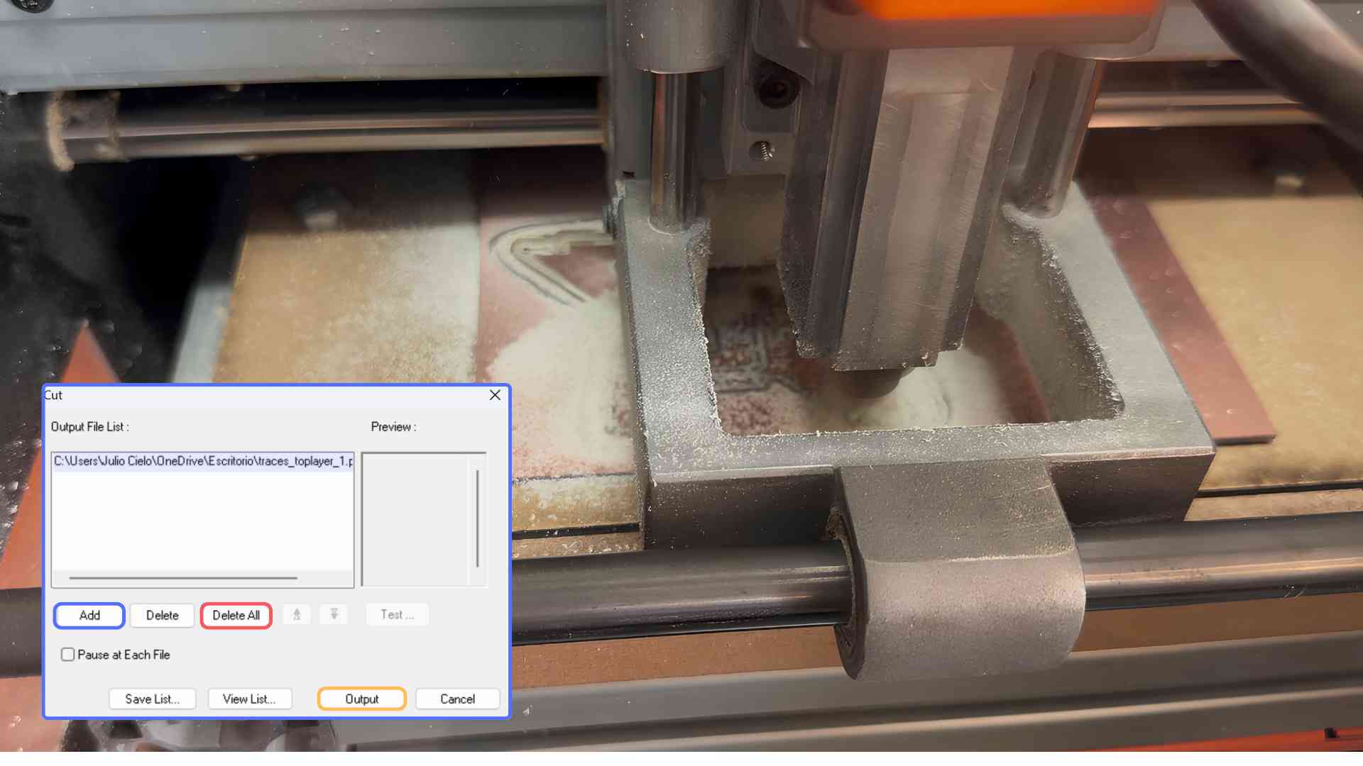
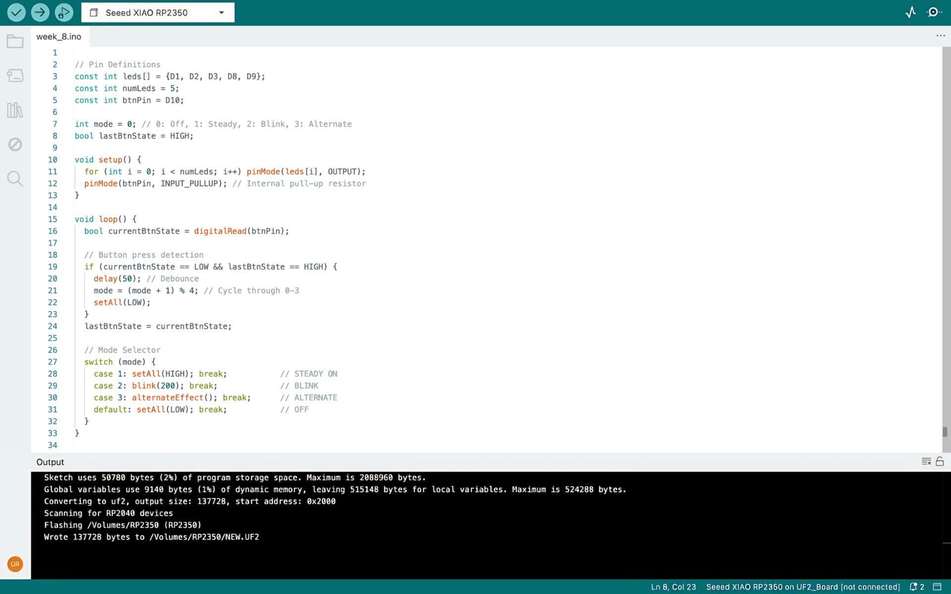
This week focused on transforming a digital PCB design into a functional physical board. Starting from the refinement of my previous design, it was also necessary to prepare the files for fabrication, mill the PCB using the Roland SRM-20, and assemble it through soldering. Finally, the board was programmed to verify its functionality, completing the transition from design to working electronics. For this, I consulted our Group Assignment.

◆ Schematic Review & Adjustments

Before fabrication, I reviewed my PCB design from Week 6 to confirm it was ready for production. While the board was already functional, I made a few key adjustments: I enabled additional pins on the Seeed Studio XIAO RP2040 to support future I2C and UART communication, and I repositioned the push button to ensure proper clearance for the USB-C cable, improving both usability and assembly.

Pinout Diagram

✦ Updated Schematic

The design includes ten LEDs grouped in pairs, each with 220Ω resistors. The previous button was replaced with a Switch Tactile CNK, and a capacitor was added for power stabilization. Power distribution is defined through 3V3 and GND labels with PWR_FLAG symbols. Additionally, pin headers for I2C (SDA, SCL with 4.7kΩ pull-up resistors) and UART (TX/RX) were included for future expansion.

◆ What I will be using?

✦ PCB Design

Once the schematic was completed and verified, the design was transferred to the PCB editor in KiCad. Since this board was based on a previous development, the PCB layout was reused and adjusted to the new components.

Pinout Diagram

✦ Board Setup

The layout was also developed following a star-shaped outline, and the outline of the board was defined with a thickness of 2 mm. On the other hand, the routing was carried out using 0.8 mm minimum track width and a 0.7 mm minimum track clearance; ensuring suitable connections for the milling process.

Pinout Diagram

✦ Gerber Files

Once the PCB design was completed, the files were prepared for fabrication. For this I exported my files to Gerber, which is used to define each layer of the PCB and its corresponding traces. For this, I went to the option File → Fabrication Outputs → Gerber Files. A configuration window appeared and then click on Plot.

After completing the export process, the program creates a folder containing all the generated Gerber files, which I will be using for the next fabrication steps.

✦ Conversion of Geber Files to PNG Images

For this step I will be using the gerber2png. I selected all my Gerber Files and uploaded them to the page. Once the files were uploaded, the platform displayed the available layers, such as Top Trace, Top Drill and Top Cut. I clicked on Generate All to produce the corresponding images, then click on “generate PNG”.

✦ Configuration in Mods

For the cutting process I will be using the Roland SM-20 Milling Machine , and to set up its parameters I used modsproject.org, a platform that allows the adjustment of key settings required for the fabrication process.

✦ Roland SRM-20 Setup

✦ Milling Process

✦ Soldering Process

✦ Programming