✦ Introduction to Electronics Design
This week I focused on understanding the fundamentals of electronics design and learning how to develop a custom PCB using the KiCad software. Personally, this week was quite challenging since I don't have a very strong background in electronics. However, it was very interesting to explore how electronic components connect and how circuit designs are translated into physical boards. Also, for this week I reviewed some electronic concepts in the Group Assignment.
✦ Learning about Electronics
Current
Flow of electrons through a conductor, measured in amperes (A).
Voltage
Electrical potential difference that pushes current through a circuit.
Resistance
Opposition to the flow of current, measured in ohms (Ω).
LEDs
Light-emitting components that require a resistor to limit current.
✦ Electronics Design Workflow
- 1.Define the circuit function
- 2.Create the schematic diagram
- 3.Assign footprints to components
- 4.Convert the schematic into a PCB layout
- 5.Route the connections between components
- 6.Generate 3D visualization and fabrication files
✦ Designing my PCB
For this assignment, I designed a custom PCB shaped like a star. The main function of this was to create an interactive light display, using the XIAO RP2040 microcontroller that acts as the brain of the circuit, reading an analog signal from the potentiometer. By turning the potentiometer, the user can dynamically control the LEDs, such as adjusting their brightness.
1x Seeed Studio XIAO RP2350
Runs the code and manages the inputs and outputs.
1x Potentiometer
An analog input used to control LED parameters.
1x Push Button
A digital input used to trigger specific actions.
1x Capacitor 1206 SMD (100nF)
Filters noise and stabilizes the microcontroller power supply.
10x LEDs SMD
Distributed around the star shape for the visual lighting effects.
10x Resistors (220Ω)
Protect each LED by limiting the flow of current.
1x Custom Star-Shaped PCB
The designed board that integrates all these components.
✦ What is a Pull-up & Pull-down?
A pull-up resistor keeps the pin at HIGH by default, a pull-down keeps it at LOW. Both exist to avoid random, unpredictable readings when the button is not pressed. This design uses a Pull-up because the button is connected to GND, so when pressed it pulls the pin LOW.
✦ Install KiCad
The first step was creating the Schematic in KiCad. In this stage, the electronic connections between components are defined without considering their physical placement.
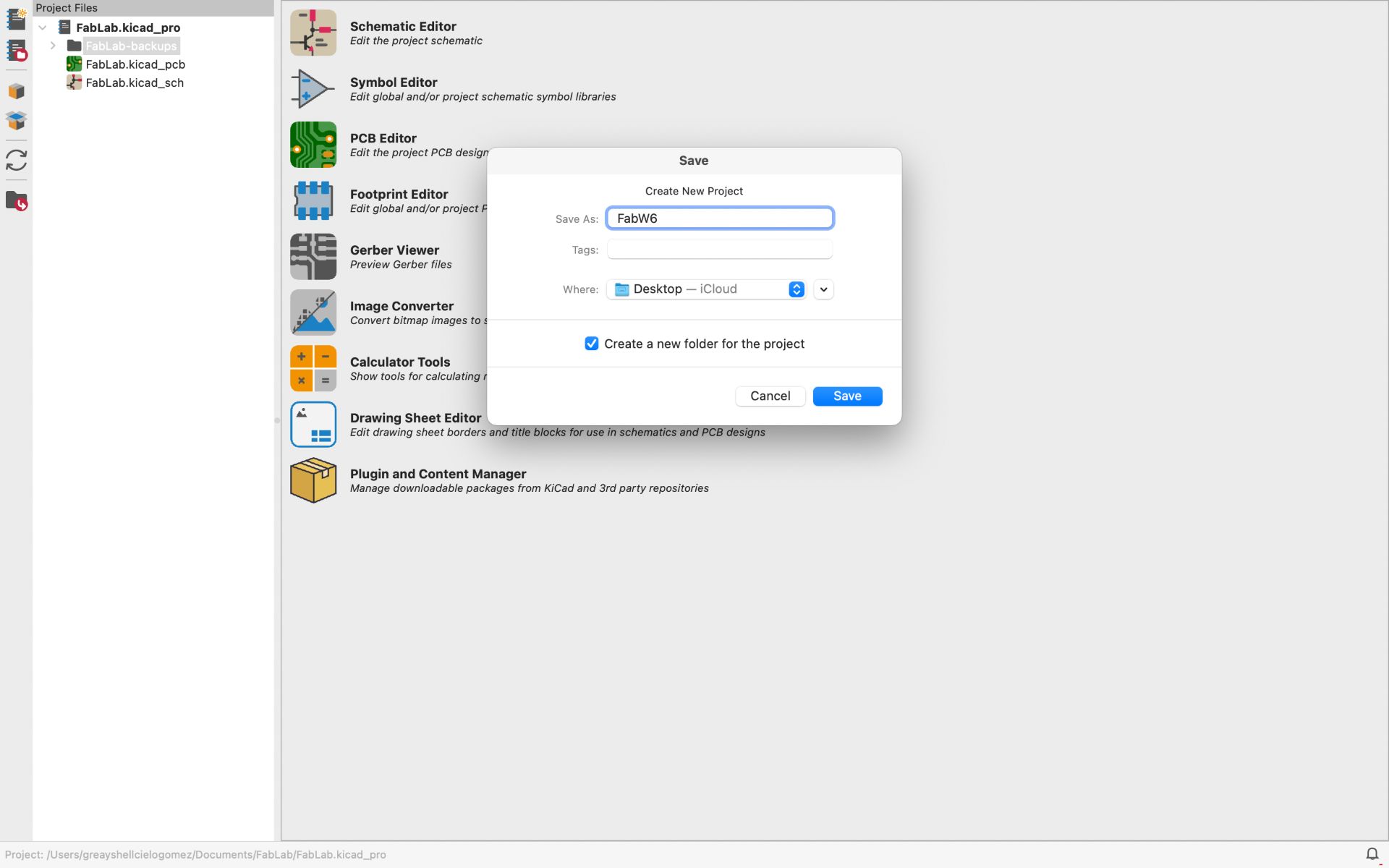
01. CREATING A NEW PROJECT
To begin, I created a new project in KiCad. I navigated to File → New Project → Save As, and saved the project as FabW6.
02. SCHEMATIC EDITOR & PCB EDITOR
After creating and saving the project, the Schematic Editor and PCB Editor tabs appeared automatically on the left side.
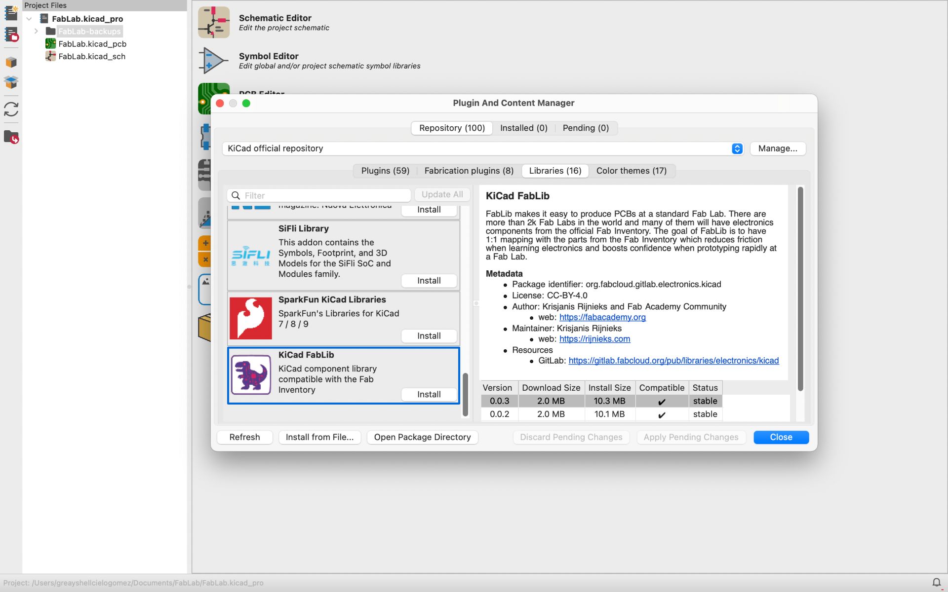
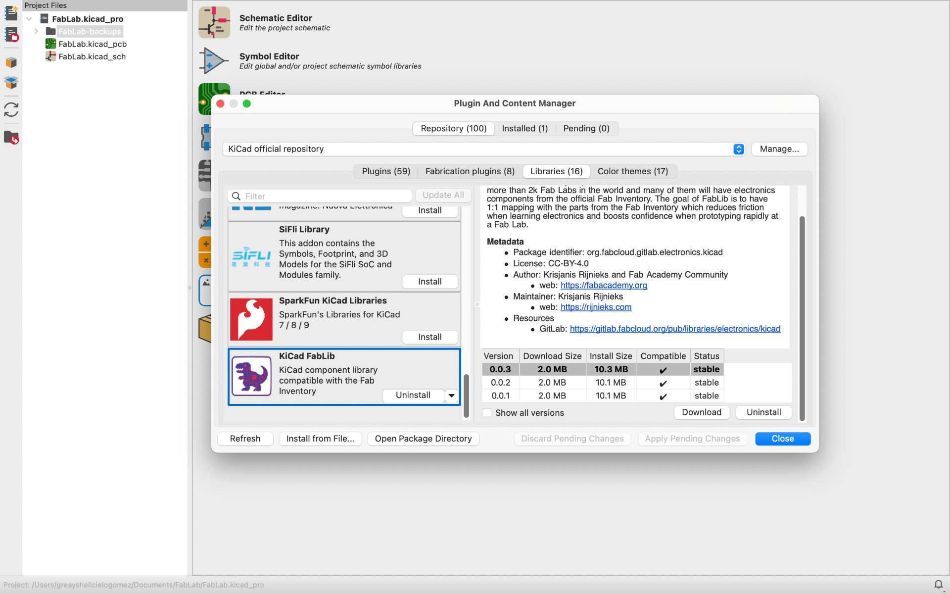
03. INSTALL THE FAB ACADEMY LIBRARIES
Next, I installed the libraries provided by Fab Academy. To do this, I went to Preferences → Manage Symbol Libraries → Plugin and Content Manager → Libraries. Then, I searched for KiCad FabLib, selected it, and installed it.
0.4 OPENNING THE SCHEMATIC EDITOR
After a couple of minutes, the library was successfully installed. Then I closed the window and began the schematic design by double-clicking on the “Schematic Editor”.
❮
❯
✦ Schematic Editor
The first step was creating the Schematic in KiCad. In this stage, the electronic connections between components are defined without considering their physical placement yet.
01. ADDING COMPONENTS
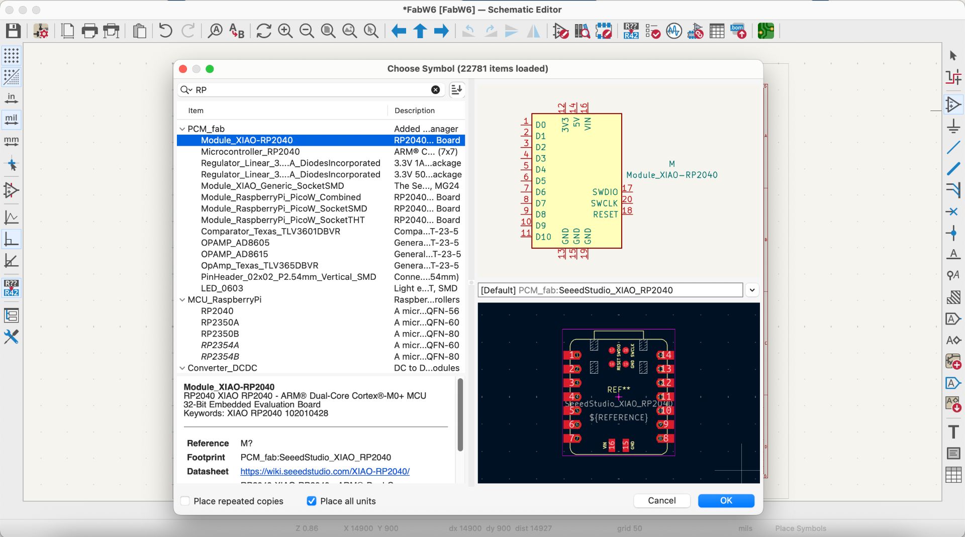
Once inside the Schematic Editor, a blank workspace appears along with several tools on the side panels that help with the schematic design. To start adding components, I pressed the “A” key on the keyboard, which opened a window displaying the available symbols.
02. SELECTING COMPONENTS FROM THE LIBRARY
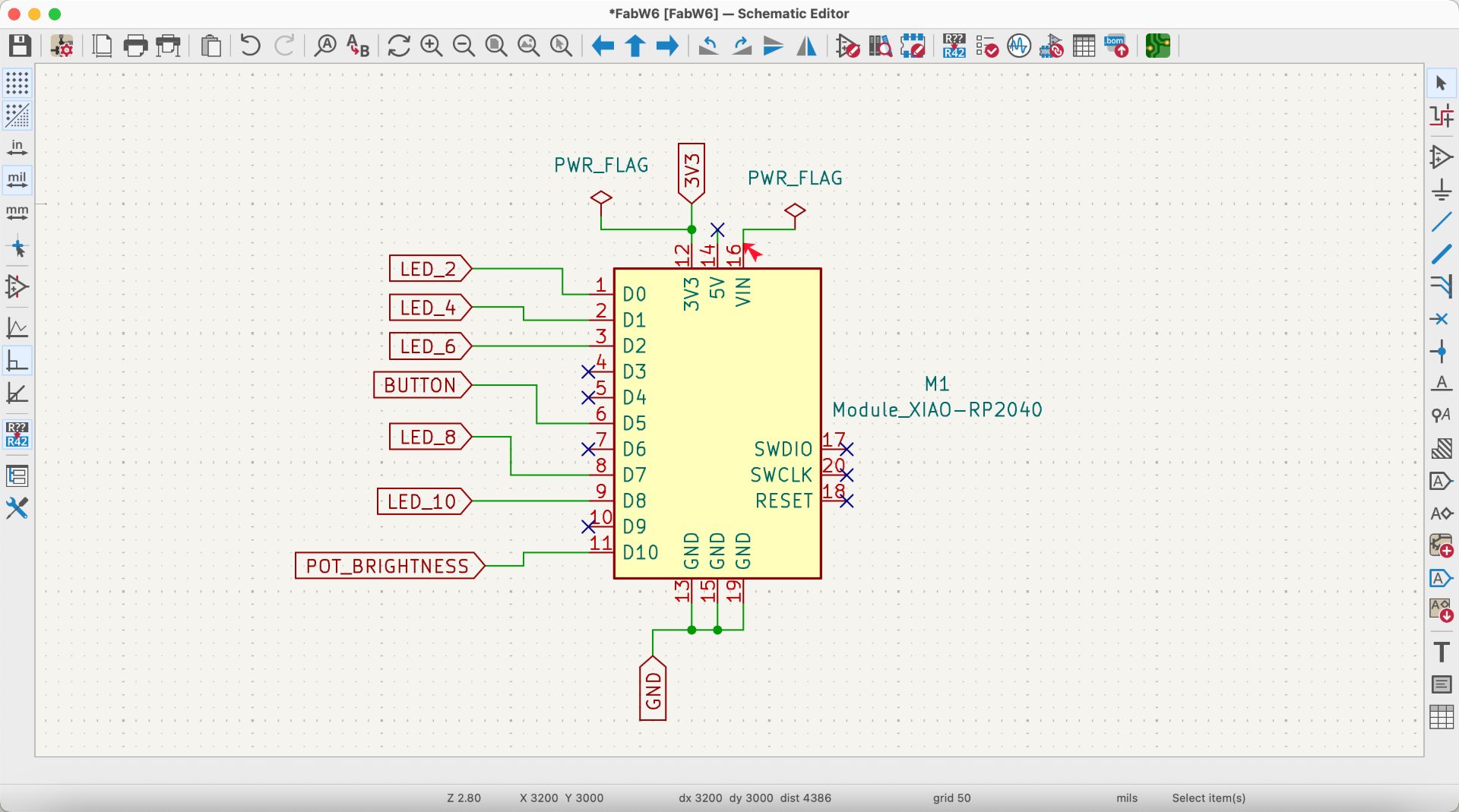
In the symbol menu, all the components from the library are displayed, each with a corresponding footprint. For this assignment, I used a XIAO RP2040 microcontroller, which I added using the search bar in the symbol window.
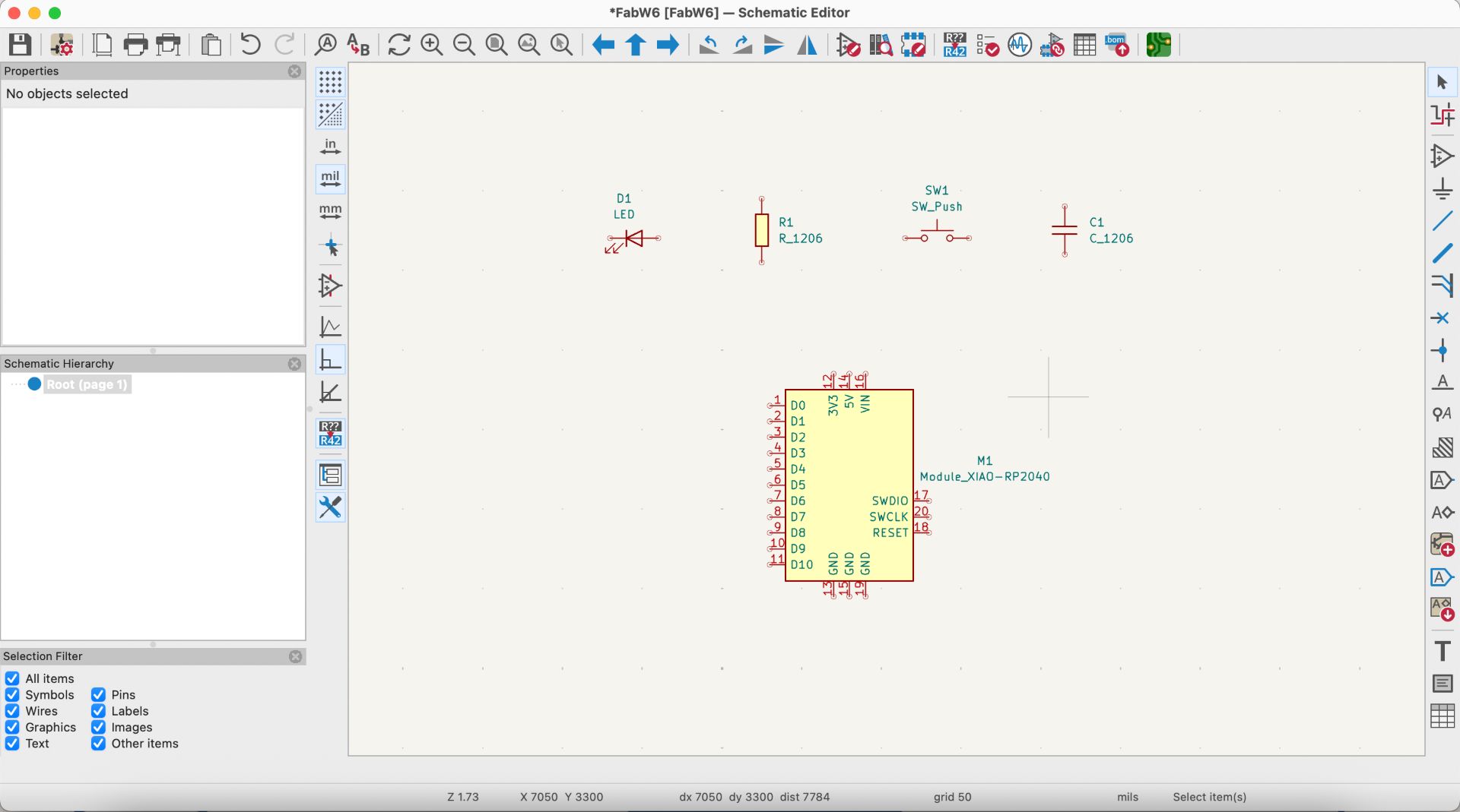
03. PLACING THE REQUIRED COMPONENTS
The same process was repeated to place all the components needed for my schematic design.
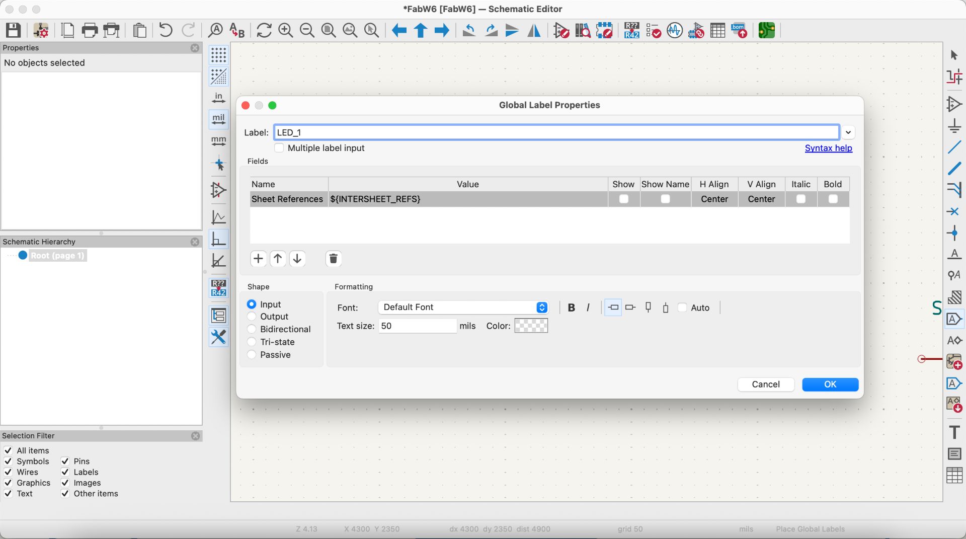
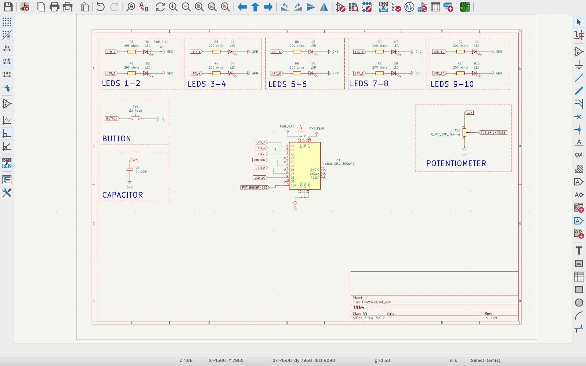
04. USING LABELS FOR ORGANIZATION
To keep the schematic organized, I assigned labels to the components using Cmd + L. These labels also allowed me to connect components to the microcontroller without using physical wires, which helps keep the schematic cleaner and easier to understand.
05. ORGANIZING COMPONENTS INTO BLOCKS
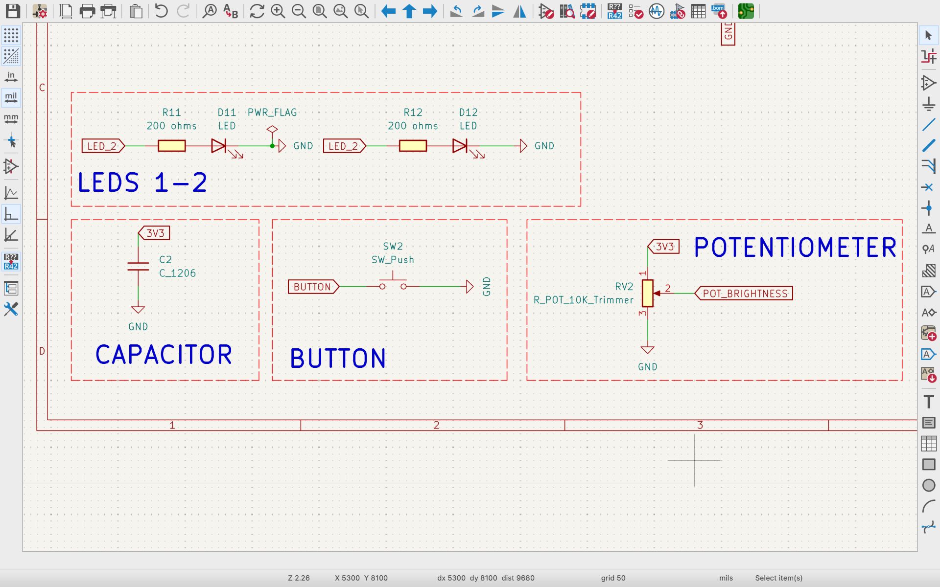
I grouped the components into individual blocks and used the text tool to add labels that identify each section. In total, I created five LED blocks. Each block contains two LEDs, since my PCB requires ten LEDs in total, but the microcontroller does not have enough GPIO pins to control each LED individually. Grouping them this way helped maintain better organization and control of the LEDs.
06. WIRING COMPONENTS
wiringAfter organizing the components, I connected the labels of each block to the XIAO RP2040. In the image below, the distribution of the LEDs, potentiometer, and the 3V3 power supply connected to the microcontroller can be observed.
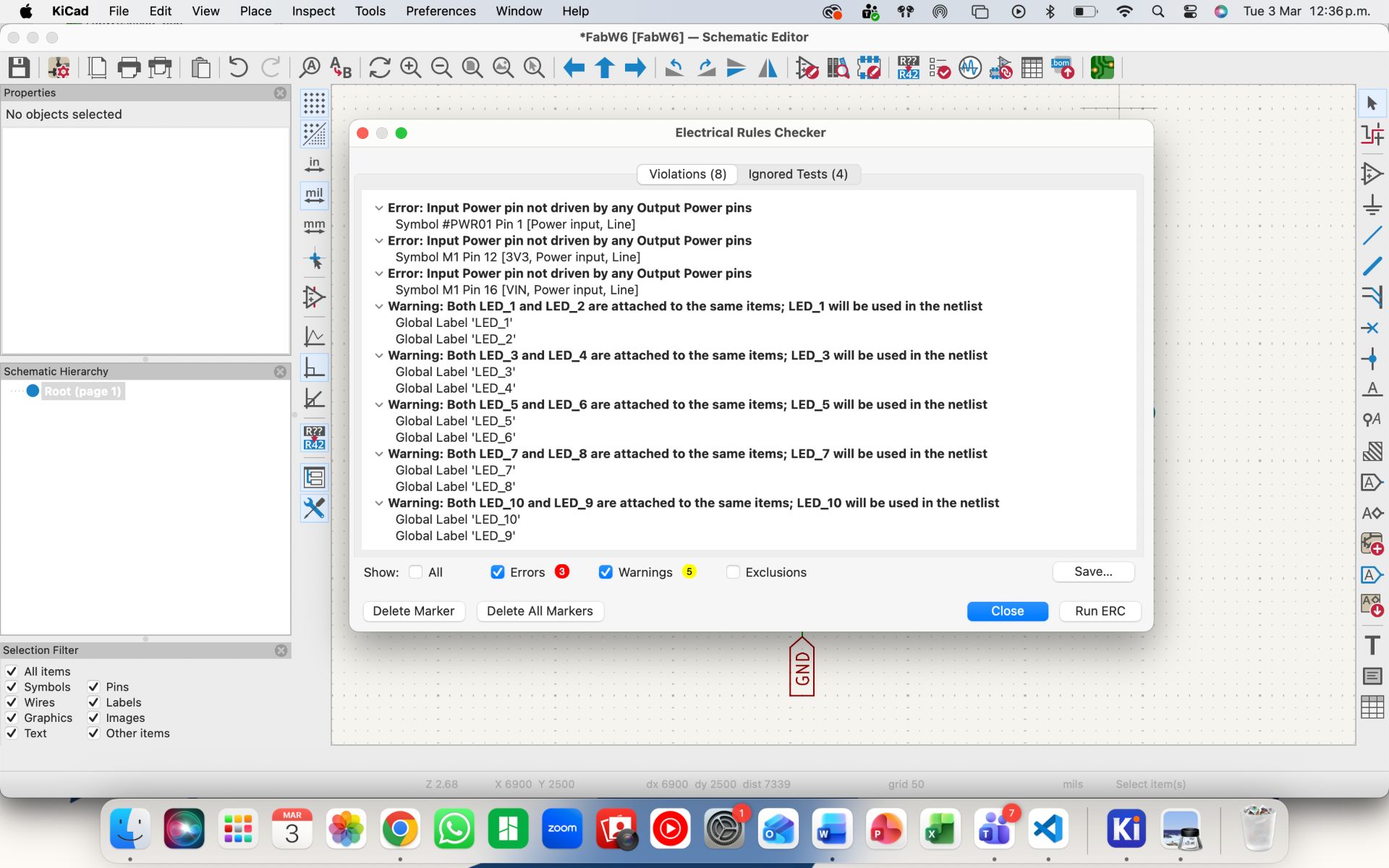
07. RUNNING THE ELECTRICAL RULES CHECK (ERC)
Once the schematic was completed, I verified that all components and connections were correct by running the ERC. To do this, I went to Inspect → Electrical Rules Checker → Run ERC. The system detected three errors in the schematic, so I reviewed the circuit and corrected the issues.
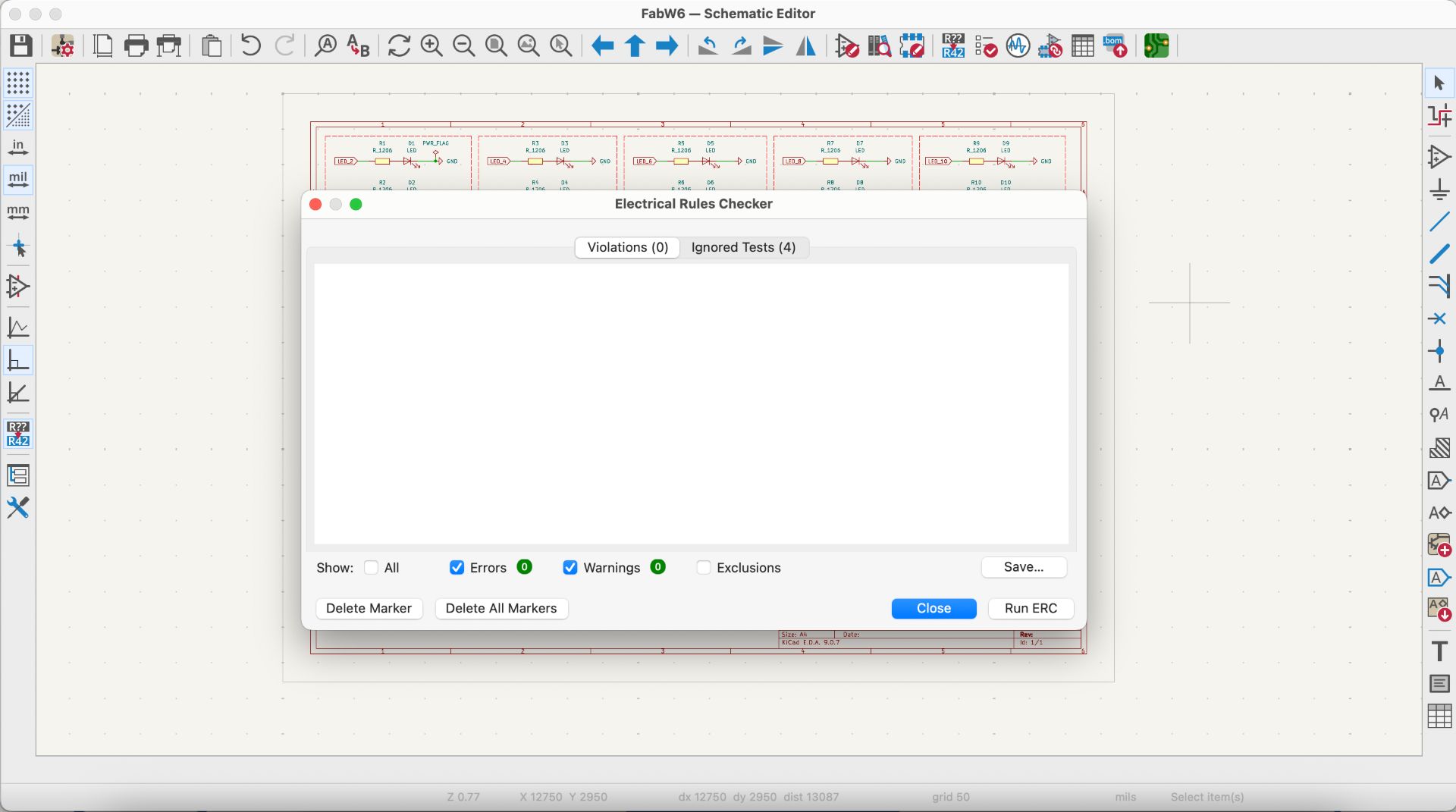
08. VERIFYING THE CORRECTED SCHEMATIC
After making the necessary corrections, I ran the ERC again. This time, no errors were detected, only a few warnings that can safely be ignored. With the schematic verified, the design was ready to move on to the PCB Editor for the layout stage.
09. FINAL SCHEMATIC
This is the final schematic design showing all the components of the PCB and their corresponding connections.
❮
❯
✦ PCB Layout
The first step was creating the Schematic in KiCad. In this stage, the electronic connections between components are defined without considering their physical placement.
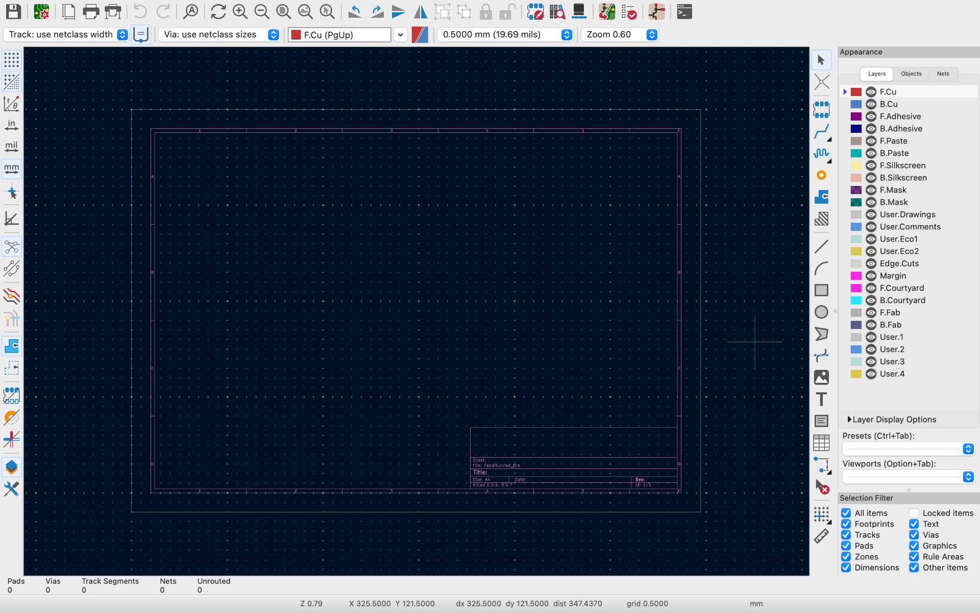
01. OPENING THE PCB EDITOR
To open the PCB Editor, I went to the main KiCad window and double-clicked the PCB Editor icon. A black workspace appears where the PCB layout will be created.
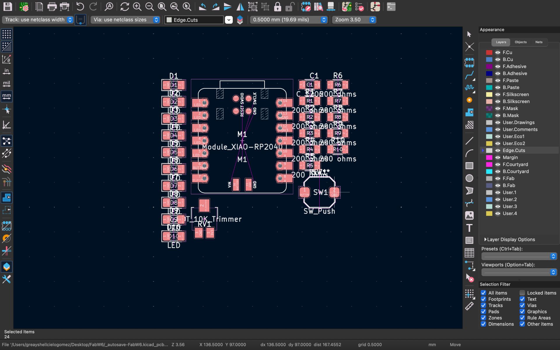
02. UPDATE PCB FROM SCHEMATICS
To import the schematic into this workspace, I clicked the Update PCB from Schematic icon located on the top toolbar (the icon showing half schematic and half PCB). All the components from the schematic appeared grouped together. To place them on the board, I clicked on the area where I wanted them to be positioned.
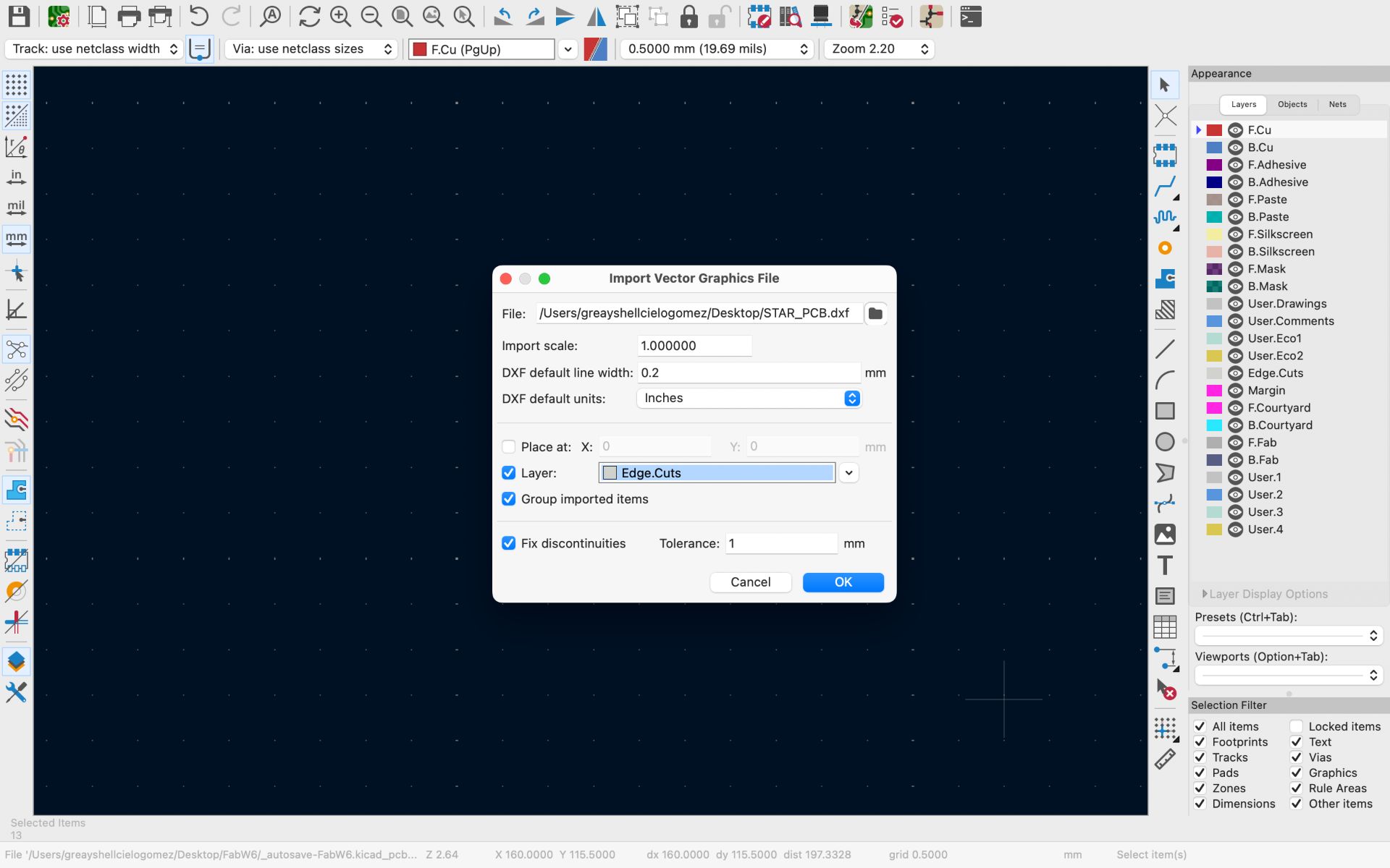
03. IMPORTING STAR SHAPE
Since I wanted my PCB to have a star shape, I first created the outline in Adobe Illustrator and exported it as a .dxf file. Then in KiCad I went to File → Import → Graphics, selected the file, and adjusted the scale. In my case, the correct scale value was 0.165.
04. POSITIONING THE STAR
The star shape appeared on the workspace and was positioned around the components to begin organizing the layout.
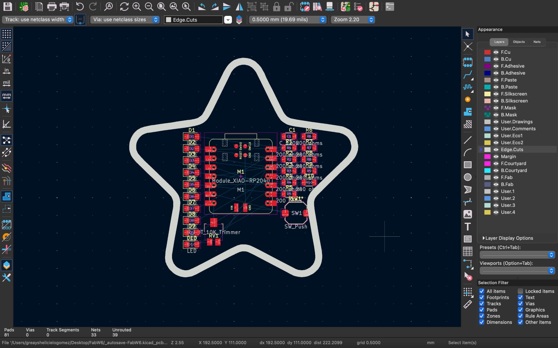
05. PLACING THE COMPONENTS
I arranged the components inside the star, placing the LEDs around the edges of the shape. Each LED was paired with a 200 Ω resistor, while the microcontroller was placed in the center. Other components such as the potentiometer, button, and capacitor were positioned in the remaining spaces.
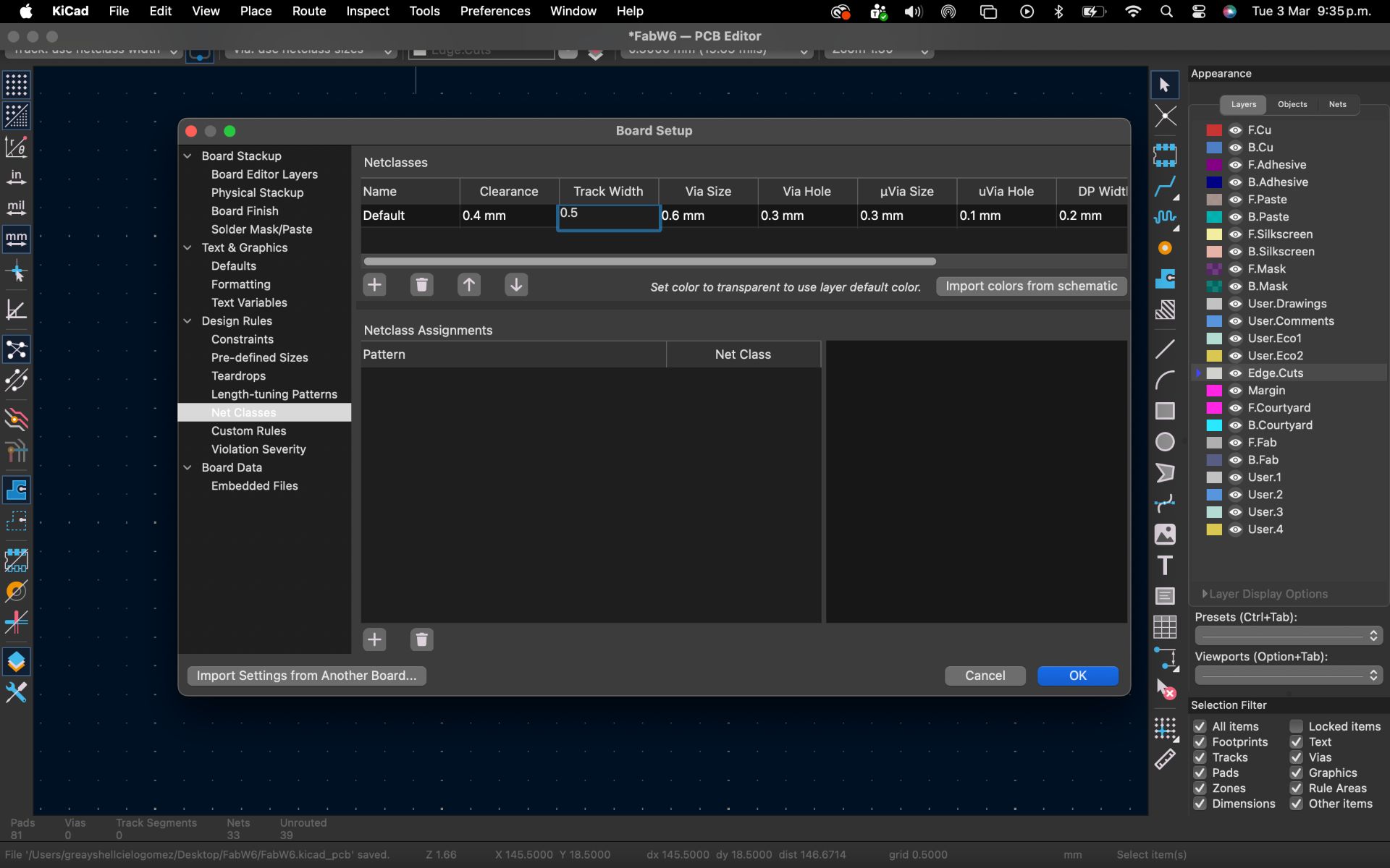
06. DEFINING DESIGN RULES
I defined a Track Width of 0.5 mm and a Clearance of 0.4 mm in KiCad’s Design Rules. These settings ensure proper electrical connections and help prevent short circuits, allowing the DRC (Design Rule Check) to validate the design.
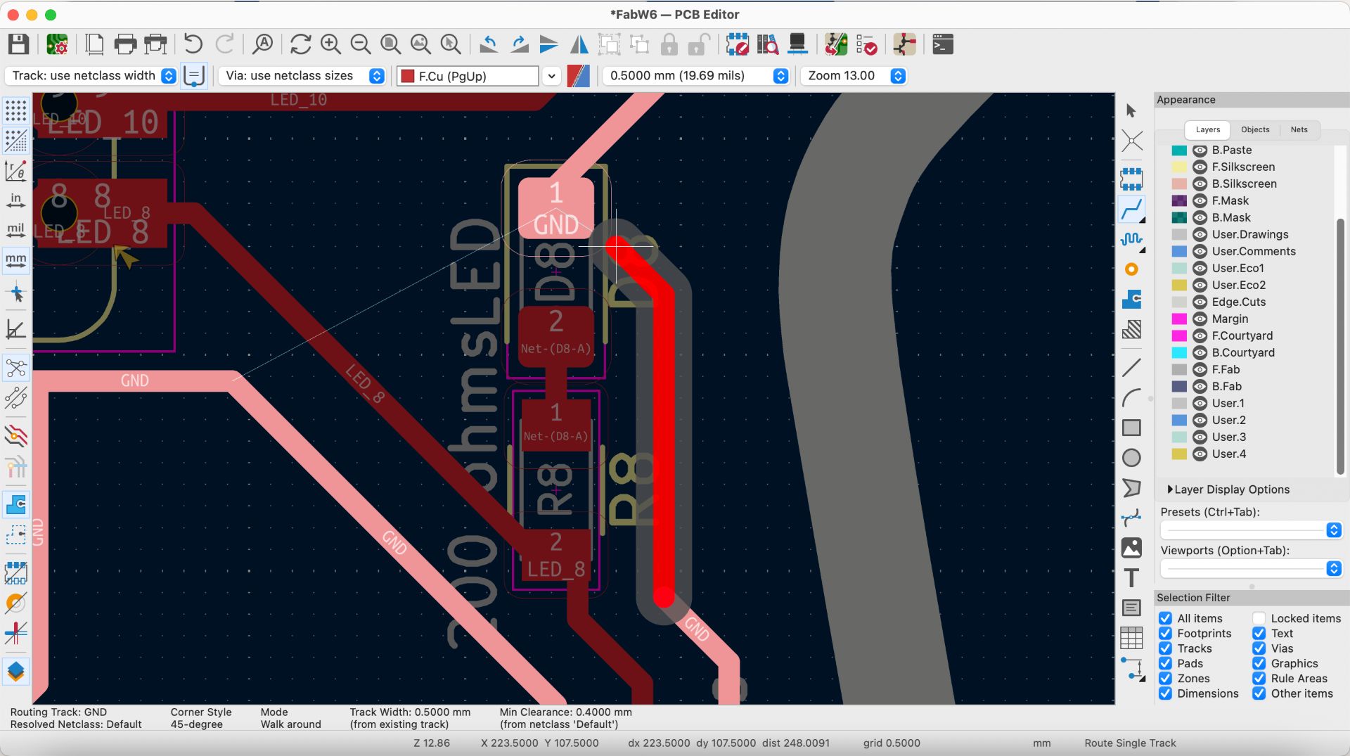
07. ROUTING
Using the “W” key, I started routing the connections between the components and the microcontroller. During this process, I frequently adjusted the orientation and position of the components to make the routing easier and avoid crossing traces.
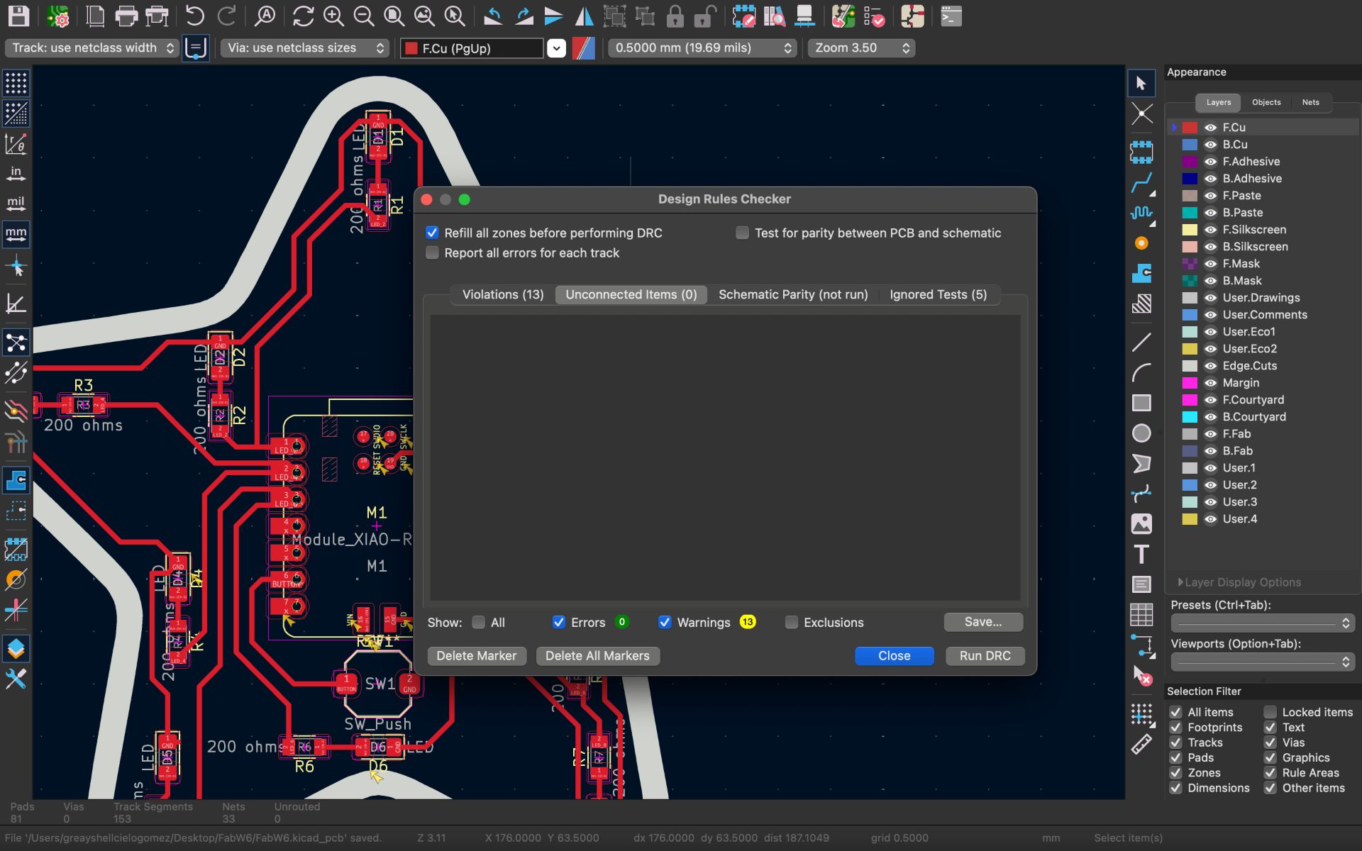
08. RUNNING DRC
Once the routing was completed, I ran the Design Rule Check (DRC) by going to Inspect → Design Rules Checker → Run DRC. Initially, a few errors appeared indicating missing connections. After fixing them, I ran the DRC again and the design passed successfully.
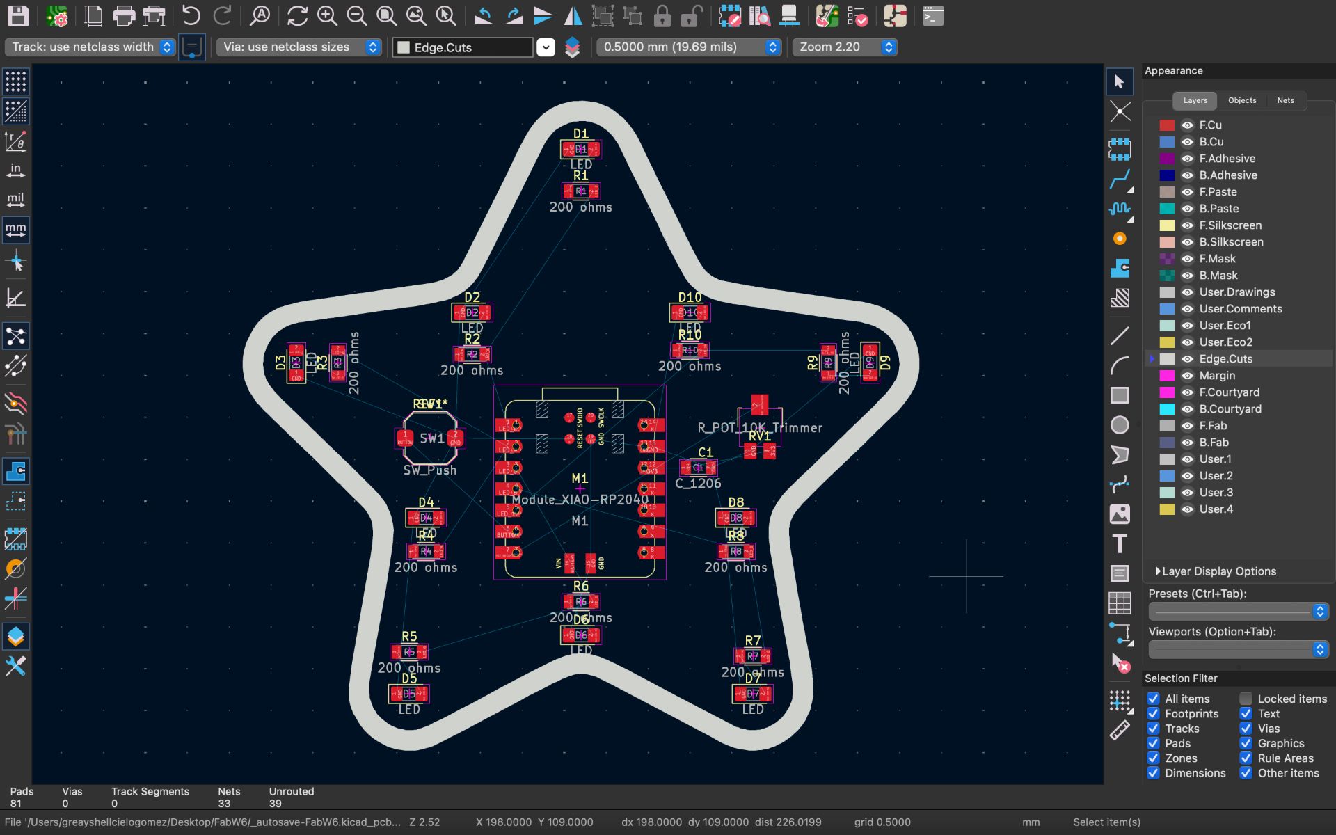
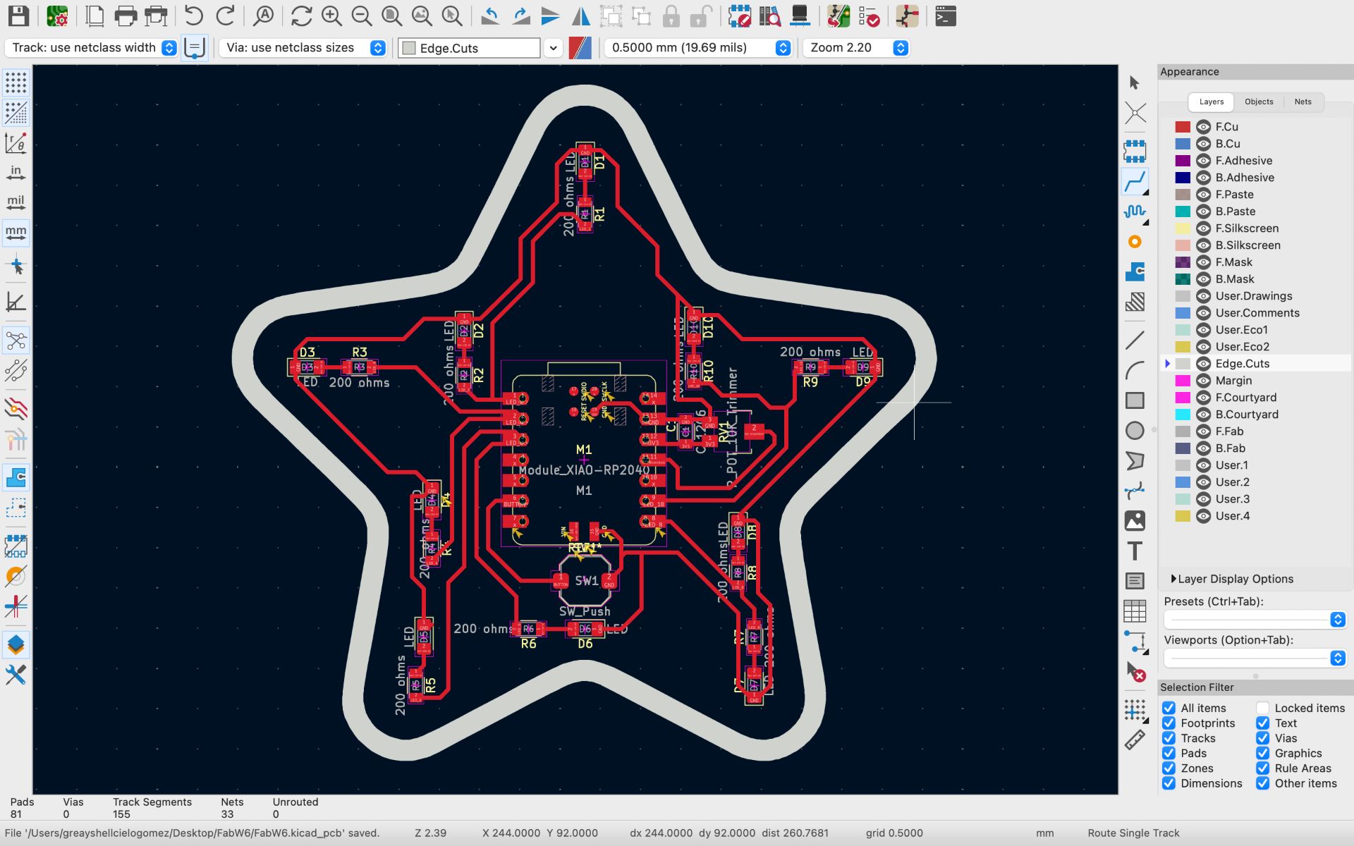
09. FINAL PCB DESIGN
This is the final design of my PCB.
❮
❯
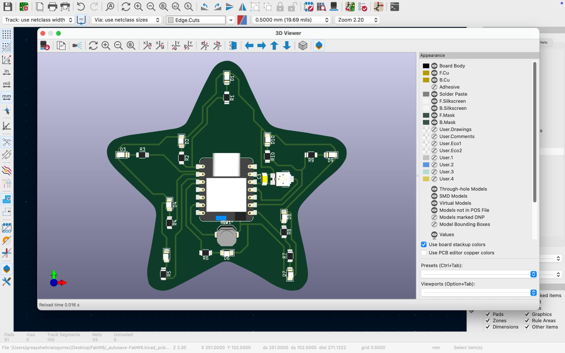
✦ 3D Visualization
To visualize the final PCB design, I went to View → 3D Viewer, which opened a new window displaying the board in 3D. This allowed me to verify the physical placement of the XIAO RP2040 and the rest of the components on the PCB.
✦ Files
In this section, you can find the downloadable source files developed during this week.