Input Devices
Input devices refer to every type of component or module that can receive analogue or digital measurements useful for our projects needs. As simple as it sounds, it is a world of possibilities, as these types of input devices can measure:
- Speed
- Sound
- Atmospheric Pressure
- Altitude
- Motor Position (encoders)
- Touch
- Proximity
- Material Bending
- Etc.
There is most likely a way to input any value you desire to your micro-controller, to process it and act upon it. Learning how the most common input devices work is a useful maker skill that will make you think about your projects in terms of systems that accomplish tasks and, together, solve a problematic.
For more information on how input devices work, check out Lab’s Group Assignemt Page. From this page I learned the big difference between analogue and digital signals. Input devices can come in either form, and it is important to undertand how to work with each type of signal in order to expand our input devices repertoire.
Component vs Modules
There are two main ways of using input devices: components vs modules.
On one hand, a component refers to a single electrical component that serves as an input device by itself or with the help of a few extra controllers. These components are the purest way of implementing input devices into your project, as you are in charge of designing your PCBs and scripts to accommodate the component. This is a double edge sword, as some components requiere multiple extra components to work properly, harder to make wiring or complex soldering processes.
Components give you control in exchange of convenience.
On the other hand, a module refers to a pre built PCB with the components necessary for an out-the-box input capability. Its just like using component based inputs devices, but someone already designed and assembled the PCB for you. Modules are the easy, already proven way of implementing input devices into your project. The one big downside to modules are that they are already built, meaning that your project’s PCB must accommodate the device, not the other way around. Plus, modules tend to be a little bit more expensive that the component alone.
Modules give you convenience in exchange of control.
Which One to Use?
As most thing, it depends on your personal cases. For simple, single-component input devices, using the component itself can be even easier than using a module, as the module will most likely be more expensive, bulkier and with “unnecessary” components.
For more complex input devices, like encoders or buck converters, using a module might be more desired. This input devices tend to be more complex in their functionality, leaving a bigger error margin for beginner makers trying to design and solder it. Plus, these modules are already tested, meaning that you can rest assured that, once in your project, they will work as intended.
Testing an Input Device
For my project, I need an array of microphones to input speech into a Speech-To-Text library for my TLM (Tiny Language Model) to receive prompts), but also as a way of finding the overall direction of the sound to trigger its rotating base to face it. For this, 4 microphones might be enough.
The recommended microphone type for this type of application would be a MEMS (Micro Electrical Mechanical System) microphone. A MEMS microphone is a tiny electrical component that, with a small diaphragm inside of it, reproduces the sound received into either an analog or digital signal for our program to read.
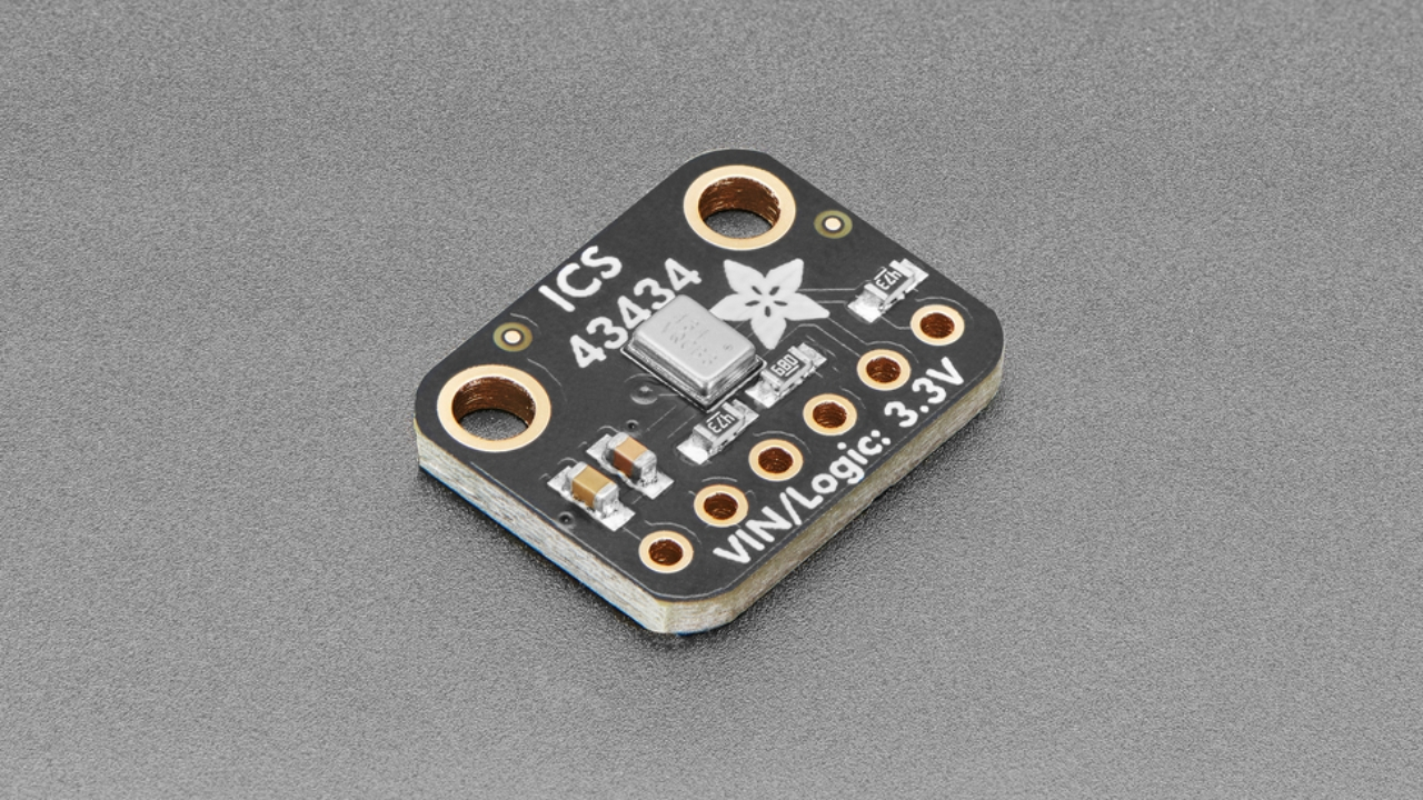
For our specific use case, a digital signal will allow us to get a better quality audio for the Speech-To-Text to process it and return us a prompt. For this reason, using a module like the Adafruit ICS 43434 is an amazing choice. The module comes in a small sized PCB with the corresponding pads to solder or wire into our existing PCB. These modules are also cheap, which is great for our use case because we will be needing at least 4. And most importantly, using the module saves us time and effort, as the MEMS microphone is really small and its soldering pads are too close together for a single layer PCB like the ones we have access to produce.
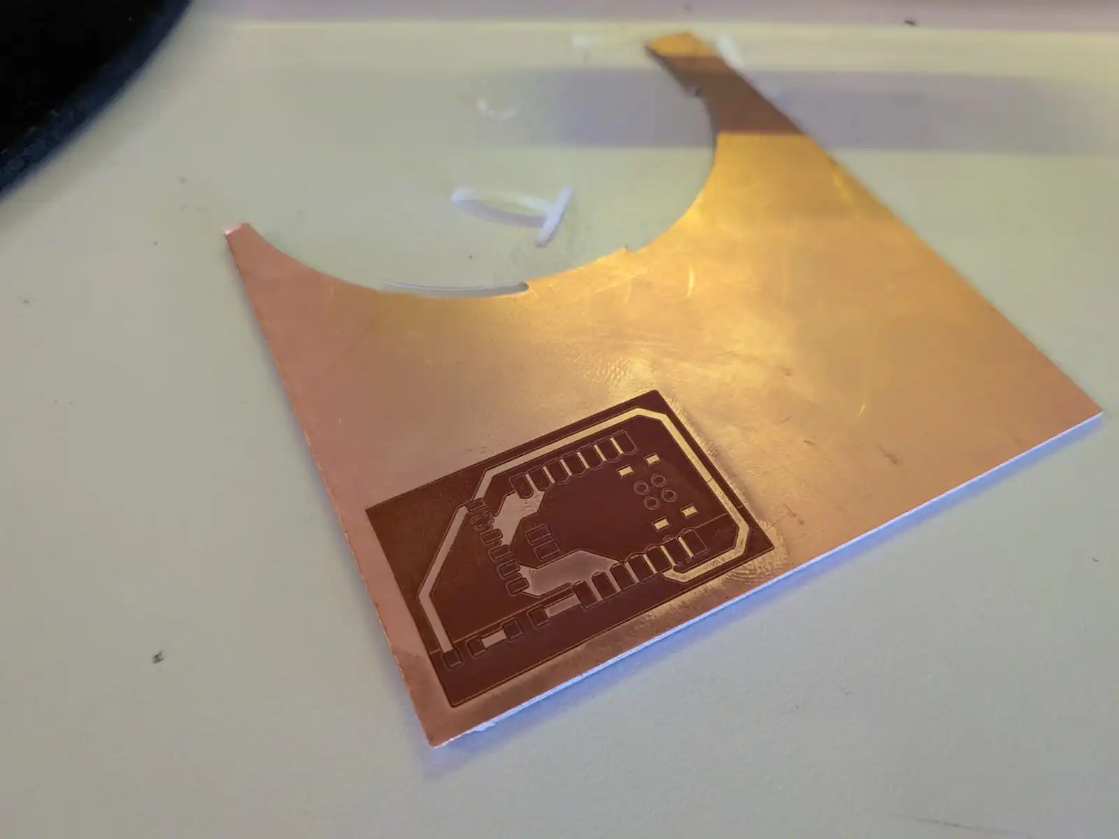
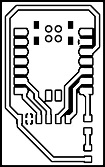
Designing the PCB
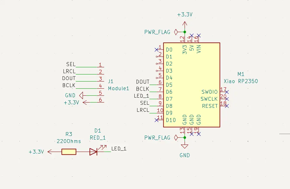
Our PCB for this microphone will be really simple: It will have a Xiao RP2350, an LED that will signal noise detection, and 6 pads corresponding to the 6 pads needed for the module.
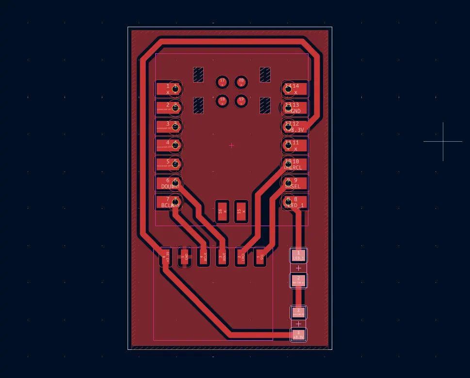
Then, we create the PCB layout. Again, this process is quite easy considering the few amount of components and the simplicity of its connections:
Now, we simply export the Gerber file and, using FabLab Kerela‘s Gerber to PNG, we get our PNG file to upload.

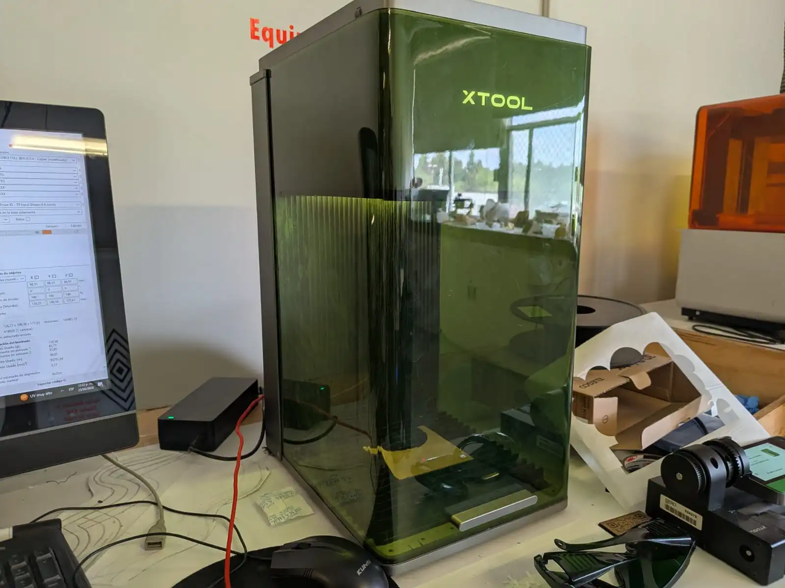
XTool F1 Ultra
Last week I had no time to use the XTool F1 Ultra for PCB production, and now I have an opportunity to do it. Ever since I saw the XTool potential, I was eager to try it out. Unlike the Roland milling machine, the XTool uses laser to engrave and even cut the PCB itself. Personally, it feels like a more “profesional” tool for PCB production, specially for small PCBs like this one.
Operating the XTool F1 Ultra is relatively easy, you can take a look the previous week Lab group assignment page for a more detailed guide on how to prepare your XTool F1 Ultra.
Assuming your XTool is already calibrated, following the group assignment instructions, we first need to import our SVG or PNG image into a new workspace.
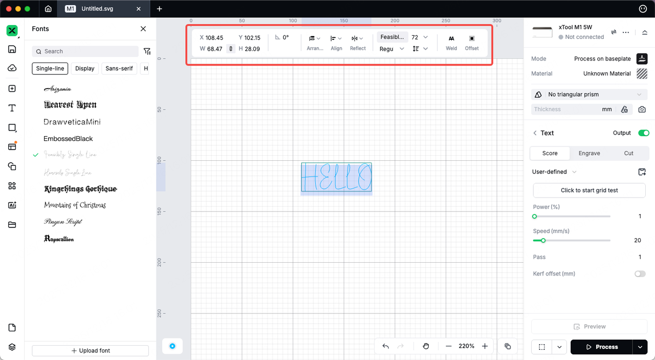
Now, we must configure the parameters for the laser cutter. For this first trial we used the following parameters, taken directly from the series of tests made in the group assignment page. These parameters are:
- Job type: Engrave.
- Laser type: IR Fiber.
- Power (%): 100.
- Speed (mm/s): 750.
- Passes: 10.
- Lines per cm: 300.
- Engraving mode: Unidirectional.
These parameters where meant to be enough to engrave the PCB in a single job. Now, its time to send the file into the XTool itself. For this, we just need to click the Engrave button underneath the laser configuration. A window will appear with the Job preview and a Start button on the right-top corner of the Screen.
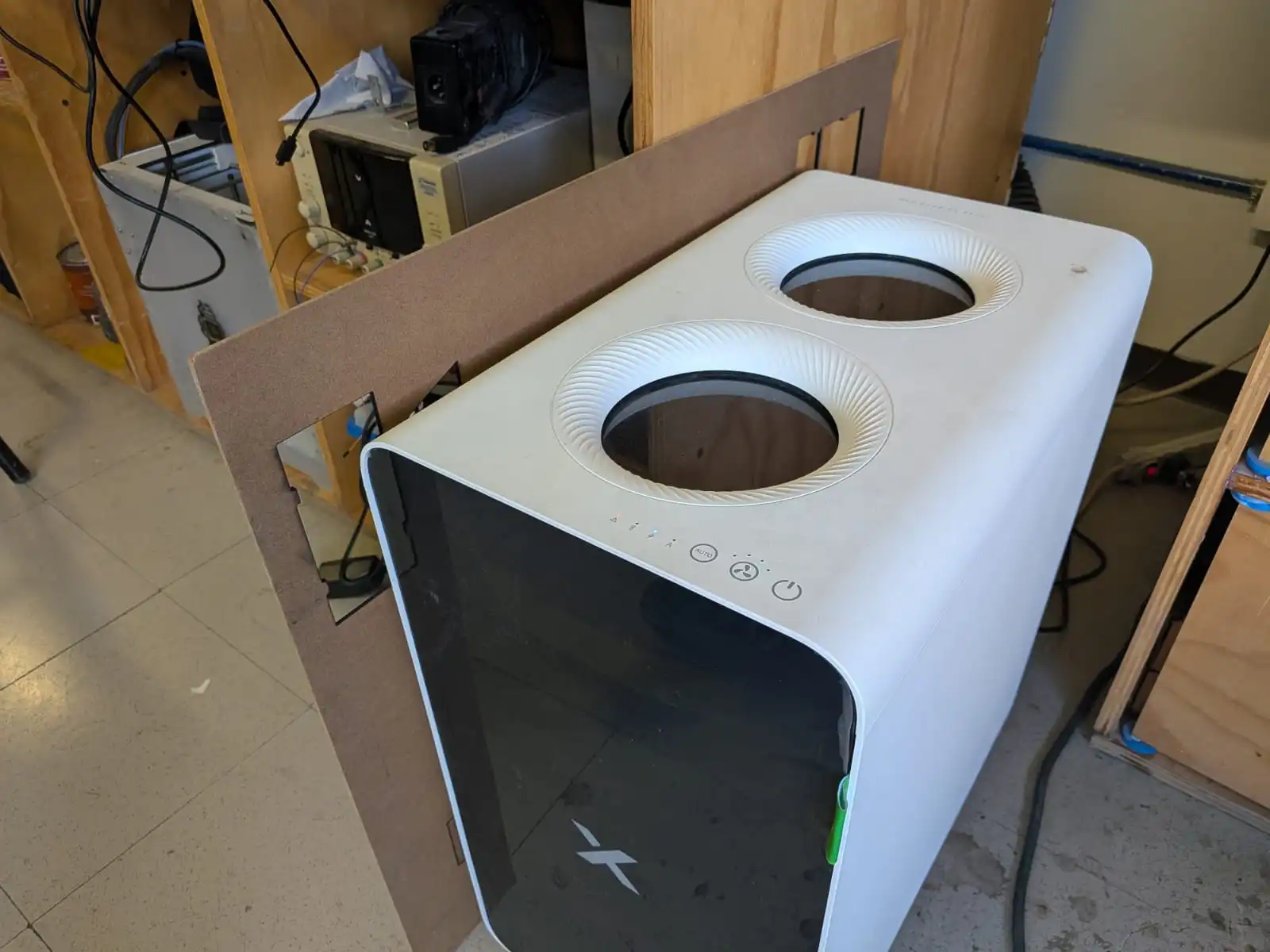
Now its time to prepare our material, by placing it into the XTool chamber. We can use a little bit of tape to secure it into the base, although I didn’t find this step as necessary as with the Roland. Now, we must lower the chamber protection screen.
Make sure the XTool extraction unit is on and working correctly, as fumes may be released during the job.
With the extraction unit ready and the chamber closed, we can go into our XTool control panel (the screen with the big green button) and press it. The laser will start working automatically! Make sure to stay near the laser cutter at all times in case something goes wrong.
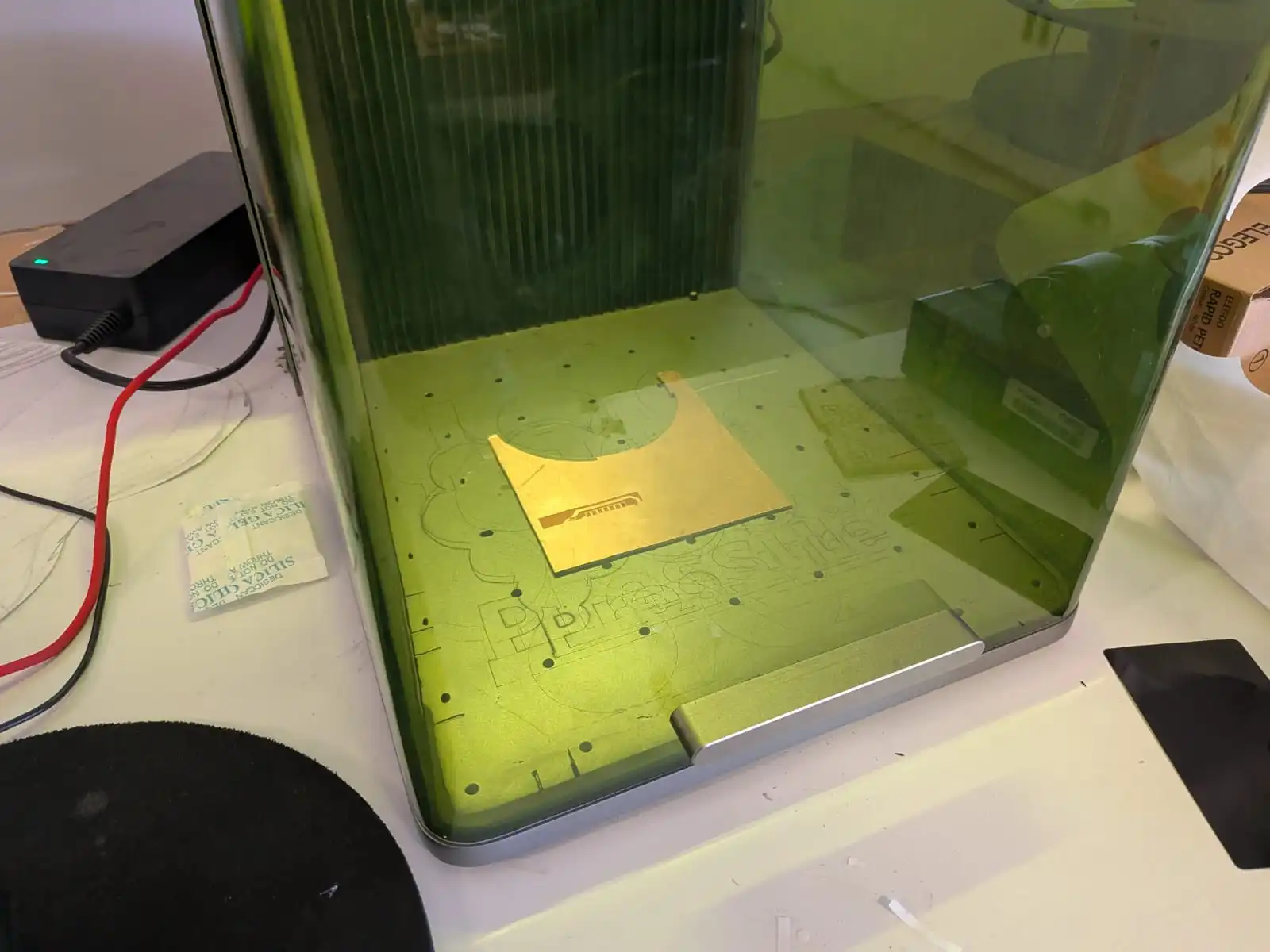
Your screen will show the time remaining for the job to be done. When the job is over, wait a few seconds for the extraction unit to completely remove any fumes that might have been generated during the engraving process. Now, simply open the chamber and remove your material.
First Engraving Analysis
Our first engrave, as expected, wasn’t completely successful. For starters, the laser interpreted our SVG wrong. The white areas where meant to be engraved, and the black areas where meant to stay as copper. This first engraving mixed up the colors, engraving the black areas and preserving the white areas. The second problem was continuity. When testing the PCB engraved areas and the copper layer with a multimeter, there was continuity between both sections, meaning the PCB wasn’t fully engraved yet.
Second Attempt
For this second attempt I firstly inverted the colors of my PCB images, so that the XTool would engrave the correct sections.
Now, it was time to modify my initial parameters. For this second attempt I decided to follow the advice of a fellow Ibero Puebla FabLab student, Leonardo Batista. He was able to not only engrave, but also cut his PCB, all in the XTool F1 Ultra. I used his last set of parameters:
- Job type: Engrave.
- Laser type: IR Fiber.
- Power (%): 100.
- Speed (mm/s): 1000.
- Passes: 10+.
- Lines per cm: 300.
- Engraving mode: Unidirectional.\
- Material Thickness: (the PCB thickness).
Leonardo explains that his previous attempts failed because the material thickness wasn’t properly configured. He also explains that multiple passes might be required to complete the engraving process. I asume that doing 10 passes, then another 10 and so on is ideal to get a perfect Engraving.
Following his advice (thanks Leonardo), I did a second attempt. This time, the results where more promising, although not perfect.
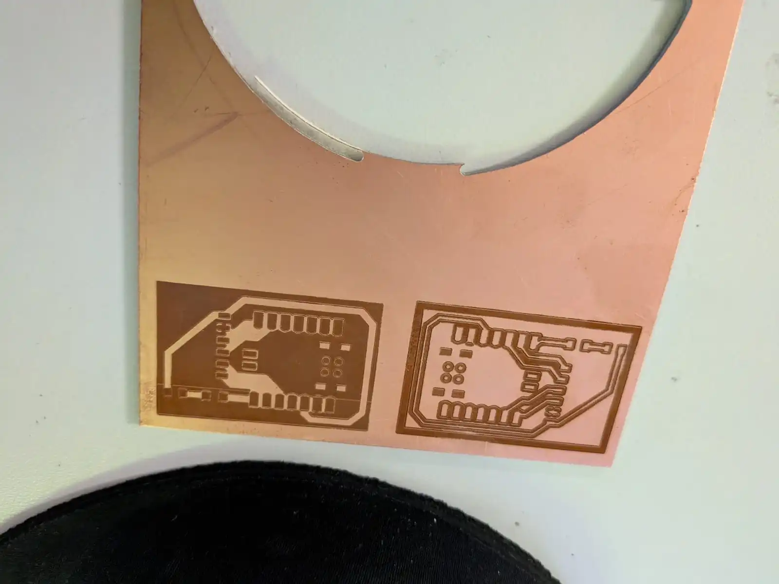
This second attempt (the one on the right) is now engraved correctly but not enough. When testing the board with a multimeter, continuity was still present between the engraved and non-engraved areas of the PCB. This means that the engraving process did not fully removed the copper layer.
As Leonardo’s page said, multiple passes where needed, so I tried with another 5 passes, and then another 5 passes. Results stayed the same.
Trial and Error
Given that I was the only student using the XTool, I took my time to run my own tests on parameters. I five different configurations:
- The Lab’s Group Assignment parameters.
- Leonardo Batista’s parameters.
- ChatGPT generated parameters (not as serious as the other ones).
- Daniel Tartaglia YouTube video parameters.
- JTMakestl YouTube video parameters.
The main difference between these parameters where the speed (mm/s) and cuts per cm. JTMakestl parameters did actually went through the copper layer, but severely burnt the lower layers. The rest resulted into similar engravings, all without correctly engraving the PCB.
After this series of test, I came to the conclusion that speed (mm/s) was the most important parameter to get right. A high speed resulted into a beautifully engraved PCB but without removing the copper layer. An extra low speed resulted into removing the copper layer in one job, but burning underneath.
My Personal Best Parameters
My last PCB was a success. Among all the changes made to the parameters, I also used the automatic measurement tool to detect the material thickness. Previously, I measured 1.4mm as my copper plate thickness. The XTool detected a 2.4mm thickness, which checks out with a common tip I saw while investigating the parameters I tested: add +1mm to your material thickness.
Plus, there was a hidden configuration I also added to the parameters: The cross pattern option, under the advanced configurations menu.
With this in mind, I ended up doing 3 different jobs:
| Power % | Speed (mm/s) | Passes | Lines per cm | Frequency | Progressive Angle | Cross Pattern | |
|---|---|---|---|---|---|---|---|
| Engraving Job | 100 | 600 | 10 | 240 | 32 | Yes | Yes |
| Cleaning Job | 100 | 750 | 5 | 240 | 32 | Yes | Yes |
| Finishing Job | 80 | 1400 | 1 | 240 | 45 | Yes | Yes |
The whole PCB production took some time (1+ hour). But, in the end, the results where worth the wait. In my hands where the best PCB I’ve ever produced. Every track had a perfect resolution, even the smallest ones reserved for connecting ground pads to the ground plane. The area between the tracks was smooth, without messy protruding material.
The resulting PCB was perfect. Almost perfect…
Side Quest: Cutting my PCB
I was so exited with my results that I forgot I never cut the PCB layout previous to the engraving process, which meant that my PCB was stuck inside the whole copper plate. Leonardo Batista was able to cut his PCB with the XTool itself, but I wasn’t ready to spend more time testing for parameters to do a job that, being honest, is not meant to be done with the XTool. For future PCBs, cutting the layout first in the Roland machine seems like a great idea.
Now, I needed figure how to remove my PCB from the copper plate. Using a Dremel tool seemed like a good choice, but every instructor I consulted gave me the same answer: using a Band Saw.
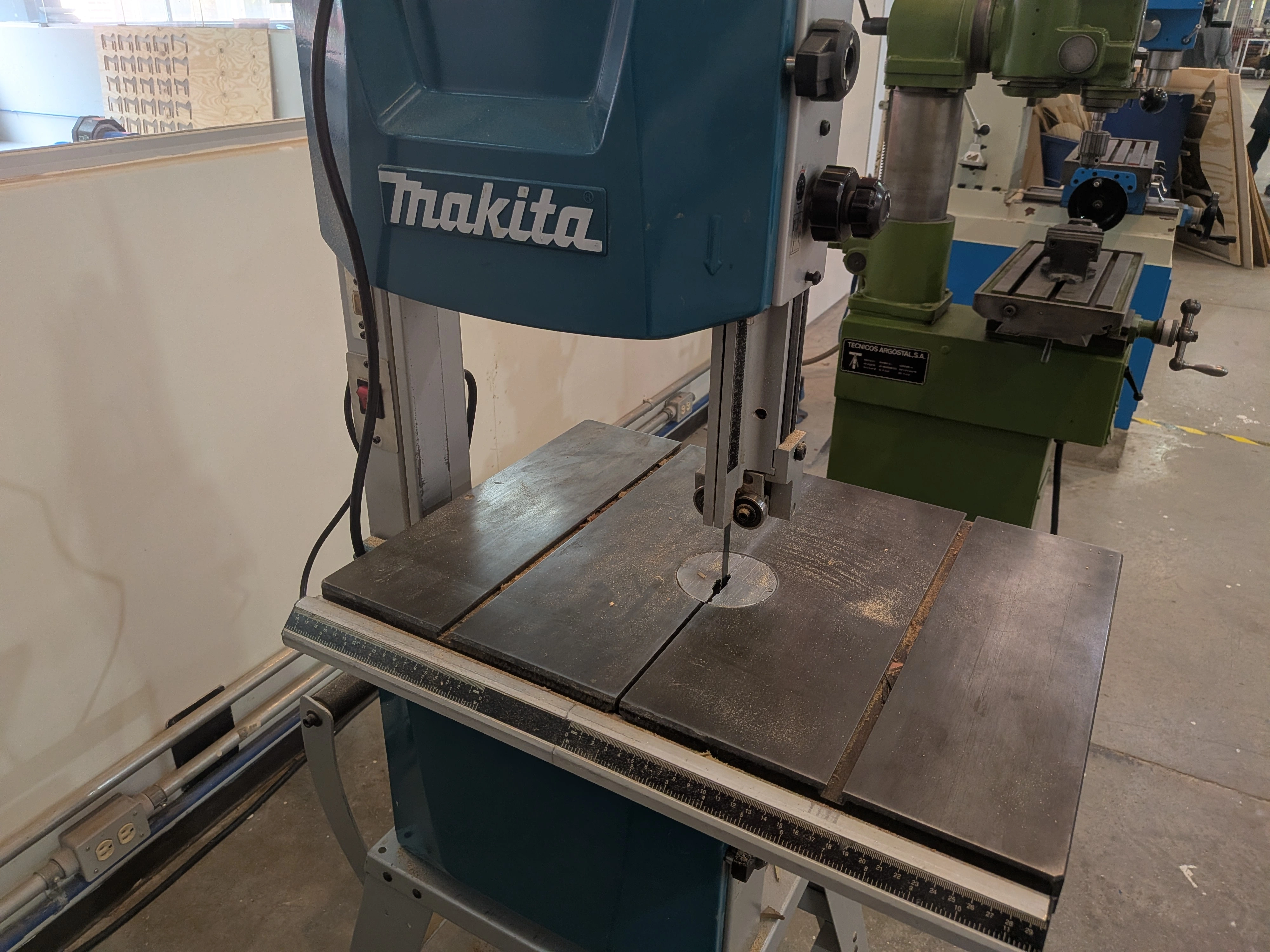
My university has a lot of tools at our disposal, one of them being a band saw. So, I had to use a band saw for the first time. Using a band saw is quite straight forward: You just need to insert your material through the moving band following your layout. It is not as dangerous as it might seem, but there are a few considerations you must keep in mind before using a band saw:
- Always use glasses.
- Hold your material tightly with your hands with enough separation between your fingers and the band.
- Material might fly with speed if it is separated from the base material with a cut from the band saw. To prevent this, remove from the band saw when only a sliver of material is holding the piece, then remove by hand.
With these precautions in mind, we can start cutting the PCB. There is no video of this process, as I was alone, but it went surprisingly smoothly for my first time.
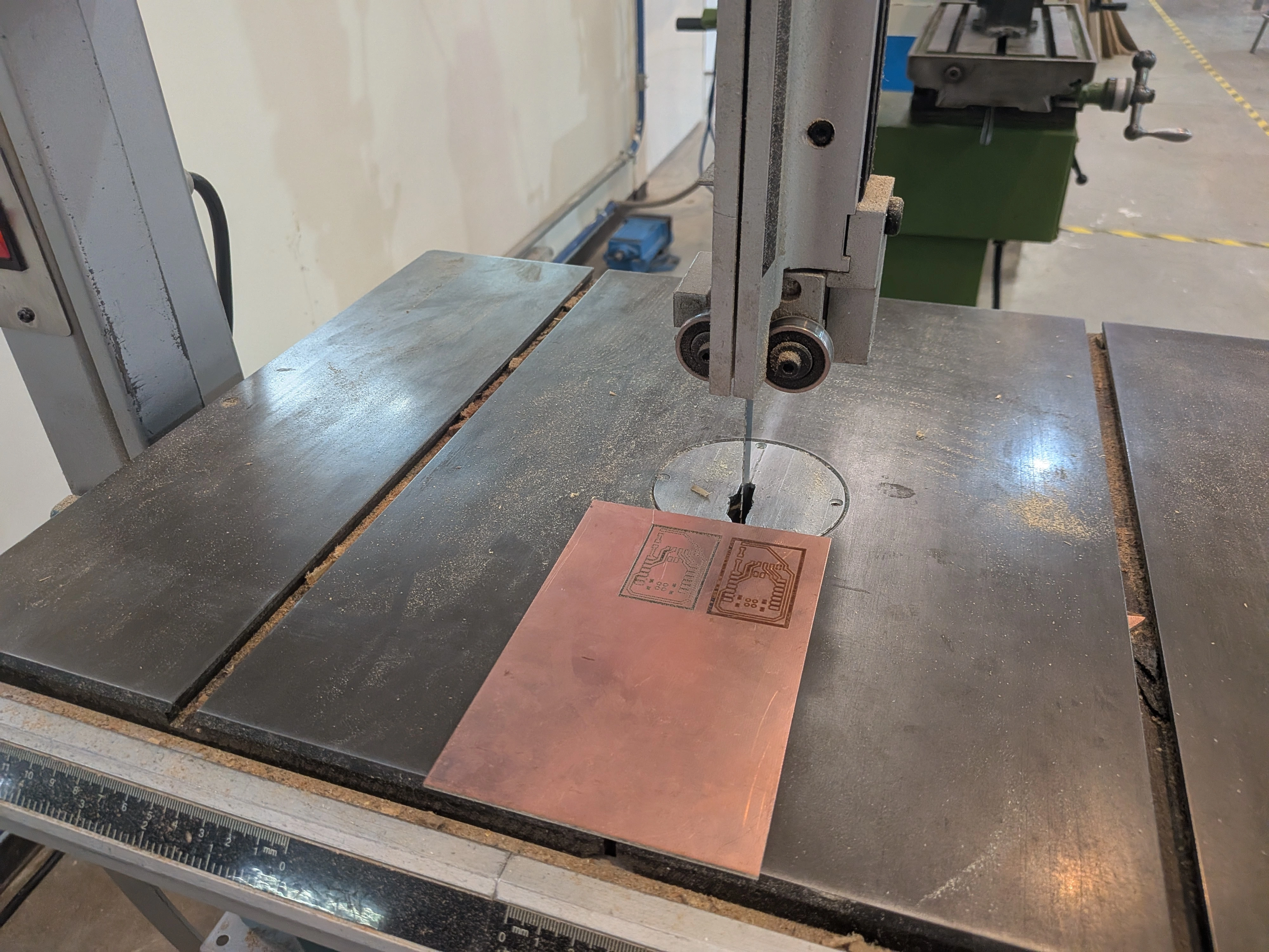
After using the band saw, the PCB was ready!
Testing the Microphone
Note: From now on, we’ll be using an INMP441 mems microphone module. Plus, our micro-controller will be a Xiao esp32s3 (more on that later).
Using a MEMS microphone can be as easy or as hard, depending on what we want to accomplish with it. I initially wanted to recreate a “wake up word” functionality, brought to us directly from Espressif with their ESP-SR library. This library comes prebuilt with some speech commands, such as “Hey, ESP!” in order to trigger custom functionalities in our code. ESP-SR would come really in handy for my final project, as it requires a wake up word to start our process, as seen in my [user diagram], in my final project page.
Here’s the problem. At least for me, working with ESP-SR was a nightmare. There is little to no documentation on how to implement it into our main IDEs: Arduino IDE and VSCode + Platformio. Arduino IDE 2 doesn’t include the ESP-SR library directly. This means that including the necessary imports for ESP-SR into our scripts is basically imposible. The alternative was VSCode + Platformio, where we have the most control over our project structure.
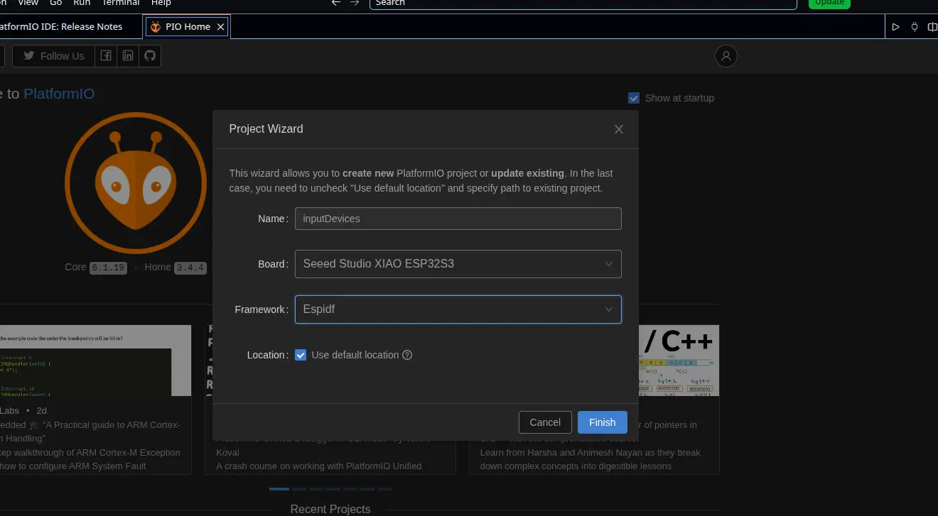
Trying Platformio
I searched up on YouTube and Google examples or guides on how to include the ESP-SR library on to a Platformio project, as the ESP-SR repo I linked to above does not have an installation guide. The only thing I did knew I had to do was changing my development framework from Arduino to ESPIDF (ESP IoT Development Framework), as this (in theory) should have given me a better experience, given that both ESPIDF and ESP-SR come directly from Espressif.
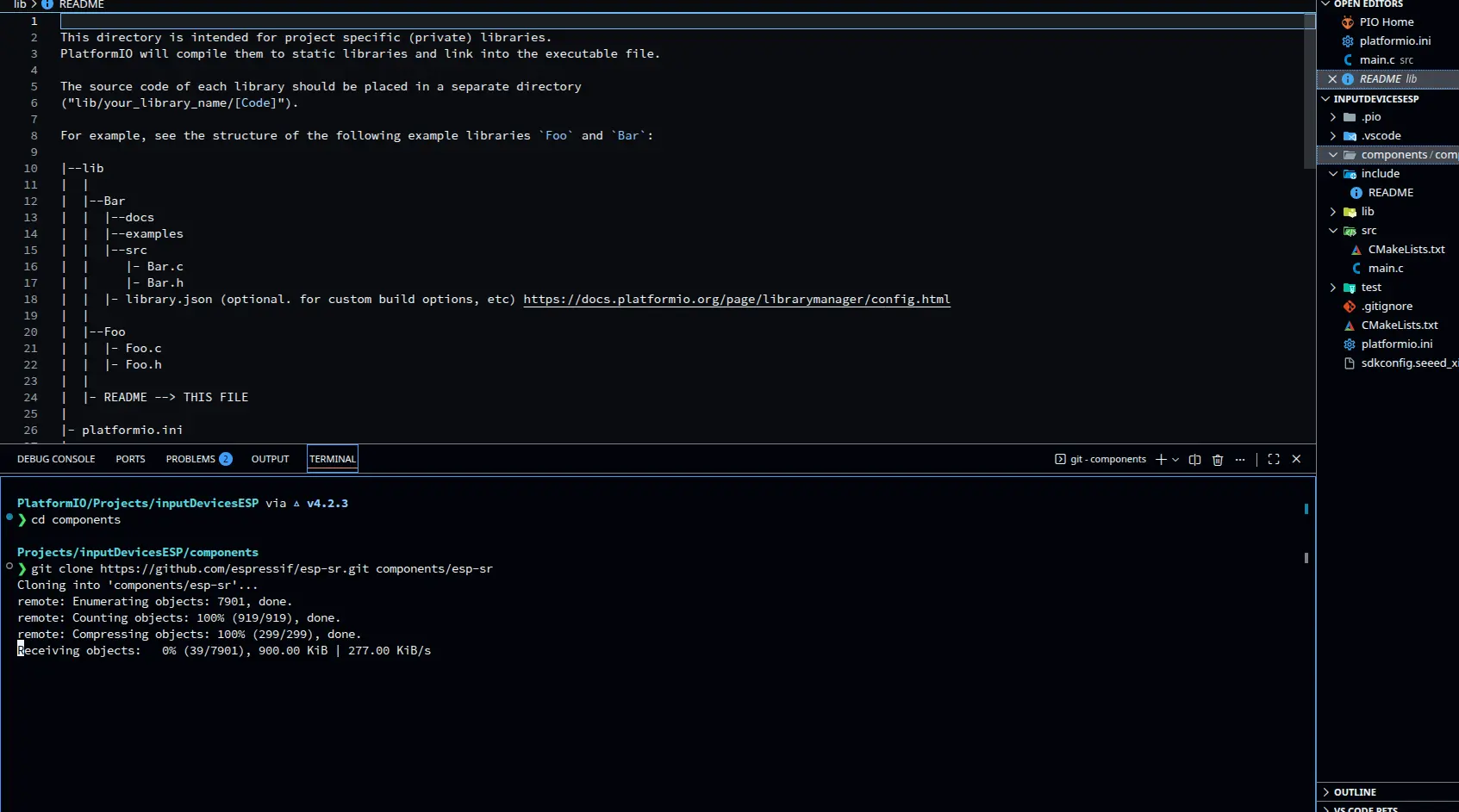
The next step I figured out, with some AI assisted research, was cloning the ESP-SR repo into our project, in a new directory called “components”. Apparently, Platformio reads the contents of “components” as external libraries for us to import into our main script. So, I created the directory, moved into it and ran gh repo clone espressif/esp-sr to clone the repo. This command might not work for you, assuming you have not installed the GitHub CLI Tools like me. I you don’t, run git clone https://github.com/espressif/esp-sr.git instead.
Now, using an AI generated Script, thanks to Claude AI (script can be found under the Files section of this page), I tried to compile it into my micro-controller: a Xiao esp32s3. The decision of using an esp32s3 instead of a RP2350, for example, was for a better implementation of the ESP-SR library, built for esp32s3 chips.
Running Into Issues
The importation of the necessary libraries to run ESP-SR given by our AI agent were not being detected. Here’s where the lack of available information really hindered our process. I had no idea into what was causing the issue, as it could really be anything. My AI agent tried debugging the problem by making me change my platformio.ini and multiple CMake files, but nothing. I tried manually changing the importation routes of the libraries in my main.c file to better fit the library location in my project, but nothing. The more I tried debugging the more problems I faced.
Reflection: AI Can Be Wrong
I want to take a moment to reflect on how AI is not a “magic” problem solver. As I said before, there are not a lot of tutorials and guides (not that I could find) on how to implement ESP-SR into either Arduino ide or Platformio. If I have no available information online, neither does an AI agent. Here’s the problem: Generative AI’s, like Claude AI, MUST answer with something. This phenomenon is usually called “hallucinations”, where an AI, trying to comply to its “always answer with something” nature, returns information that might look like a valid answer, but in reality it is not. At first glance, everything that the AI told me to do seemed like a valid way to solve my problem. The further we went though, it became more apparent that neither the AI or I had a clue on what was causing the problem.
The main takeaway of the situation is to use AI as a tool, not as a problem solver. Understanding how AI works will also help you understand that it has its limitations. AI is a powerful tool that most can really benefit from, but a knife by itself is useless if not in the hands of an expert chef. We sometimes fall into the trap of letting AI do the whole work. Maybe for some simple tasks this is a valid strategy, and a good use of AI if I may. But for more complex tasks, call it ESP-SR debugging or Software development, where background knowledge is a must: AI is “useless” without knowledge on what you are doing and what you want to accomplish.
So, use AI. Get the most out of it. But understand that AI by itself can not do anything. But you, you can.
And please, document your projects properly.
Plan B: Simple Sound Sensor
I ditched the wake up word script (at least for now). Now I was only interested on getting my INMP441 module to detect sound. Just that. Luckily for me, the instructions on how to do this are more clearly than with ESP-SR. The idea is to use I2S, a sound transmitting protocol, to connect the INMP441 to my Xiao esp32s3, in order to receive values from it.
I guided my self from this INMP441 I2S Guide. This page had everything I needed to get my INMP441 microphone to work, from connection tables to a basic Arduino code to run. My final script was based on this Arduino code with some modifications:
- Added a threshold for the sound values (thanks to AI recommendation) .
- Added a serial plotter output to better visualize the information.
The resulting script looks like this:
#include <driver/i2s.h>

        #define I2S_WS 7
        #define I2S_SCK 8
        #define I2S_SD 44

        #define I2S_PORT I2S_NUM_0
        #define SAMPLE_RATE 16000
        #define BUFFER_SIZE 1024
        #define SILENCE_THRESHOLD 500

        int32_t buffer[BUFFER_SIZE];

        void setup() {
        	Serial.begin(115200);
        	delay(1000);

        	i2s_config_t i2s_config = {
        		.mode = (i2s_mode_t)(I2S_MODE_MASTER | I2S_MODE_RX),
        		.sample_rate = SAMPLE_RATE,
        		.bits_per_sample = I2S_BITS_PER_SAMPLE_32BIT,
        		.channel_format = I2S_CHANNEL_FMT_ONLY_LEFT,
        		.communication_format = I2S_COMM_FORMAT_STAND_I2S,
        		.intr_alloc_flags = ESP_INTR_FLAG_LEVEL1,
        		.dma_buf_count = 8,
        		.dma_buf_len = BUFFER_SIZE,
        		.use_apll = false,
        		.tx_desc_auto_clear = false,
        		.fixed_mclk = 0
        	};

        	i2s_pin_config_t pin_config = {
        		.bck_io_num = I2S_SCK,
        		.ws_io_num = I2S_WS,
        		.data_out_num = I2S_PIN_NO_CHANGE,
        		.data_in_num = I2S_SD
        	};

        	i2s_driver_install(I2S_PORT, &i2s_config, 0, NULL);
        	i2s_set_pin(I2S_PORT, &pin_config);
        	i2s_zero_dma_buffer(I2S_PORT);
        }

        void loop() {
        	size_t bytes_read = 0;

        	i2s_read(I2S_PORT, buffer, sizeof(buffer), &bytes_read, portMAX_DELAY);

        	int samples_read = bytes_read / sizeof(int32_t);
        	int32_t max_amplitude = 0;
        	int64_t sum_squares = 0;

        	for (int i = 0; i < samples_read; i++) {
        		int32_t sample = buffer[i] >> 14;
        		int32_t abs_sample = abs(sample);

        		if (abs_sample > max_amplitude) {
        			max_amplitude = abs_sample;
        		}

        		sum_squares += (int64_t)sample * sample;
        	}

        	int32_t rms = (int32_t)sqrt((double)sum_squares / samples_read);

        	Serial.print("Max_Amplitude:");
        	Serial.print(max_amplitude);
        	Serial.print("\t");
        	Serial.print("RMS:");
        	Serial.print(rms);
        	Serial.print("\t");
        	Serial.print("Threshold:");
        	Serial.println(SILENCE_THRESHOLD);
        }
The code looks complicated, but in reality most of it is “template code”, or code that will always look the same no matter the final application. The code is divided into n parts. The first one being the I2S configuration. This part will always look the same:
i2s_config_t i2s_config = {
        		.mode = (i2s_mode_t)(I2S_MODE_MASTER | I2S_MODE_RX),
        		.sample_rate = SAMPLE_RATE,
        		.bits_per_sample = I2S_BITS_PER_SAMPLE_32BIT,
        		.channel_format = I2S_CHANNEL_FMT_ONLY_LEFT,
        		.communication_format = I2S_COMM_FORMAT_STAND_I2S,
        		.intr_alloc_flags = ESP_INTR_FLAG_LEVEL1,
        		.dma_buf_count = 8,
        		.dma_buf_len = BUFFER_SIZE,
        		.use_apll = false,
        		.tx_desc_auto_clear = false,
        		.fixed_mclk = 0
        	};

        	i2s_pin_config_t pin_config = {
        		.bck_io_num = I2S_SCK,
        		.ws_io_num = I2S_WS,
        		.data_out_num = I2S_PIN_NO_CHANGE,
        		.data_in_num = I2S_SD
        	};

        	i2s_driver_install(I2S_PORT, &i2s_config, 0, NULL);
        	i2s_set_pin(I2S_PORT, &pin_config);
        	i2s_zero_dma_buffer(I2S_PORT);
Here, the I2S protocol is initiated with predefined variables in the i2s_config. Then the pin connected from the INMP441 to the esp32s3 are defined in the pin_config. Finally, the I2S protocol is initiated. Now, in the loop section:
size_t bytes_read = 0;
        i2s_read(I2S_PORT, buffer, sizeof(buffer), &bytes_read, portMAX_DELAY);
        int samples_read = bytes_read / sizeof(int32_t);
Here, the microphone reads samples when available, reading how many are 32 bits wide.
int32_t sample = buffer[i] >> 14;
This second part is a normalization of the samples, shifting them by 14 bits. This is donde to work with more manageable data. At last we calculate the max amplitude and the RMS (Root Mean Square) for the serial plotter.
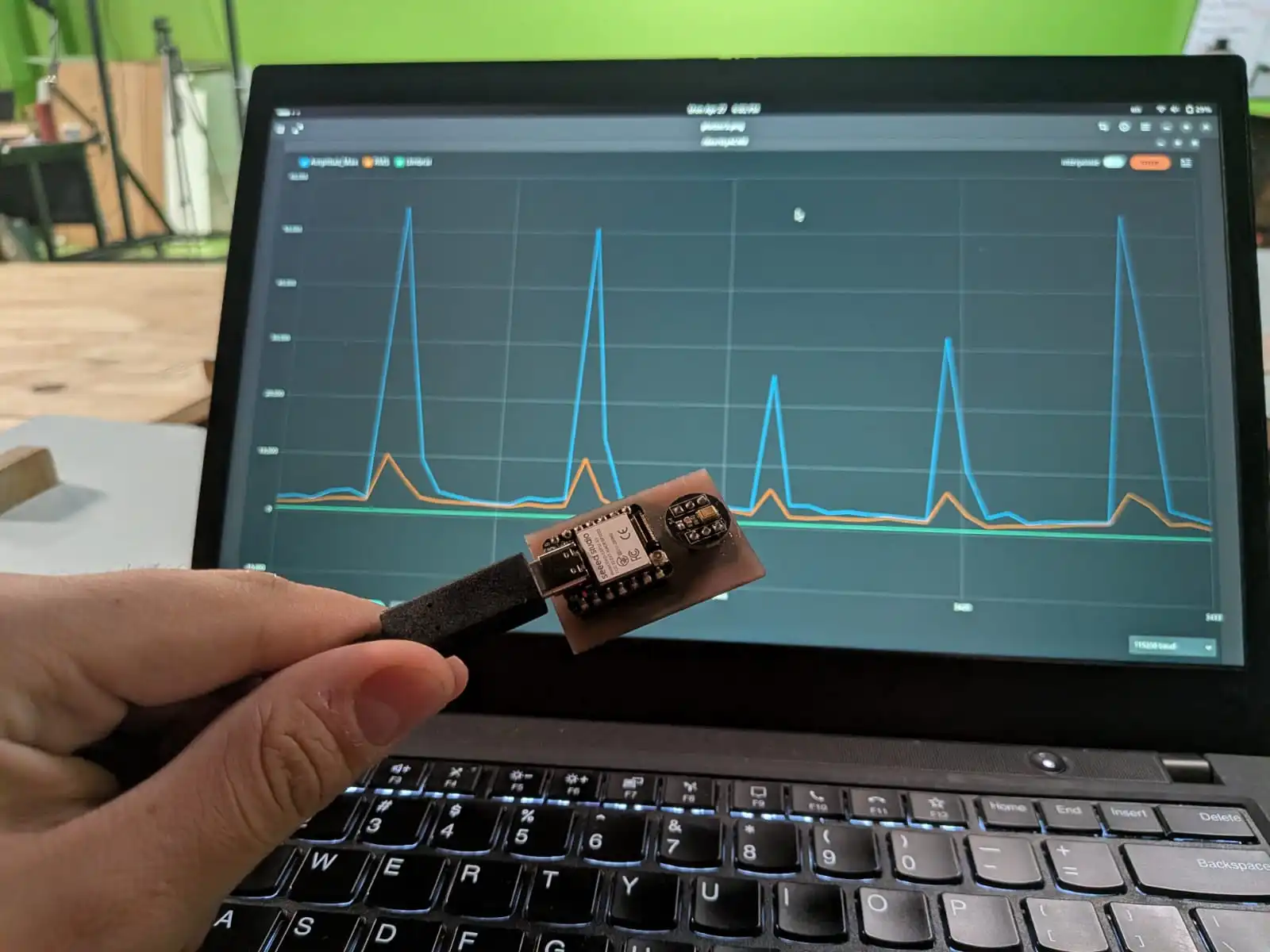
With that, I compiled the script to my esp32s3 and ran the serial plotter:
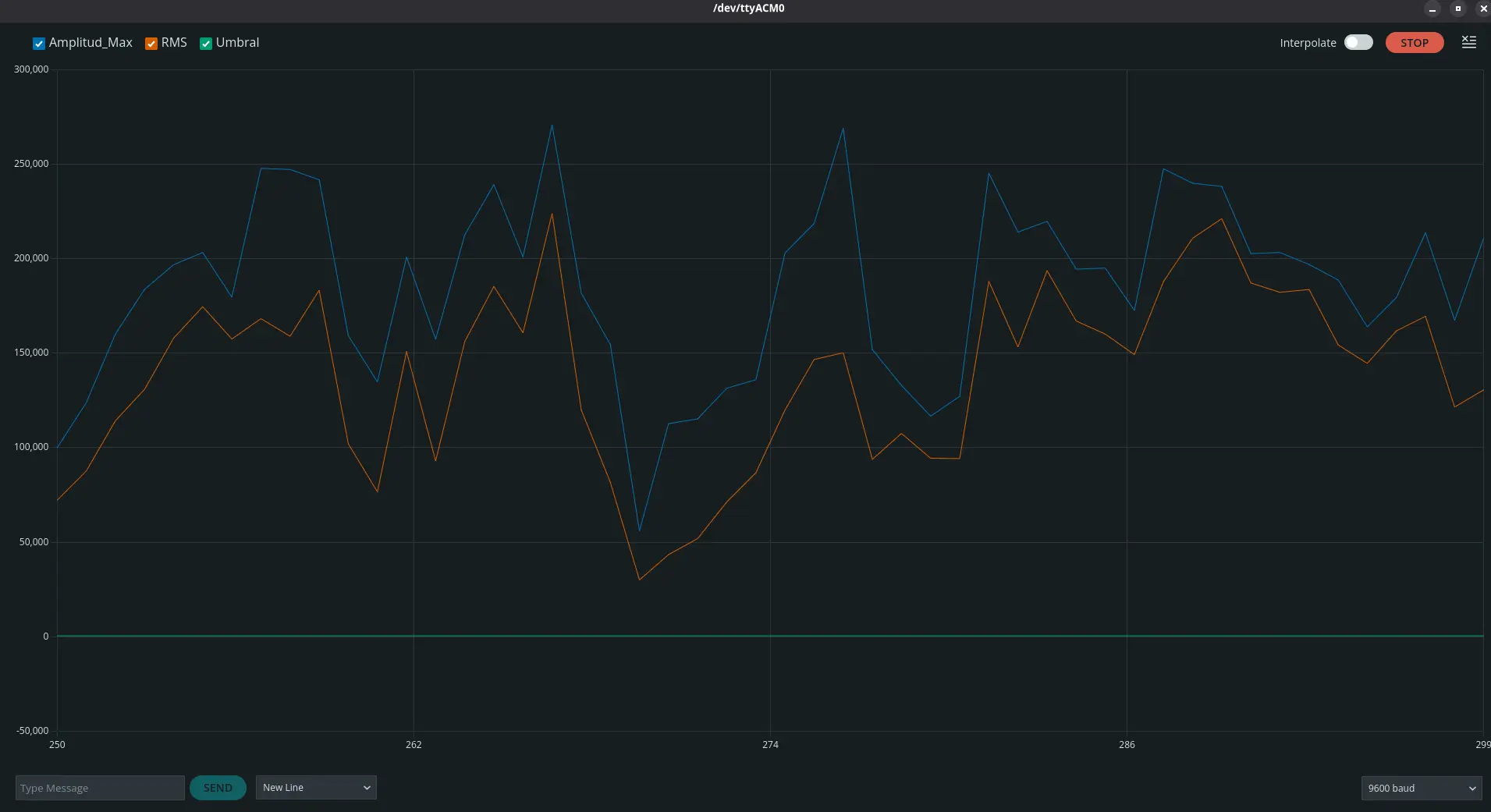
The previous image was the base sound detection in my room with out me making any sound. As we can see, the INMP441 is quite sensitive, capturing the base decibels of my room.
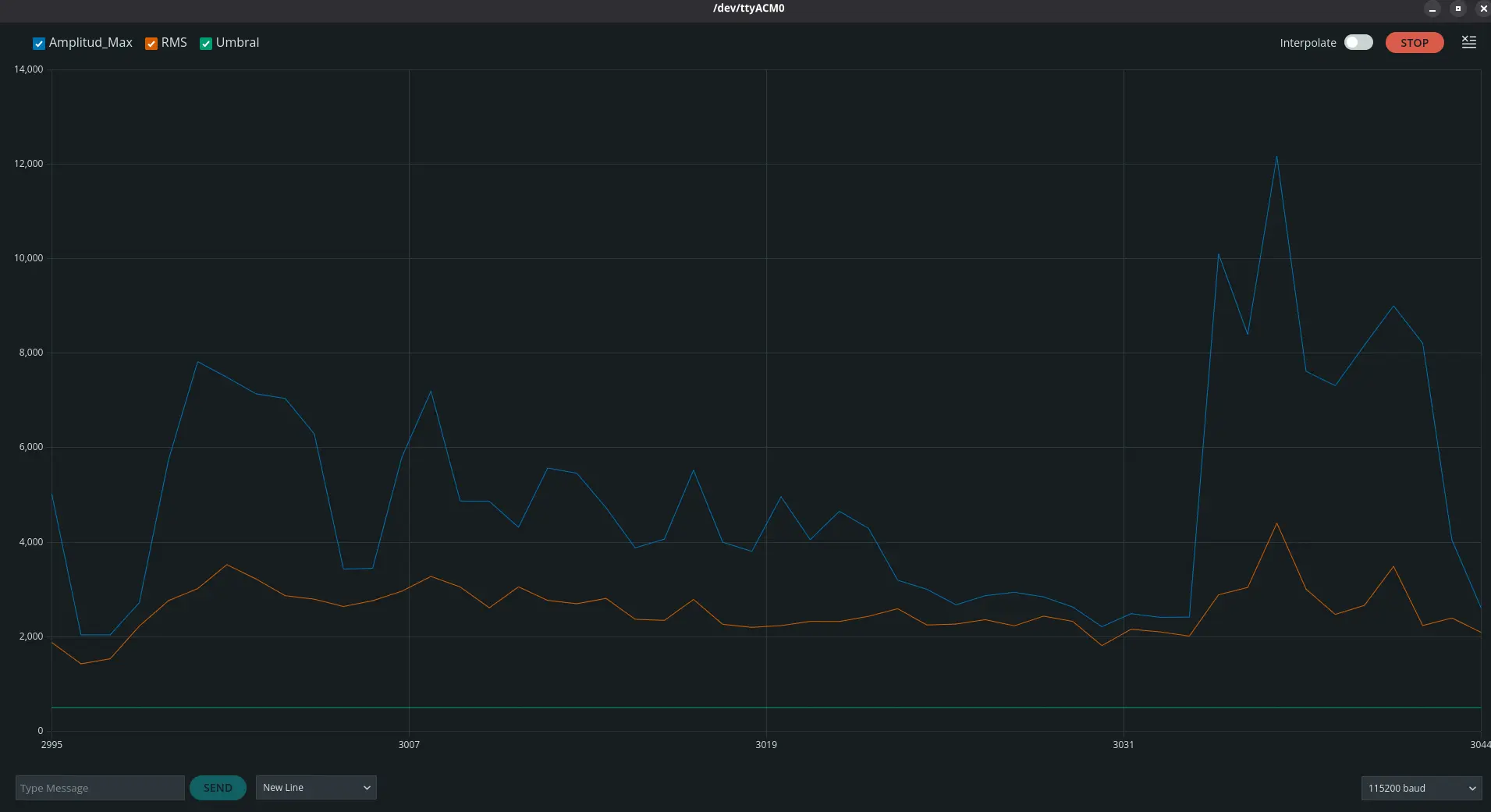
The peek we can observe in this image is me saying the word “Alexa” after a period of silence. As we can see, there is a change on the values captured. The microphone behaved as expected.
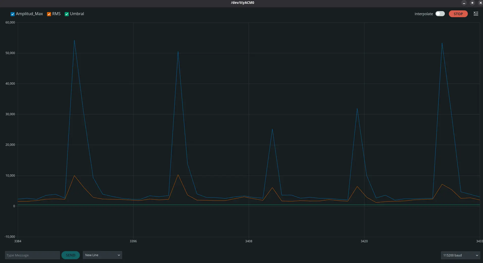
Just for fun, this next image shows me tapping on the microphone. As we can expect, those peeks we can see are the exact moments where I tapped on to the microphone.
The Bottom Line
We might have not been able to accomplish our desired “wake up word” functionality, but we (almost) have a working microphone. Here’s the issue: right now this microphone is only detecting sound as is. For my final project I need it to read speech, in order to run it through a Speech to Text and input it into my LLM as a prompt. Doing this speech detection inside the esp32s3 I am planning on using seems like a hard thing to achieve. But, as I’ll be working with both an esp32s3 and a Raspberry Pi 5, I may be able to use the esp32s3 with the microphone array I’m planning like a dedicated microphone for my Raspberry Pi 5. The Raspberry Pi 5 will then get the speech directly and process both the Speech to Text and wake up word functionalities.
I will be doing more testing on how to convert an INMP441 array into a microphone using the esp32s3 as an intermediary. Who knows, maybe it will be best to link the microphone array directly into the Raspberry Pi 5. Only time and testing will tell. In the mean time, at least we can say I successfully connected a sound sensor into a micro-controller and read its output!