Group assignment
Objective
-
do your lab's safety training
-
Characterize the design rules for your in-house PCB production process: document the settings for your machine.
Document the workflow for sending a PCB to a boardhouse
Here I share the link to my group assignment.
Indivual assignment
What I know
Currently, I have never manufactured a PCB board before. However, I do have experience working with development boards such as the Arduino UNO and the Raspberry Pi Pico, mainly in educational environments with children, using breadboards to build different electronic projects. This will be my first time designing and manufacturing a PCB, so it represents a new learning opportunity and a chance to apply my electronics knowledge to a more advanced design and manufacturing process.
Verifying the Design Created in Week 6
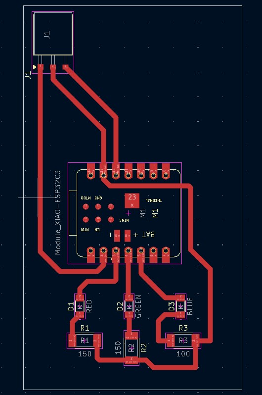
I made several changes to the design developed in week 6. The objective of the circuit is to measure temperature and humidity using the DHT11 sensor. Based on these input values, a LED will turn on depending on the detected temperature. For example, if the temperature is very low the blue LED will turn on; if the temperature is normal the green LED will turn on; and if the temperature is very high the red LED will turn on. The changes I made included modifying the trace width and setting it to 1 mm. I also replaced the THT components with SMD components. To connect the DHT11 sensor, I added header pins. Additionally, I removed the pull-up resistor from the design because the DHT11 module I am using already includes an integrated pull-up resistor.
Previous design
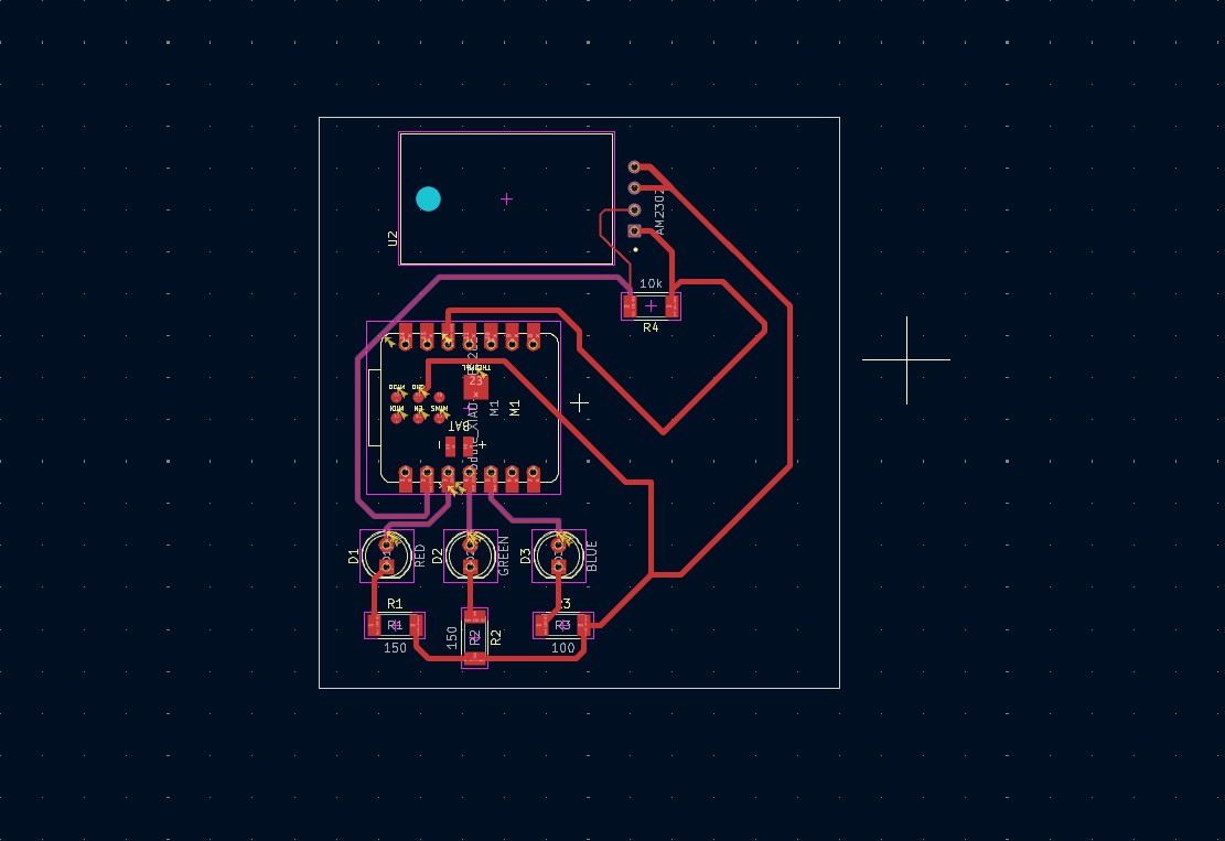
Updated design after making the modifications
Machine used: Xtool F1 Ultra
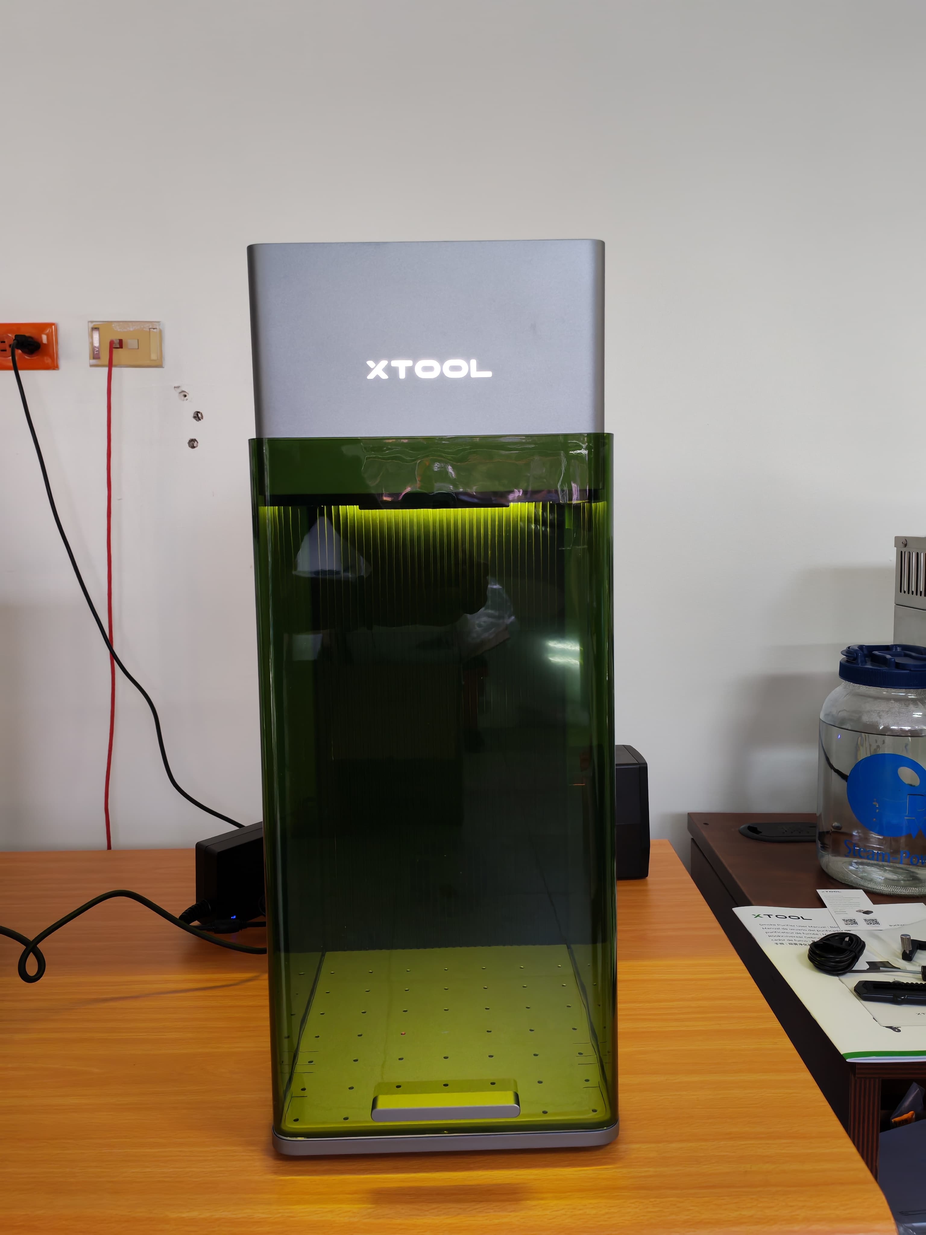
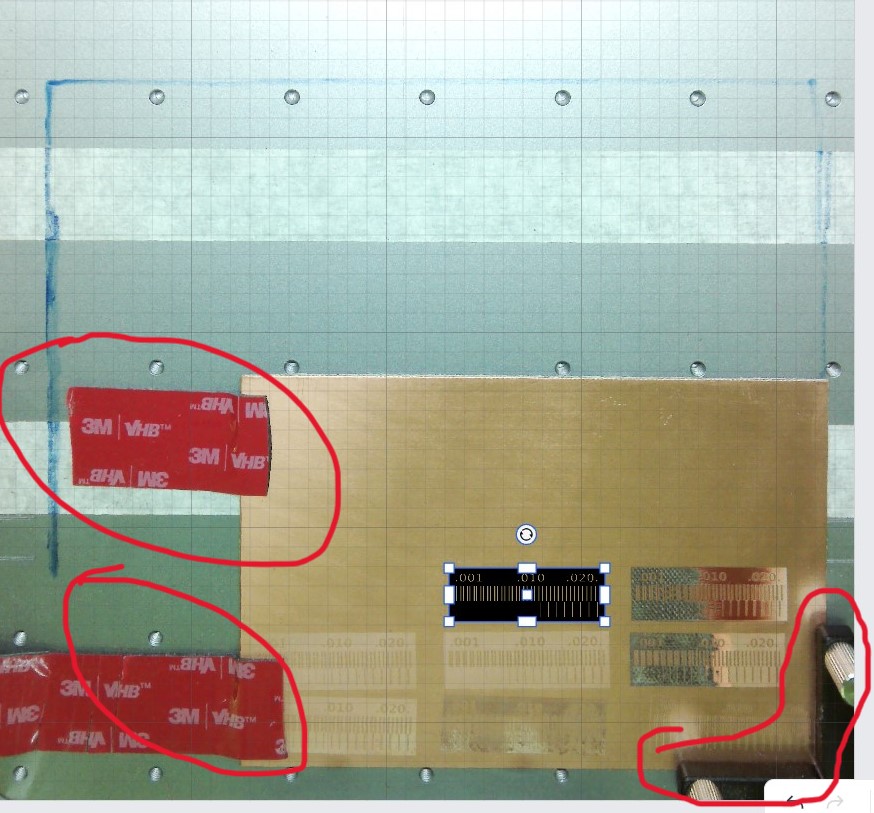
For the fabrication of my PCB board, I decide to manufacture it using the Xtool F1 Ultra. Therefore, I begin by performing some tests. For the first test, I use the following parameters.
Engraving Parameters - Test 1 - xTool F1 Ultra
| Parameter | Value |
|---|---|
| Mode | Flat Processing |
| Process Type | Engraving |
| Laser Type | IR Fiber |
| Power | 100 % |
| Speed | 900 mm/s |
| Pass | 1 |
| Lines per cm | 300 |
| Engraving Mode | Bidirectional |
| Frequency | 30 kHz |
Results of Test 1
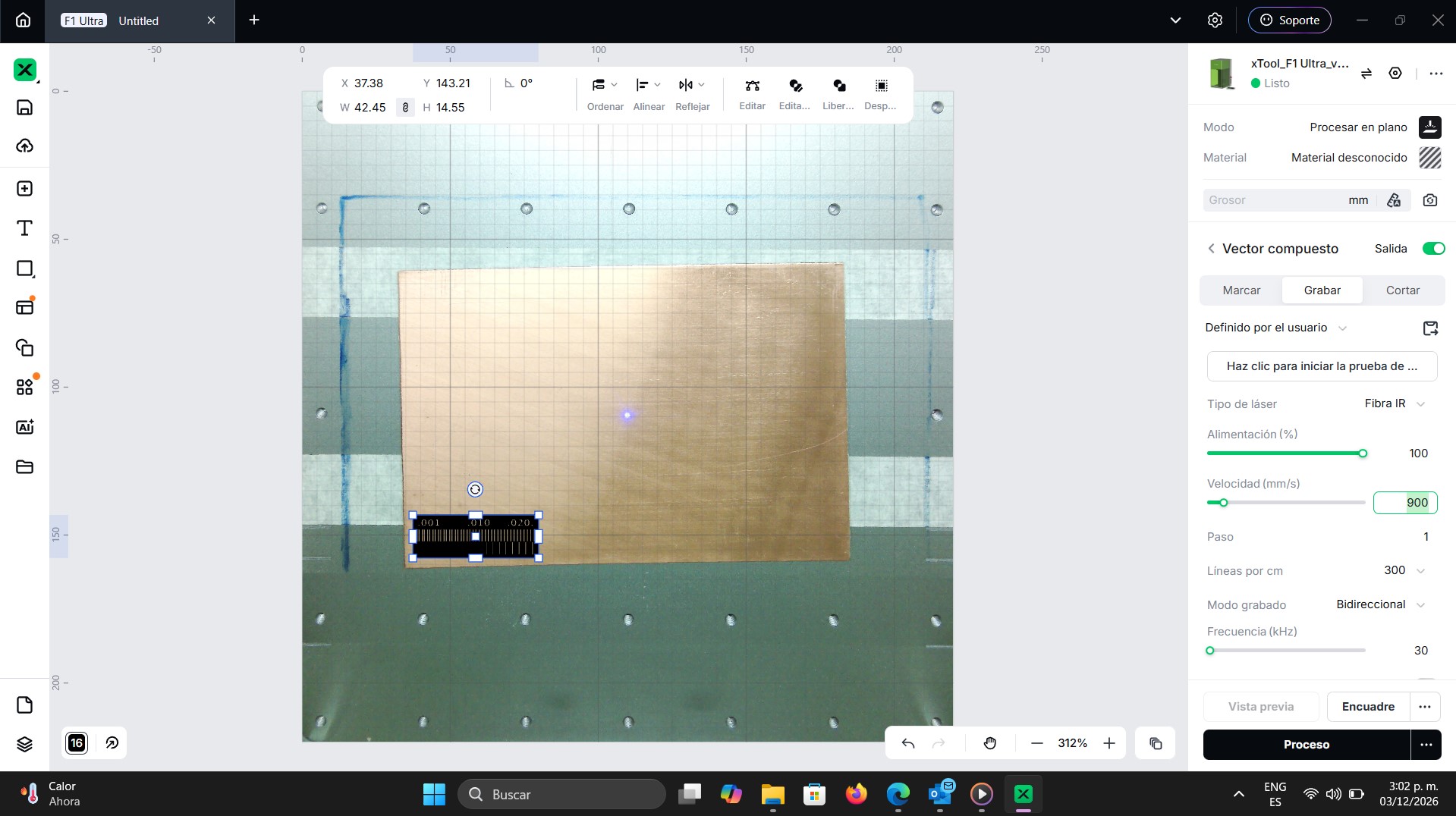
It can be observed that these parameters do not work properly. Even though I am using 100% power, the laser barely affects the copper. For this reason, I decide to perform another test. In this case, I modify the parameters by increasing the number of passes. Instead of one pass, I use 3 passes and reduce the speed to 750 mm/s.
Engraving Parameters - Test 2 - xTool F1 Ultra
| Parameter | Value |
|---|---|
| Mode | Flat Processing |
| Process Type | Engraving |
| Laser Type | IR Fiber |
| Power | 100 % |
| Speed | 750 mm/s |
| Passes | 3 |
| Lines per cm | 300 |
| Engraving Mode | Bidirectional |
| Frequency | 30 kHz |
Results of Test 2
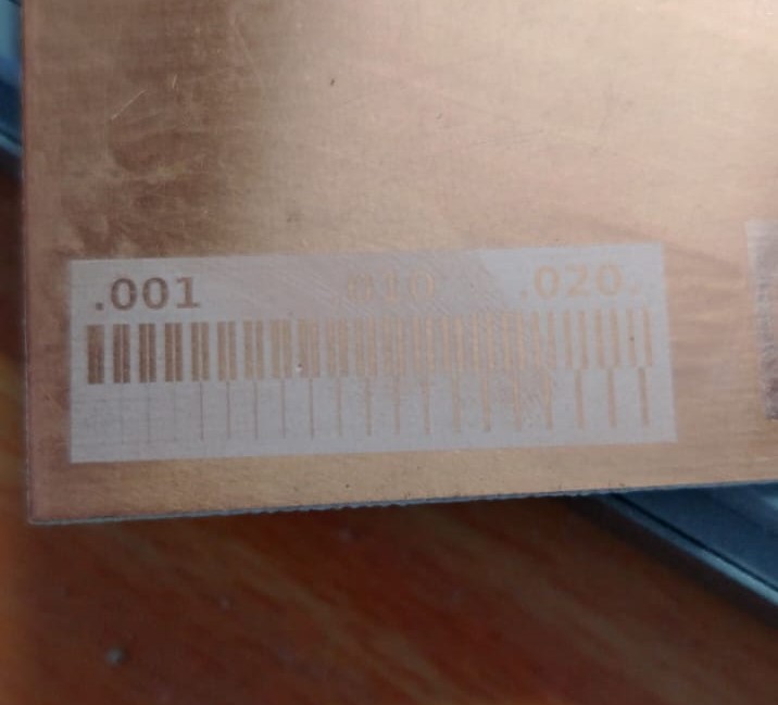
As can be observed, the engraving is still very light and does not improve significantly regardless of the number of passes applied. Due to this situation, I review the parameters again and realize that I had not assigned the material thickness.
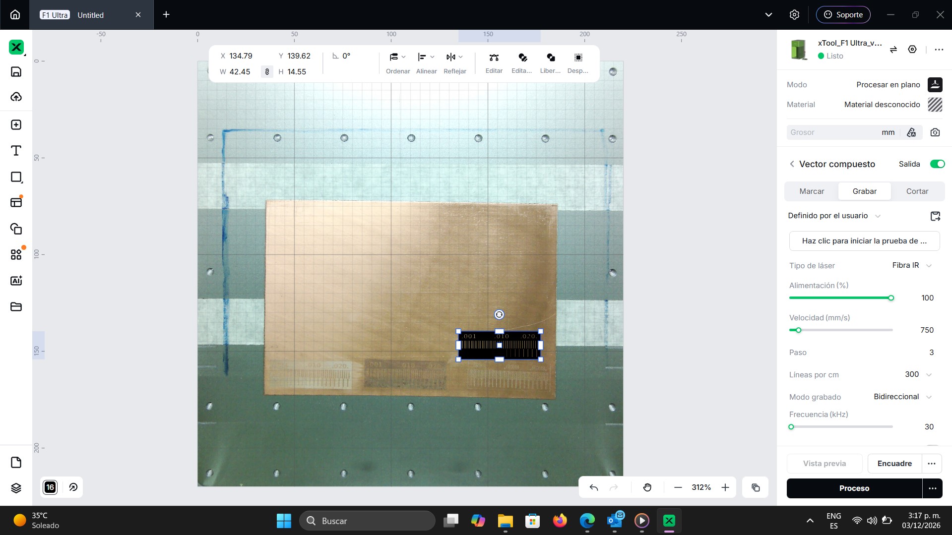
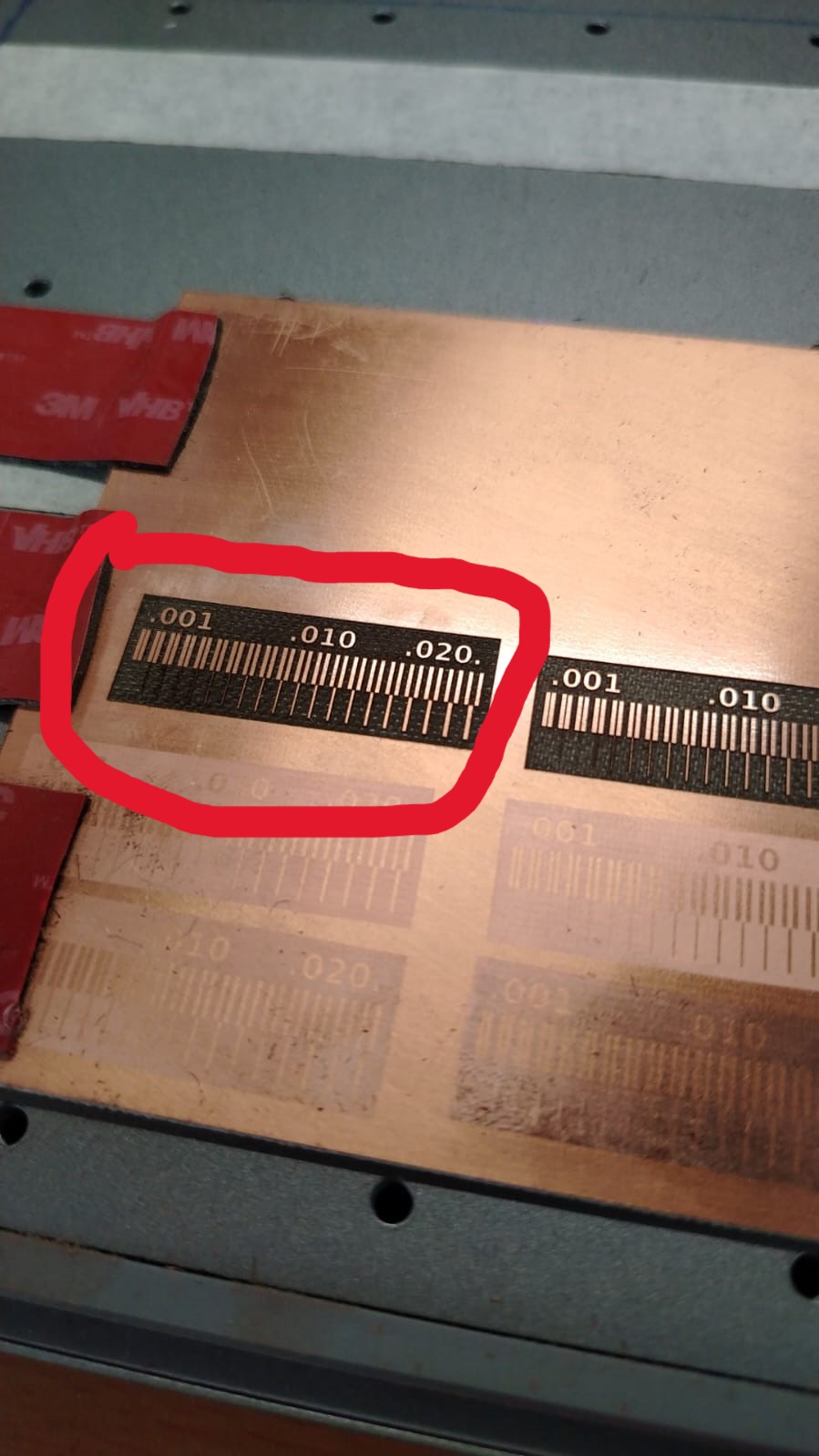
After modifying this parameter, I initially set it to 1.2 mm since the PCB board has that thickness. Using the same previous parameters and only changing the number of passes to 10, I perform another test. This time, a significant improvement in the engraving can be observed. From this test, I conclude that the material thickness was affecting the engraving process. Additionally, the copper board was not perfectly flat, which produced a slight gradient effect in the engraving, as shown in the image.
Engraving Parameters - Test 3 - xTool F1 Ultra
| Parameter | Value |
|---|---|
| Mode | Flat Processing |
| Process Type | Engraving |
| Laser Type | IR Fiber |
| Power | 100 % |
| Speed | 750 mm/s |
| Passes | 10 |
| Lines per cm | 300 |
| Engraving Mode | Bidirectional |
| Frequency | 30 kHz |
| Thickness | 1.2 mm |
To solve this problem, I place the material as straight and flat as possible, as shown below.
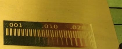
Using the same previous parameters, I perform the engraving again and obtain the following result.
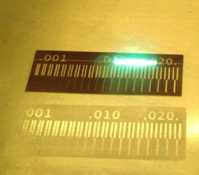
In the image it can be observed that I obtain good results. At this point, I confirm that the material thickness is an important parameter that directly influences the final result. In addition, the material must be as straight and flat as possible in order to maintain a uniform engraving.
I perform one final test, but this time I only change the engraving speed.
Engraving Parameters - Test 4 - xTool F1 Ultra
| Parameter | Value |
|---|---|
| Mode | Flat Processing |
| Process Type | Engraving |
| Laser Type | IR Fiber |
| Power | 100 % |
| Speed | 1000 mm/s |
| Passes | 10 |
| Lines per cm | 300 |
| Engraving Mode | Bidirectional |
| Frequency | 30 kHz |
| Thickness | 1.2 mm |
This was the result.
Conclusion
After performing several engraving tests with the xTool F1 Ultra, I was able to identify the parameters that produce the best results for engraving a copper PCB. Initially, the engraving was very light even when using 100% laser power. After reviewing the parameters, I discovered that the material thickness had not been properly configured, which significantly affected the engraving quality.
Once the thickness was set to 1.2 mm and the number of passes was increased, the engraving quality improved considerably. Additionally, I noticed that the flatness of the copper board plays an important role in achieving uniform engraving results. If the material is not completely flat, the engraving may appear uneven or produce a gradient effect.
Based on these tests, I conclude that the most important factors for achieving a good engraving result are correctly defining the material thickness, using multiple passes, adjusting the engraving speed, and ensuring that the PCB material is as flat as possible.
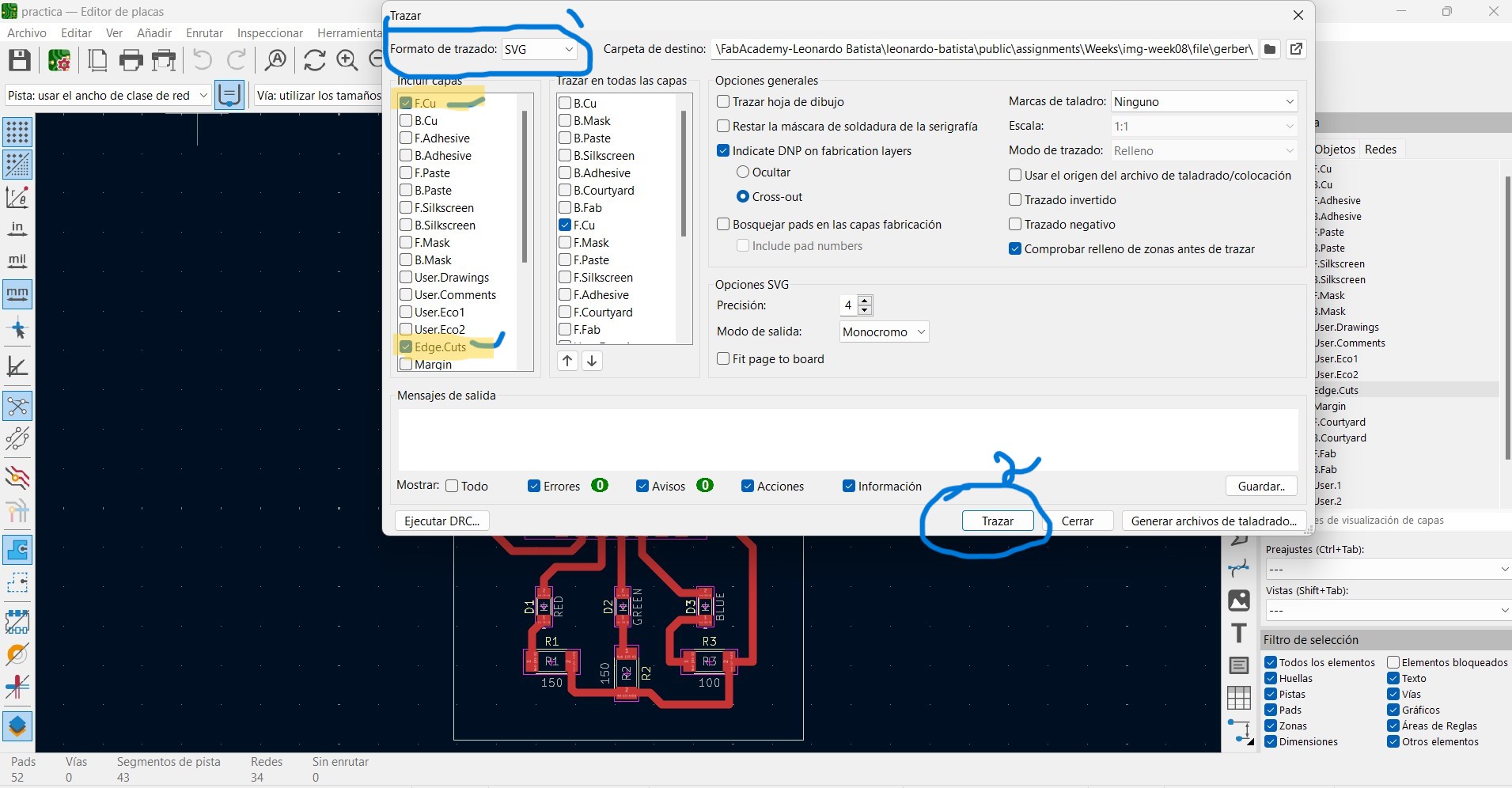
Once these parameters were defined, I was able to start fabricating my PCB. The first step was to export my KiCad design in SVG format.
After exporting the file, I loaded it into the xTool software to send it for engraving. I used the same parameters; however, this time I changed the thickness value from 1.2 mm to 22 mm because I placed the xTool cutting grid under the PCB. The combined height of the grid and the copper board is approximately 22 mm, so I adjusted this value in the settings. Once everything was ready, the engraving process started.
After that, I performed the cutting process using the xTool.
Final result.
At this point it was time to solder the components. However, I must explain that I currently do not have access to SMD components such as surface-mount resistors or capacitors. I checked several electronics stores here in Panama, but they only sell traditional through-hole (THT) components.
Ordering them from another country is not currently a viable option due to logistical limitations. To solve this problem, I started searching through old electronic boards from discarded devices in order to recover usable components.
I managed to recover three resistors: two of 75 ohms and one of 220 ohms. At first I thought I had solved the problem; however, when I placed the resistors and LEDs on my PCB, I realized that they did not match the footprints used in the design. This makes sense because the design was originally made for 1206 resistors and larger LEDs, while the components I found were much smaller and could not be soldered properly.
This situation forces me to modify the PCB design to adapt it to the available components and engrave the PCB again.
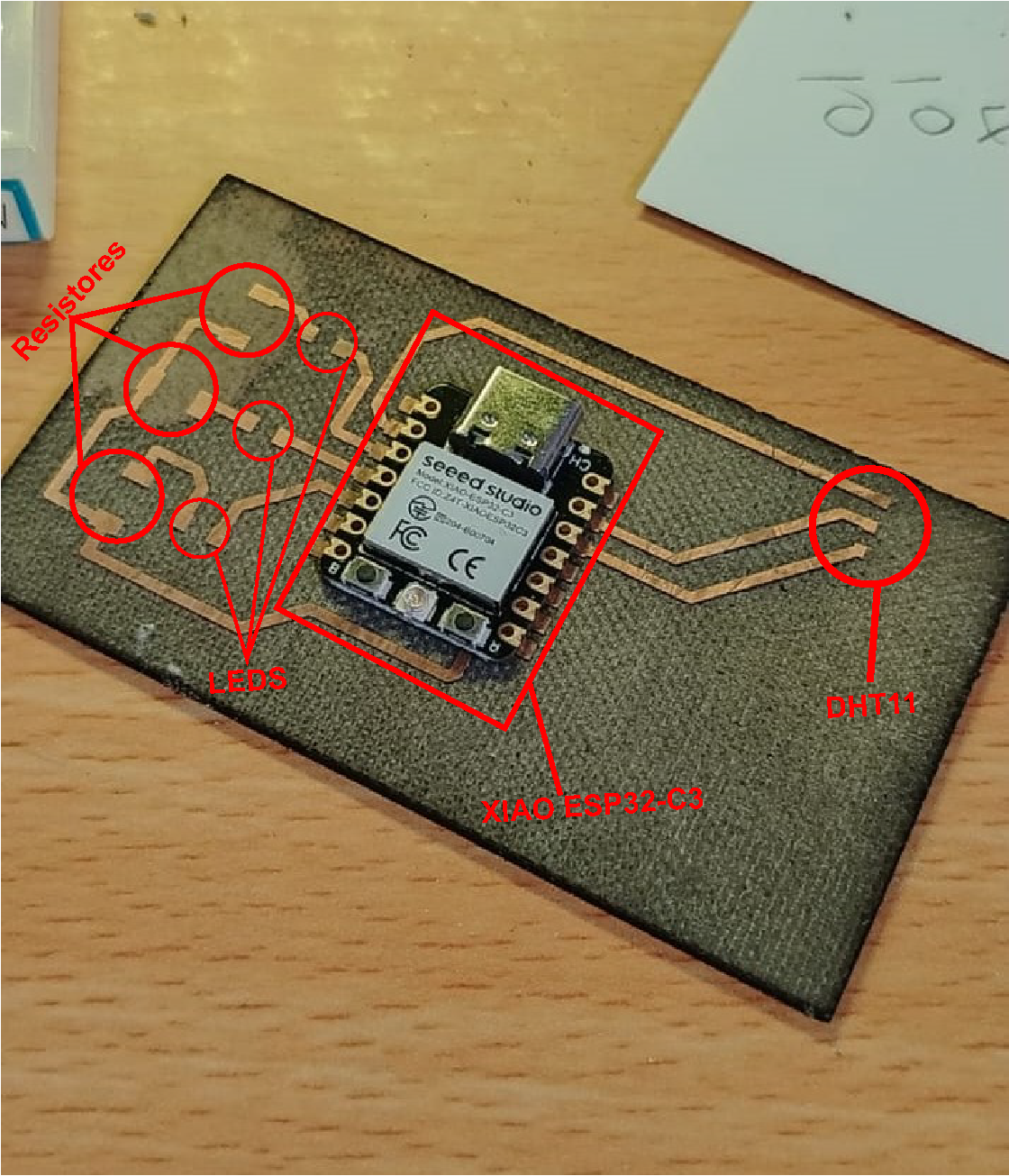
Below is the first PCB with the XIAO ESP32C3 already soldered. It was at this point, when I tried to solder the LEDs and resistors, that I realized they did not fit the component footprints.
After that, I returned to the design and modified the pad sizes for the resistors and LEDs so that they could make proper contact during soldering.
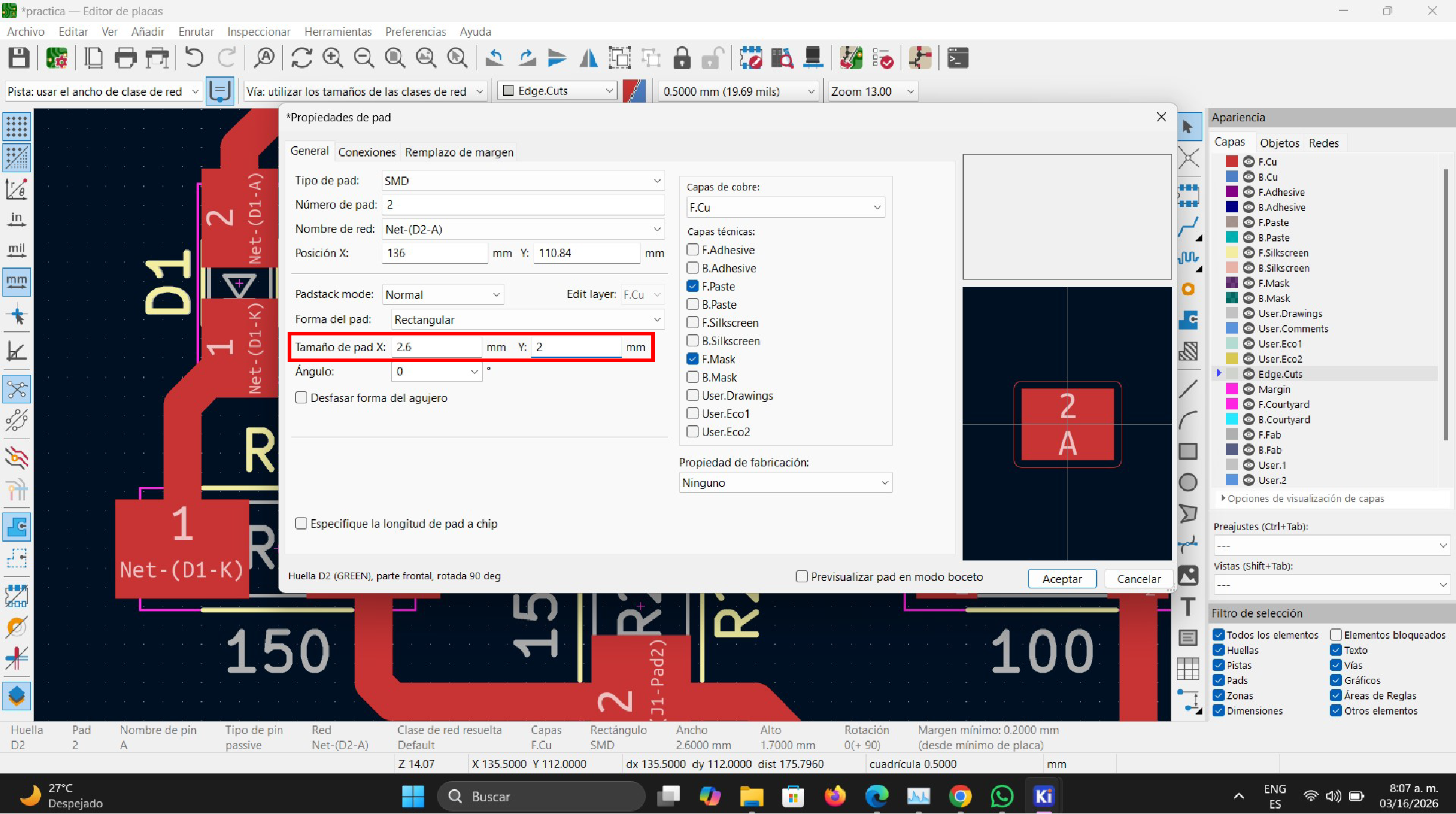
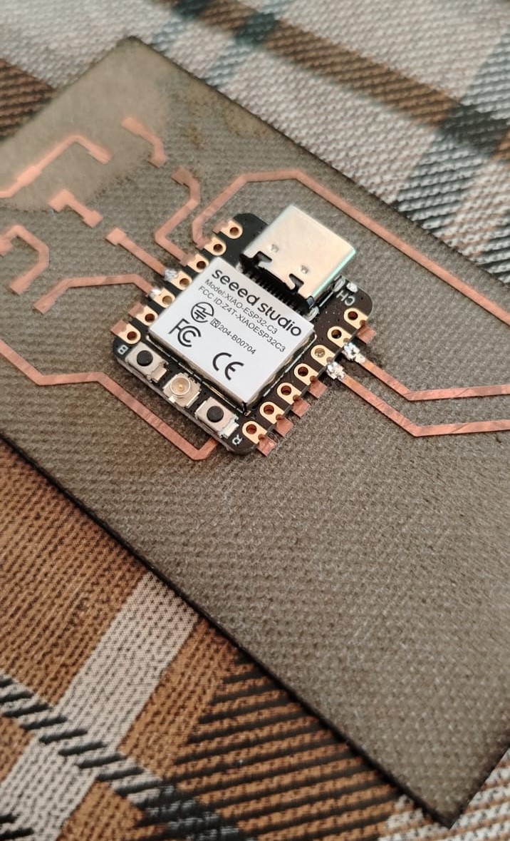
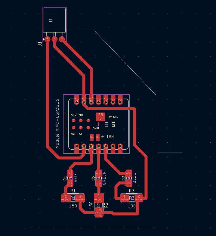
Once the pads were modified, I exported the design again and sent it to the xTool machine for engraving. In addition to modifying the pads, I also made some small design improvements such as changing the PCB shape and slightly reducing its size. The new PCB design now looks like this.
Next, the engraving process started.
Once the engraving process was completed, I proceeded with the PCB outline cutting process. For this step, I removed all the traces and left only the board outline. This was done without moving the PCB position either in the software or on the xTool machine bed.
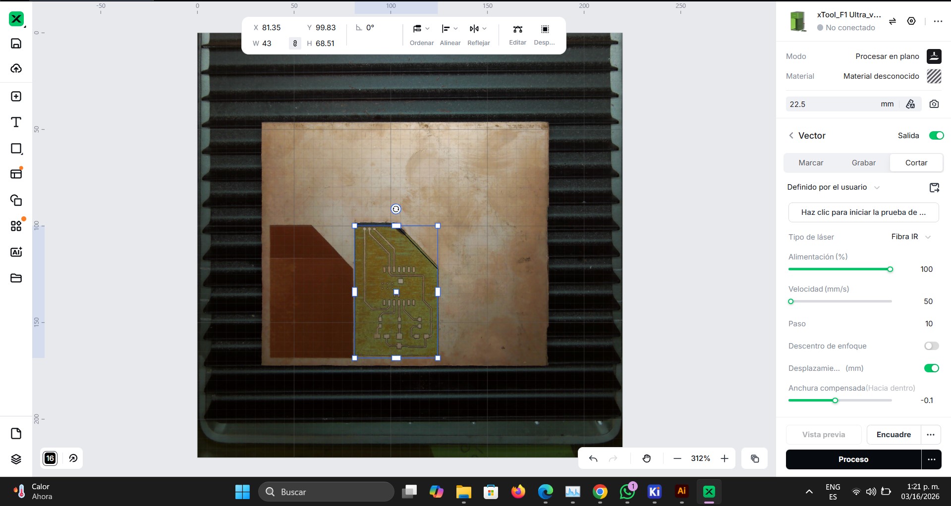
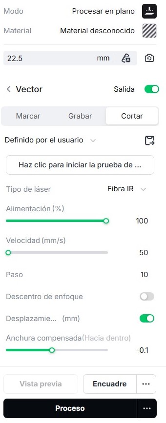
Then I configured the following cutting parameters as shown in the image below.
I used 100% laser power with a speed of 50 mm/s and performed 10 passes. Without moving the PCB from its position, I repeated the process with another 10 passes. This process was repeated four times until the board was completely cut.
Initially, when cutting the first board, I used a speed of 5 mm/s at 100% power. I do not recommend these values because they can generate flames during the cutting process, which is unsafe. For this reason, I finally used 100% power with a speed of 50 mm/s and multiple passes.
Once the board was fully cut, I removed it from the machine.
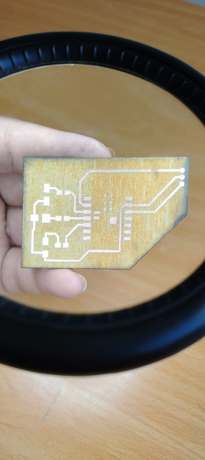
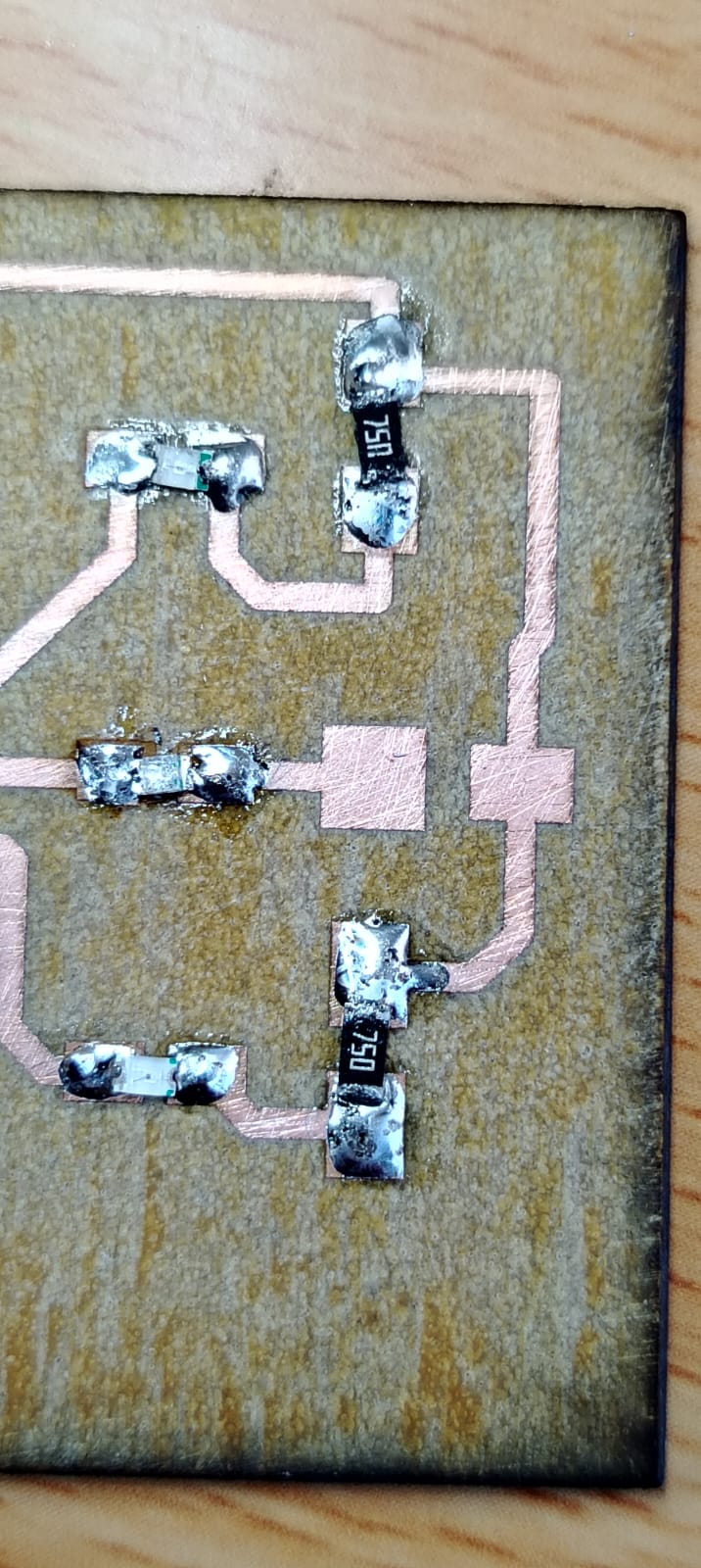
This is the final result of the newly fabricated PCB.
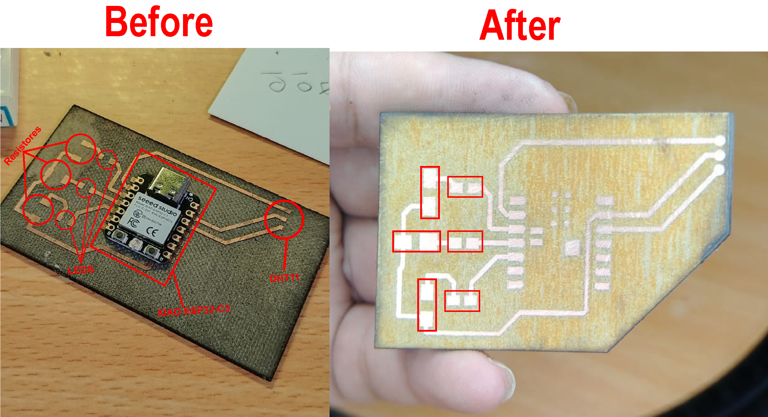
Below is a comparison showing the before and after results. The first PCB had very small pads, while the second design has larger pads, making it easier to solder the small components.
Now the board is ready for soldering. I started by soldering one LED. Before soldering, I checked its polarity using a multimeter to ensure it was placed in the correct orientation.
To solder the LED, I first applied solder to the pad area. Then I held the LED with fine tweezers, since these components are very small, and placed it in the correct position. Finally, I used the soldering iron tip to melt the solder that was previously applied so the LED could attach properly and make contact with the copper trace. This process was repeated for all LEDs.
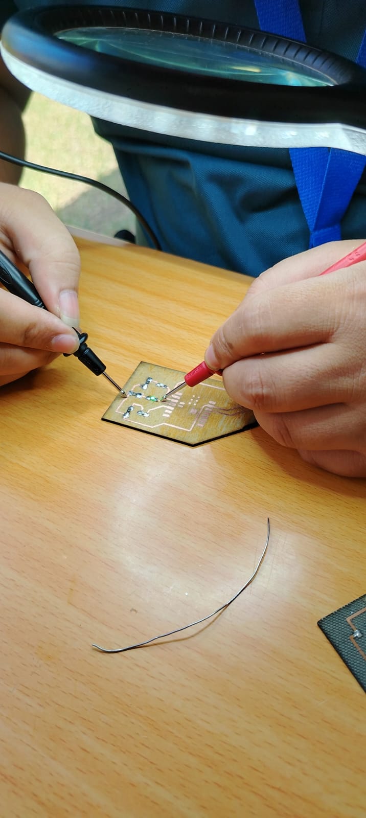
After that, I verified the electrical connections using a multimeter.
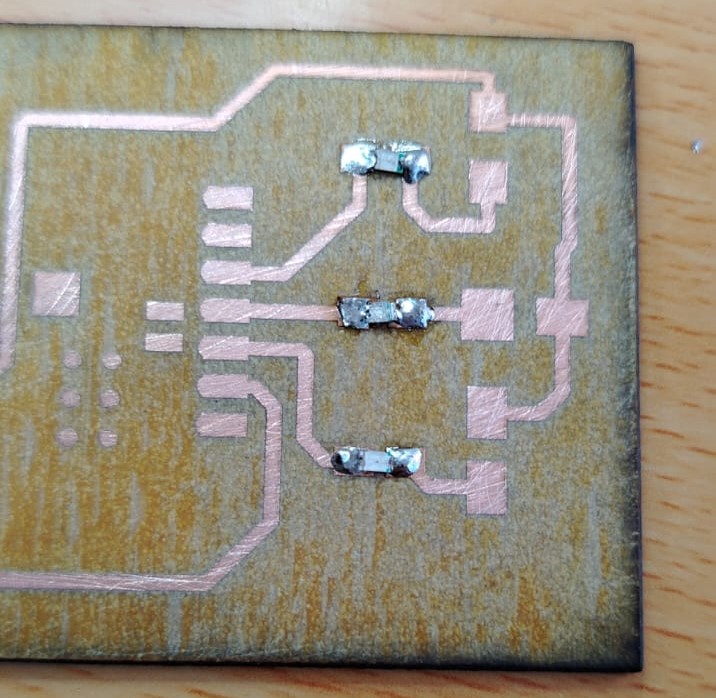
Next, I soldered the resistors. I used three surface-mount resistors: two 75 ohm resistors and one 220 ohm resistor. As mentioned before, these components were recovered from old electronic devices.
I used the same soldering method used for the LEDs. It is important to mention that resistors do not have polarity, so their orientation does not matter.
After soldering the resistors, I verified the electrical connections again using a multimeter. Everything was working correctly.
Finally, I soldered the XIAO ESP32C3 module onto the PCB and added header pins to connect the DHT11 sensor using female-to-female jumper wires.
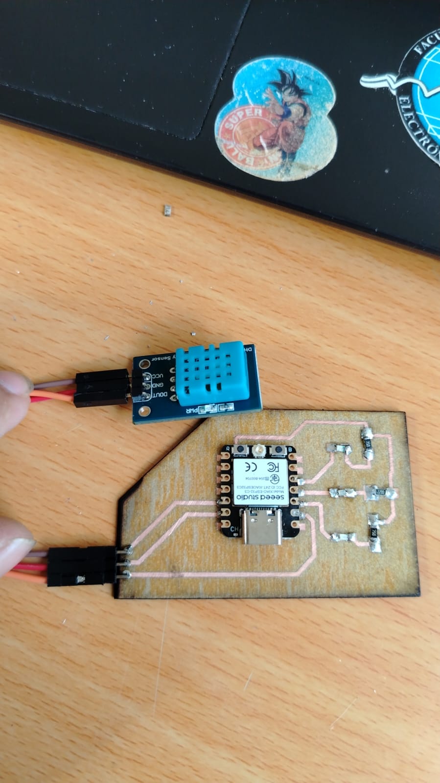
Once the board was fully assembled, I performed a functionality test by writing a program in Arduino IDE. The program changes the LED color depending on the temperature measured by the DHT11 sensor. For example, if the temperature is higher than 28 °C the red LED turns on; if the temperature is between 20 °C and 28 °C the green LED turns on; and if the temperature is below 20 °C the blue LED turns on. The code is shown below.
                            #include

                            #define DHTPIN D1        // Pin donde conectas el DHT11
                            #define DHTTYPE DHT11

                            #define LED_AZUL D4
                            #define LED_VERDE D3
                            #define LED_ROJO D2

                            DHT dht(DHTPIN, DHTTYPE);

                            void setup() {

                            Serial.begin(115200);

                            pinMode(LED_AZUL, OUTPUT);
                            pinMode(LED_VERDE, OUTPUT);
                            pinMode(LED_ROJO, OUTPUT);

                            dht.begin();
                            }

                            void loop() {

                            float temperatura = dht.readTemperature();

                            if (isnan(temperatura)) {
                                Serial.println("Error leyendo el sensor DHT11");
                                return;
                            }

                            Serial.print("Temperatura: ");
                            Serial.print(temperatura);
                            Serial.println(" °C");

                            // Apagar todos los LEDs primero
                            digitalWrite(LED_AZUL, LOW);
                            digitalWrite(LED_VERDE, LOW);
                            digitalWrite(LED_ROJO, LOW);

                            // Condiciones de temperatura
                            if (temperatura < 20) {
                                digitalWrite(LED_AZUL, HIGH);
                            }
                            else if (temperatura >= 20 && temperatura <= 28) {
                                digitalWrite(LED_VERDE, HIGH);
                            }
                            else {
                                digitalWrite(LED_ROJO, HIGH);
                            }

                            delay(2000);
                            }
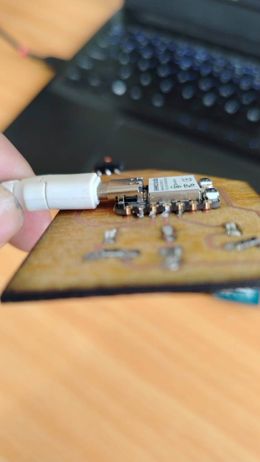
To upload this code to the board, we connect the PCB to the computer using a USB-C cable.
In the Arduino IDE we select the board we are using, which in this case is the XIAO ESP32C3, and then select the corresponding port. In my case the port is COM7. After that, we upload the code to the XIAO ESP32C3 module using the USB-C cable.
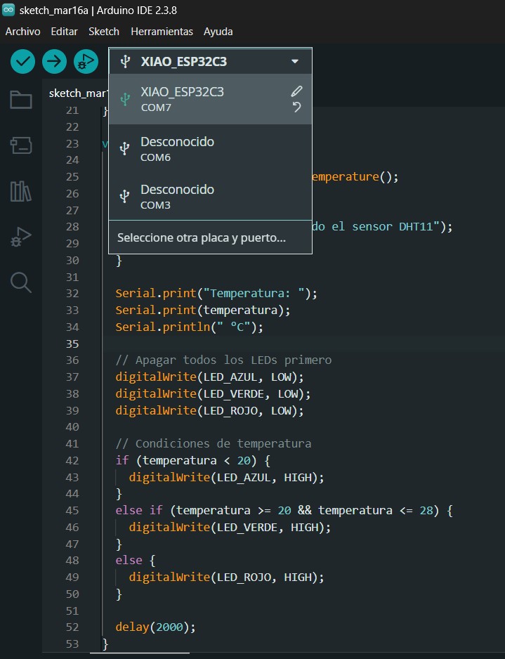
Once the board and port are configured, we upload the code to the microcontroller.
When the temperature measured by the DHT11 sensor is between 20 °C and 28 °C, the green LED turns on.
When the temperature measured by the DHT11 sensor is higher than 28 °C, the red LED turns on.
When the temperature measured by the DHT11 sensor is lower than 20 °C, the blue LED turns on.
What I learned
During this week I learned how to manufacture my own PCB board. It is not the most beautiful one, but I made it myself 🙈. I also learned how to modify the design and realized that pads are very important, so their size must be defined beforehand to avoid the problem I had.
I learned how to engrave and cut PCB boards using the Xtool machine.
I also had the experience of soldering very small SMD components. In addition, I learned how to look for components from other damaged devices in order to reuse them.
Honestly, both week 6 and this week were very enriching. I learned a lot about PCB manufacturing, from the design stage all the way to the fabrication process.
Dowload File
Mission accomplished! 😊