Group assignment
Objective
-
Use the test equipment in your lab to observe the operation of a microcontroller circuit board (as a minimum, you should demonstrate the use of a logic analyzer)
-
Document your work on the group work page and reflect on your individual page what you learned
Here I share the link to my group assignment.
Explaind what you learned
During this assignment, I gained valuable knowledge about how fundamental electronic measurement tools work and understood why they are essential in any circuit design process. By working with devices such as the multimeter, oscilloscope, and logic analyzer, I learned not only how to measure electrical properties like voltage, current, and resistance, but also how to interpret these measurements to diagnose and understand circuit behavior.
This experience taught me the importance of performing careful measurements and verifications in electronics: from ensuring that components operate within expected ranges to confirming that digital signals behave correctly. I also realized that using these tools responsibly and methodically helps prevent errors and leads to more reliable and accurate design decisions. This skill is fundamental in digital fabrication and electronic prototyping, and it will continue to benefit me in future projects.
Indivual assignment
Use an EDA tool to design a development board that uses parts from the inventory to interact and communicate with an embedded microcontroller
Before using KiCad, I ran a simulation on Wokwi of the circuit I will design to read the ambient humidity and temperature.
Simulation
The PCB design and development process will be carried out using KiCad, with the XIAO ESP32-C3 serving as the primary microcontroller for the system.
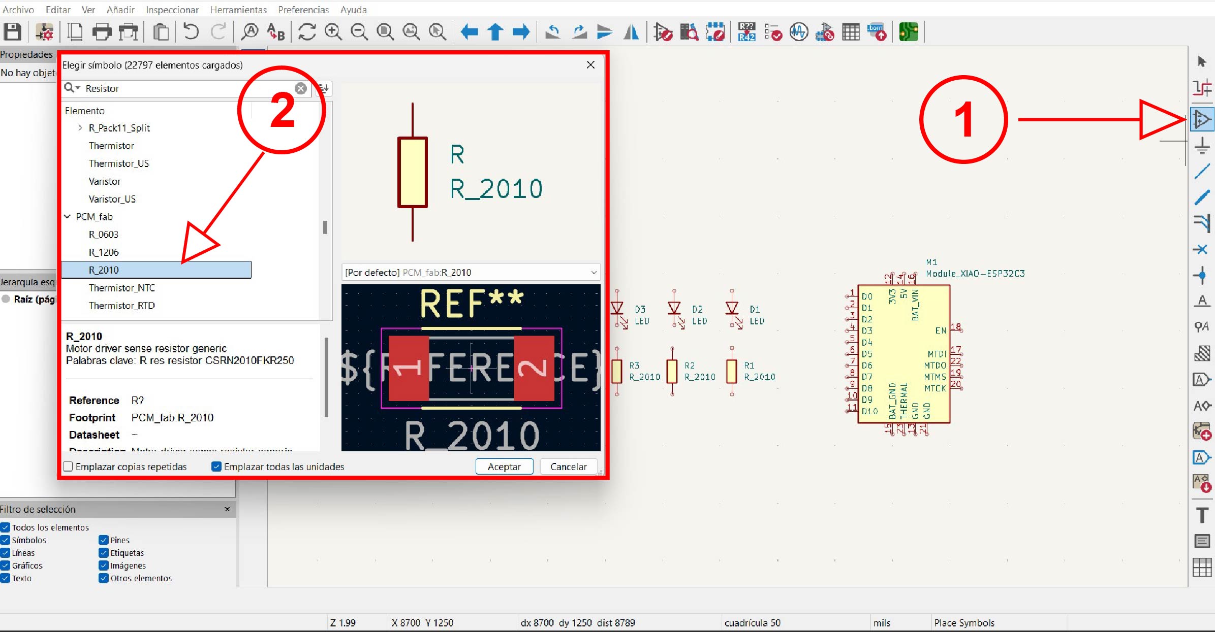
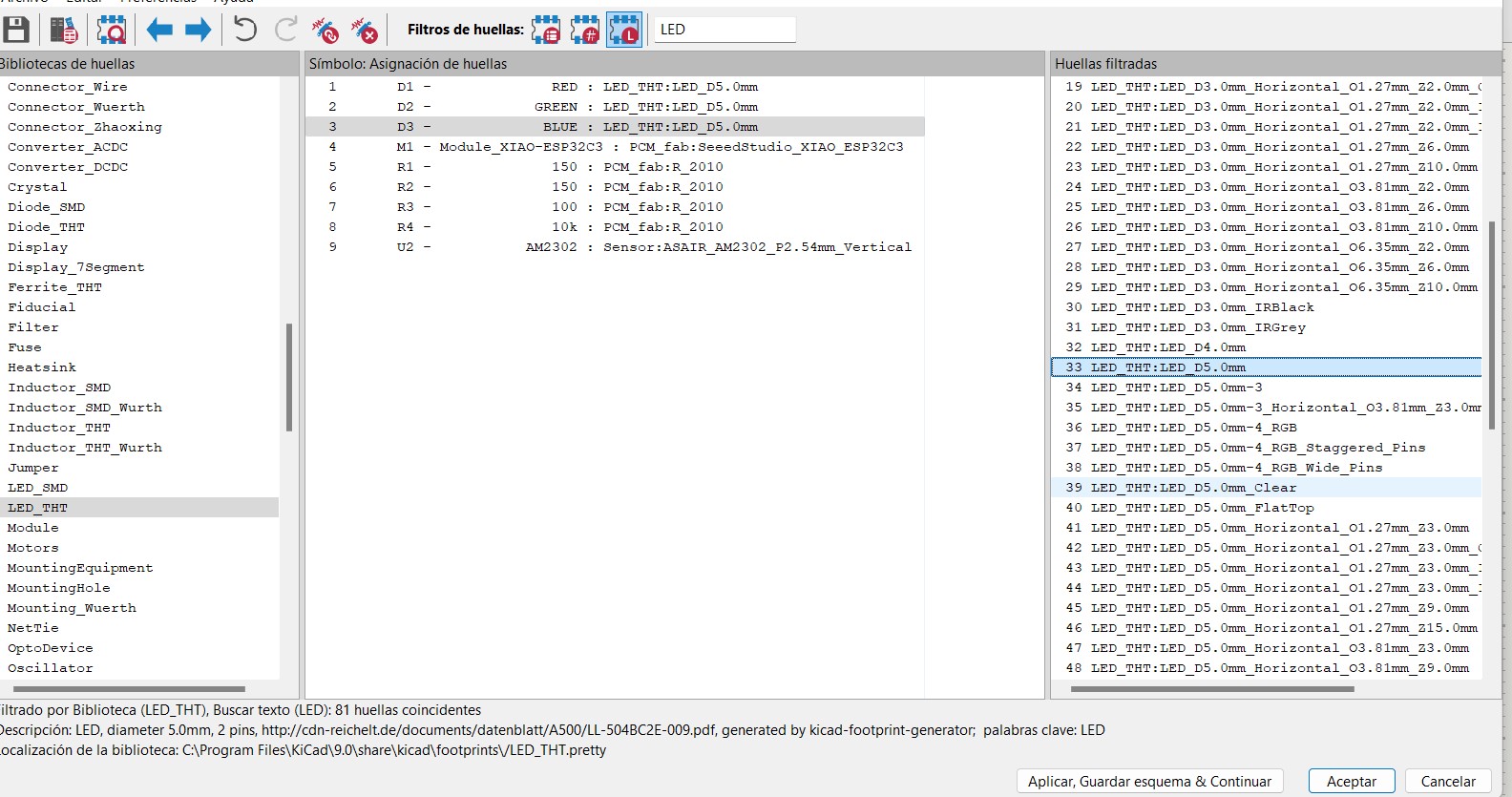
The first step in the design process is to add the required components to the schematic in KiCad.
Components
The components I will use for this project are:
- DHT22 sensor, also known as AM2302
- XIAO ESP32-C3
- Resistors
- LEDs
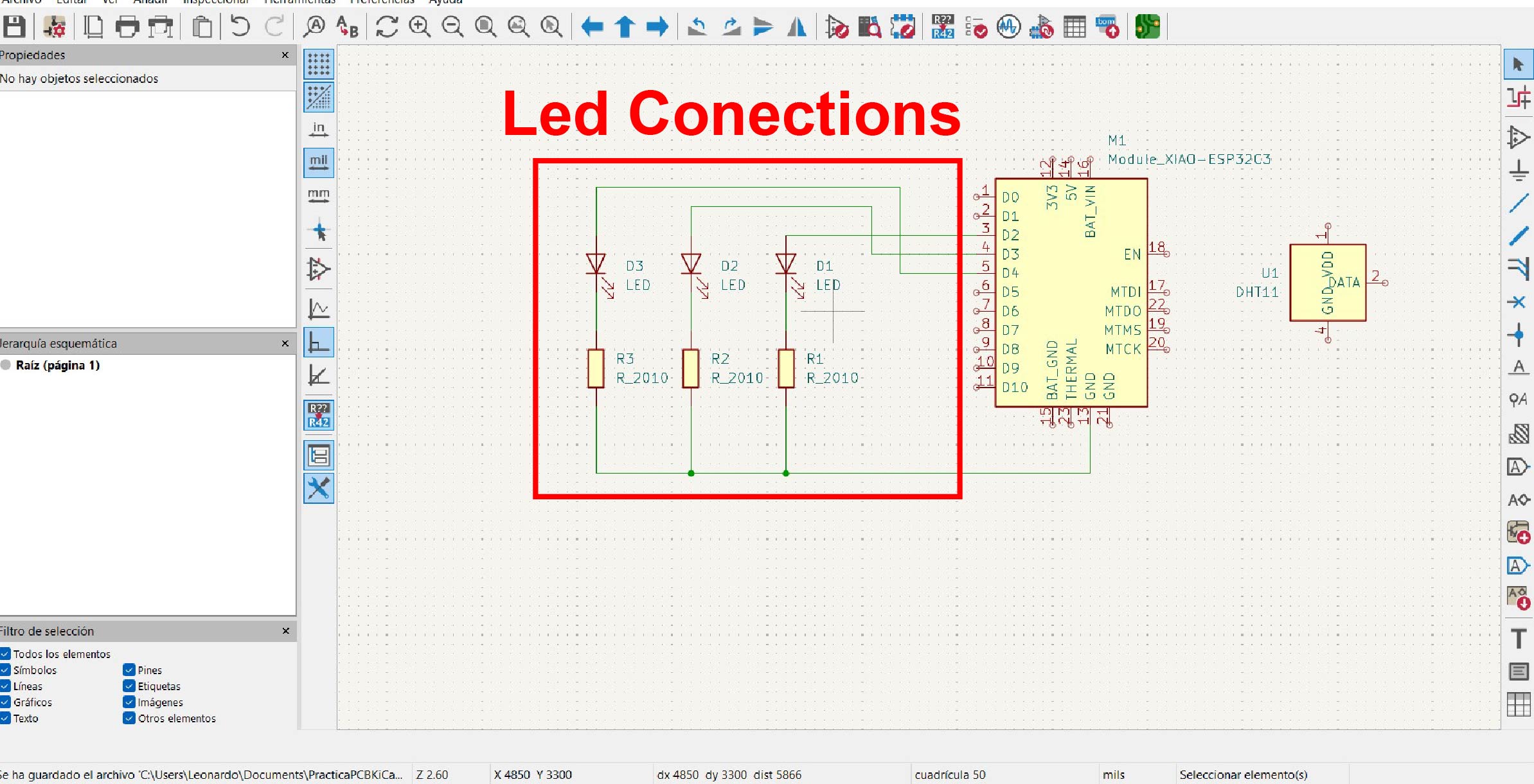
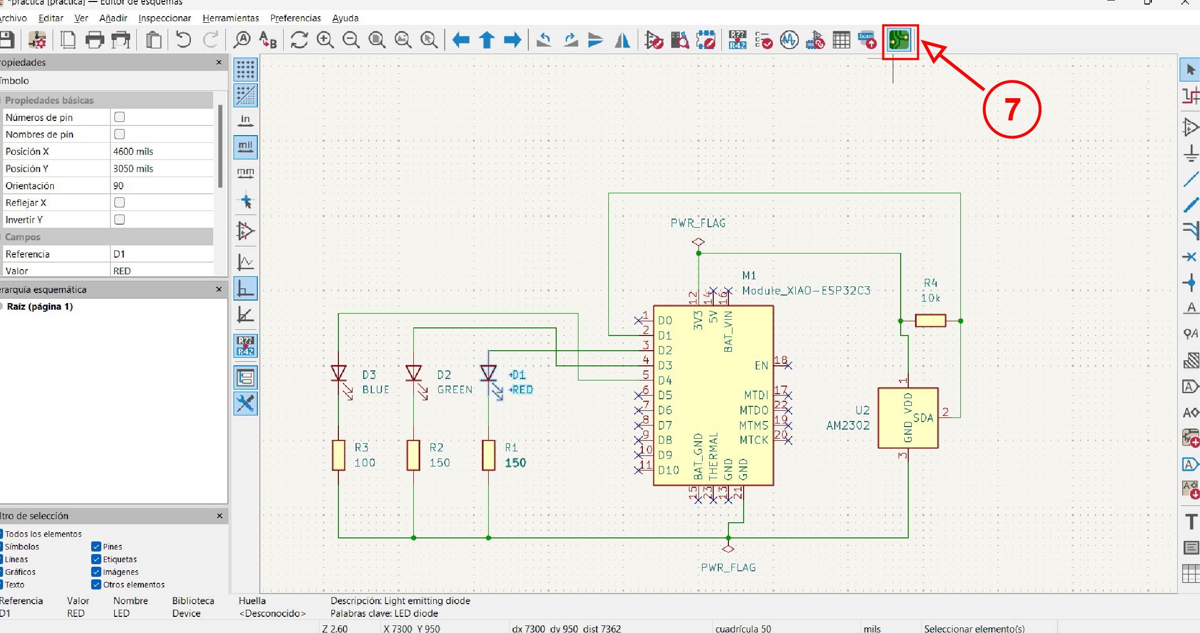
In the second stage, the LEDs were connected to the general-purpose input/output (GPIO) pins of the XIAO ESP32-C3 within the schematic design.
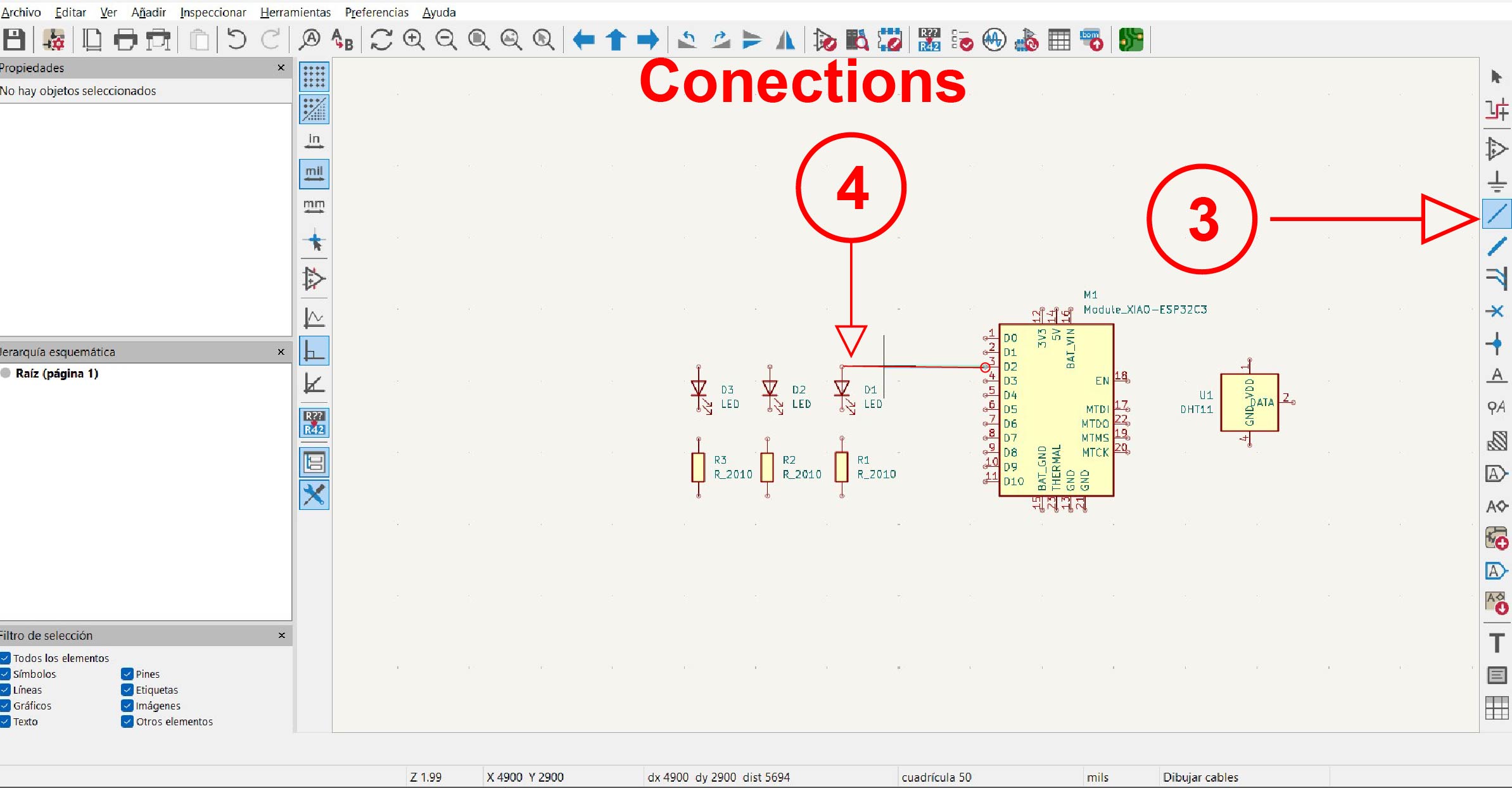
Subsequently, the DHT22 temperature and humidity sensor was connected to the XIAO ESP32-C3.
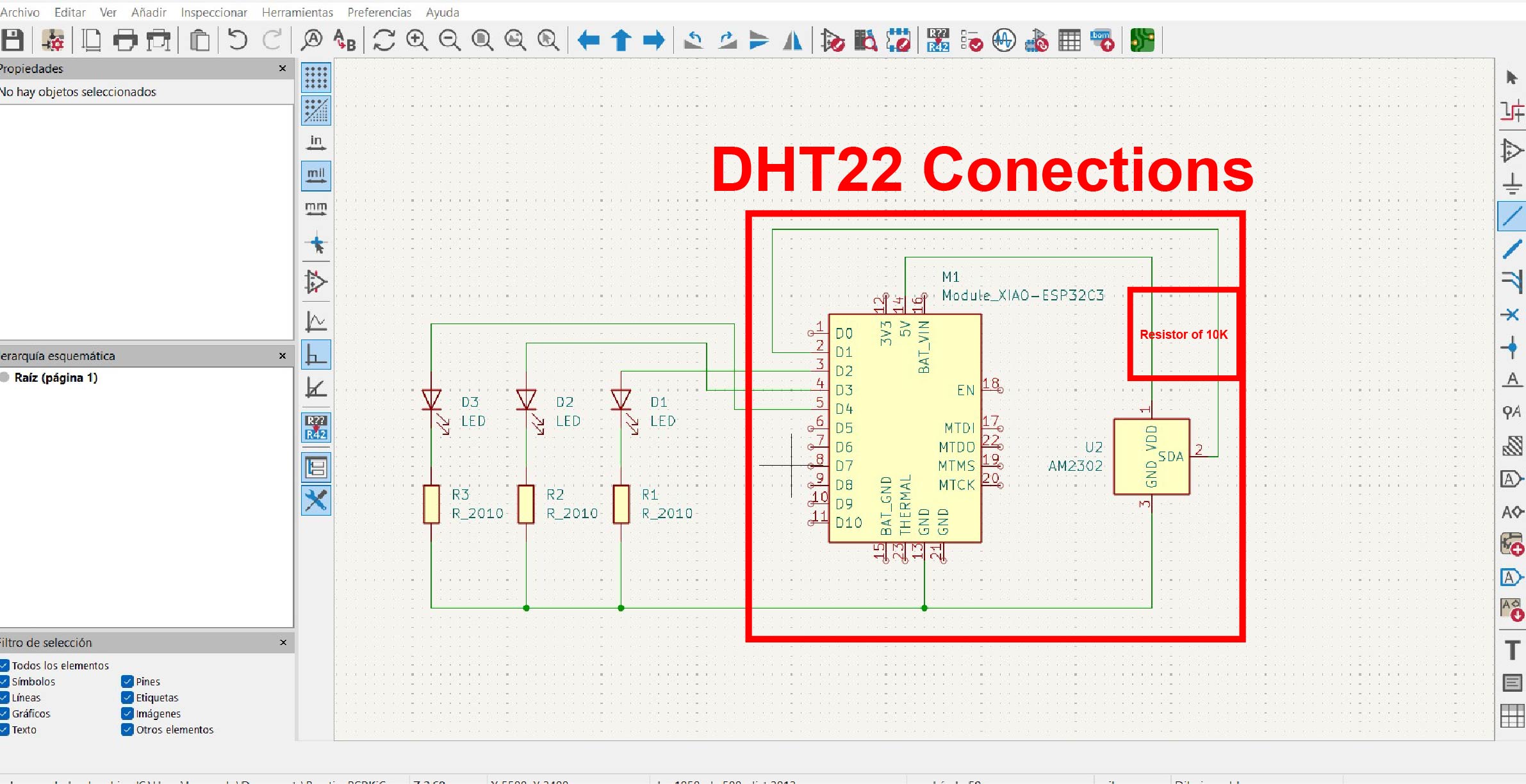
Based on the DHT22 datasheet, it is advised to include a 5 kΩ – 10 kΩ pull-up resistor between the VCC and DATA line to enhance data communication stability, as recommended in the official documentation. (Refer to datasheet) The final schematic is shown in the image below.
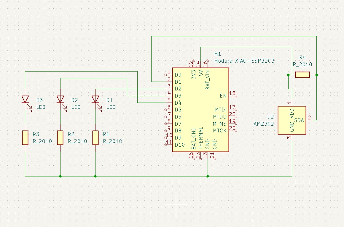
DHT22 Sensor Connections
| Component | Sensor Pin | Connected To | Description |
|---|---|---|---|
| DHT22 | VCC | 5V | 5V Power Supply |
| DHT22 | DATA | D1 (GPIO) | Digital Data Signal |
| DHT22 | GND | GND | Common Ground |
| Resistor | 10kΩ | Between VCC and DATA | Pull-up resistor required for communication |
LED Connections
| Component | XIAO Pin | Connected To | Description |
|---|---|---|---|
| Red LED | D2 | 220Ω Resistor → GND | High temperature indicator |
| Green LED | D3 | 220Ω Resistor → GND | Normal temperature indicator |
| Blue LED | D4 | 220Ω Resistor → GND | Low temperature indicator |
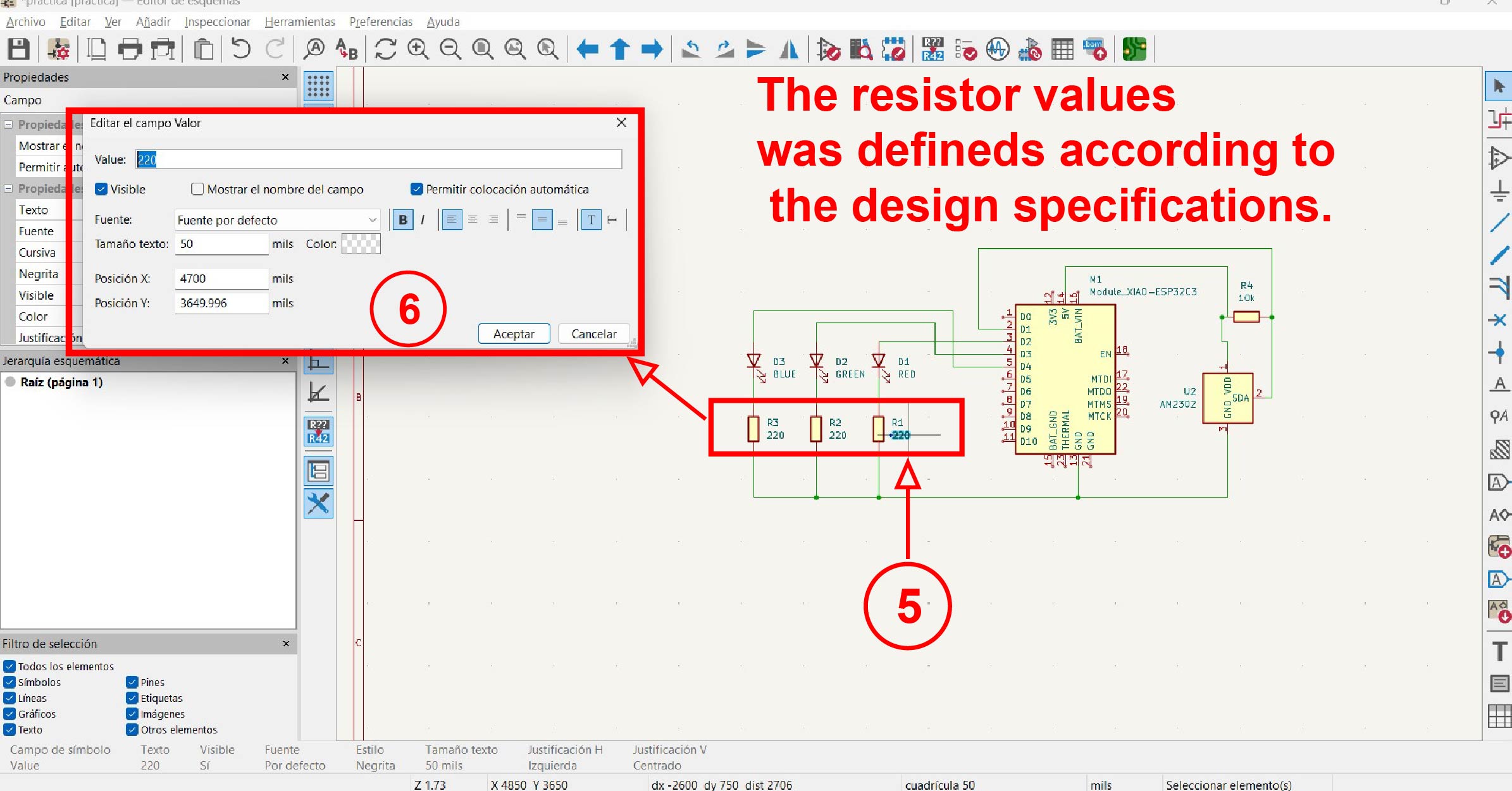
The resistor value was calculated using Ohm’s Law.
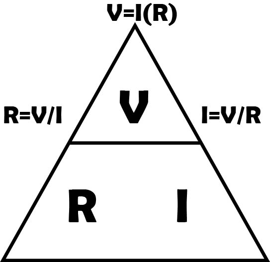
To calculate the resistor value, I used the formula R = V / I , which states that resistance equals voltage divided by current.
LED Resistor Calculation
To calculate the resistor value for the LED connected to the XIAO ESP32-C3 (3.3V output), Ohm’s Law was applied using the following formula:
Where:
- R = Resistance (Ohms, Ω)
- Vsource = Supply voltage (3.3V)
- VLED = Forward voltage of the LED
- ILED = Desired LED current (Amperes)
Calculation (Red LED)
Assuming:
- Supply Voltage = 3.3V
- LED Forward Voltage = 1.8V
- Desired Current = 10mA (0.01A)
Calculation (Led Green)
Assuming:
- Supply Voltage = 3.3V
- LED Forward Voltage = 1.8V
- Desired Current = 10mA (0.01A)
Calculation (Led Blue)
Assuming:
- Supply Voltage = 3.3V
- LED Forward Voltage = 2.8V
- Desired Current = 10mA (0.01A)
The closest commercial resistor values are 150Ω or 220Ω. For safety and GPIO protection, a 220Ω resistor is recommended.
Electrical control ruls
Initially, this was the schematic I was working with.
However, when running the ERC (Electrical Rules Check), errors appeared as shown in the image below.
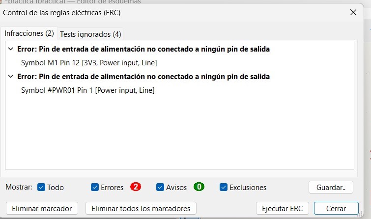
To fix one of the errors, I made some changes to the schematic: instead of connecting the DHT22 VDD to 5V, I connected it to the 3.3V pin of the XIAO ESP32-C3 and added a PWR_FLAG symbol.
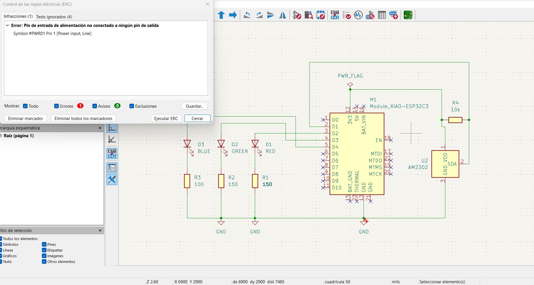
Now only one error is displayed, which indicates that I’m on the right track. To fix it, I added a PWR_FLAG symbol, and with this, the ERC (Electrical Rules Check) no longer shows any electrical errors.
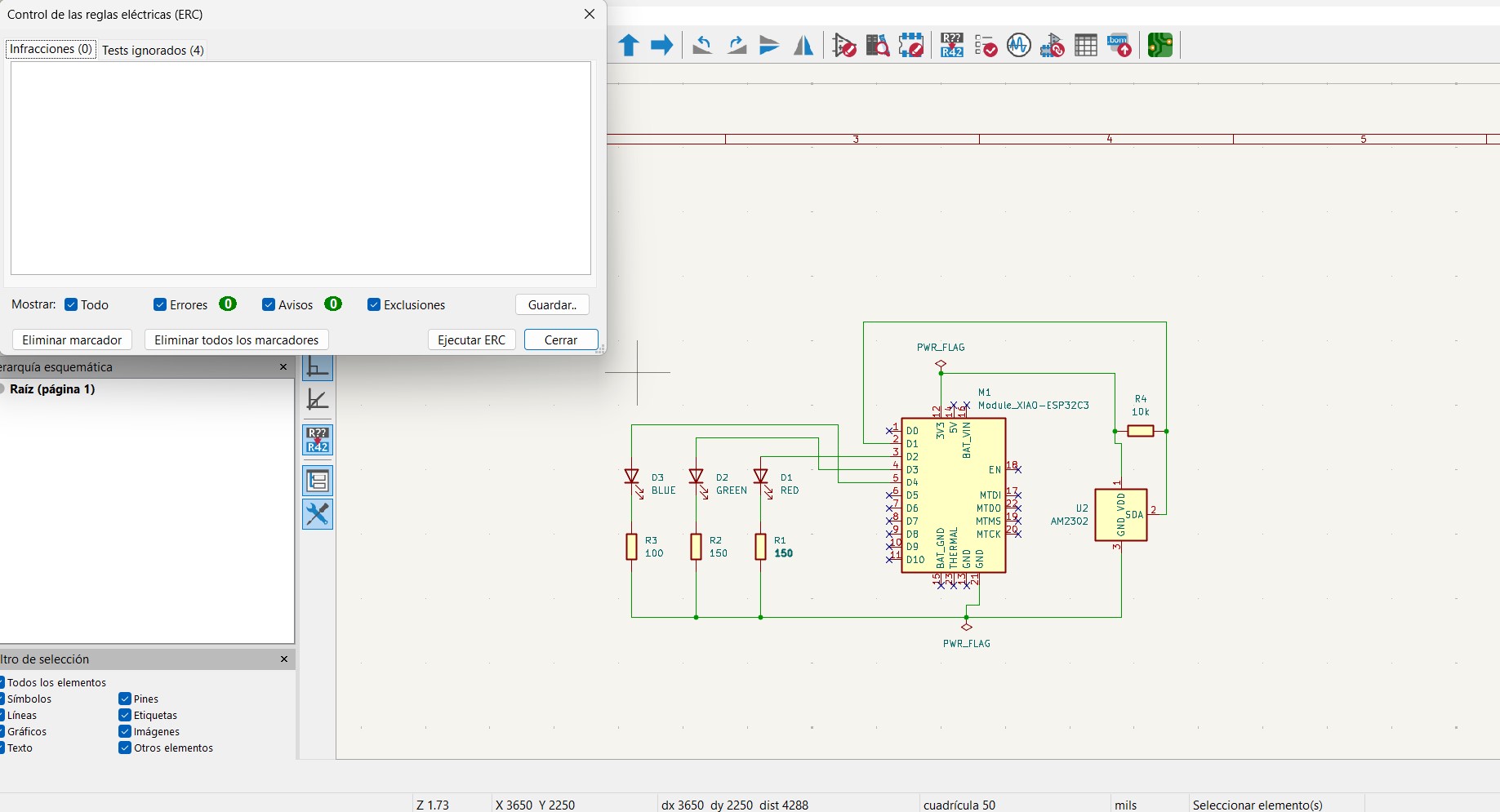
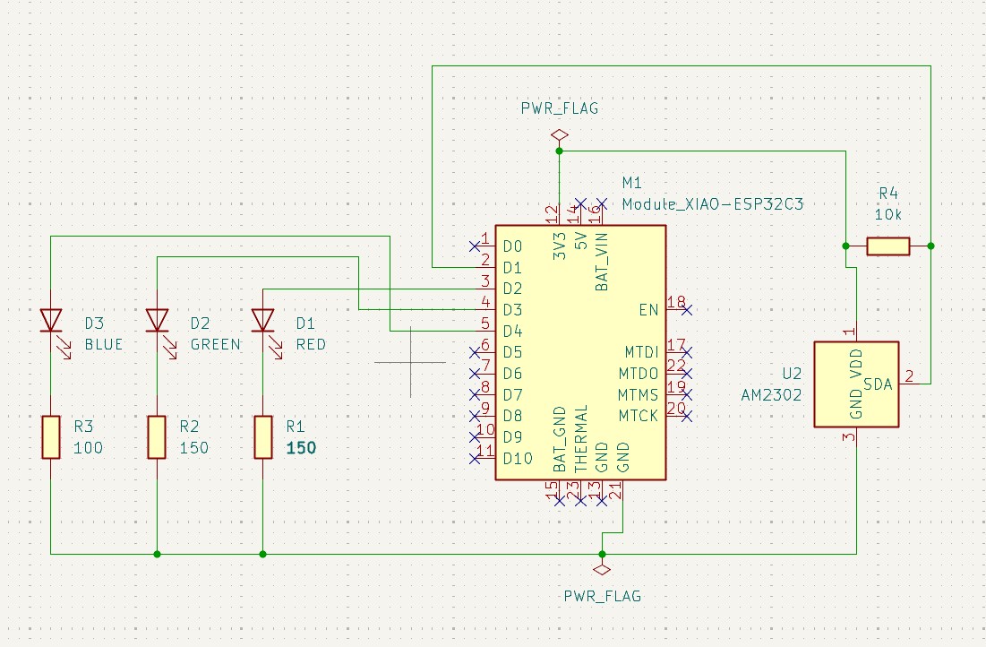
New schematic
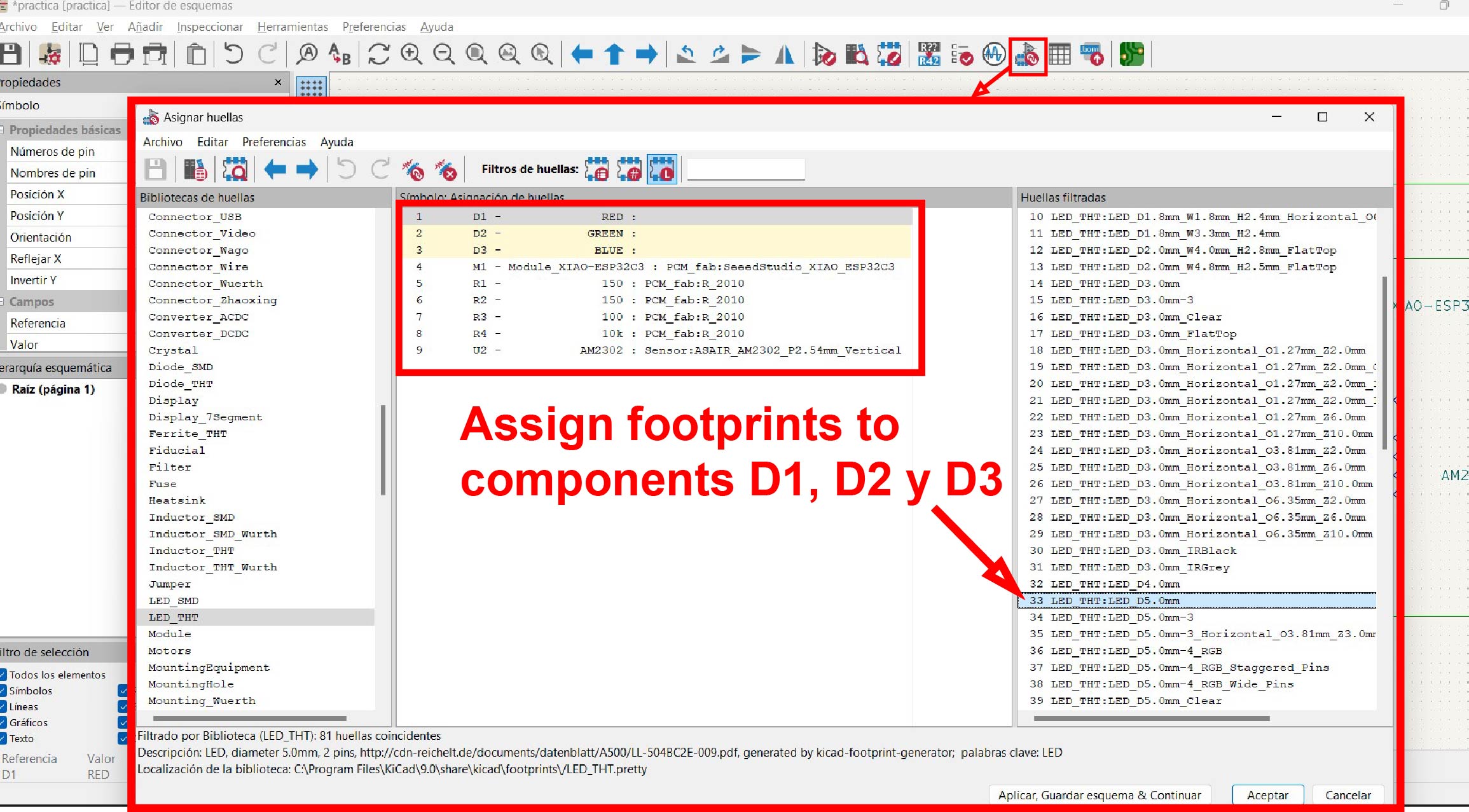
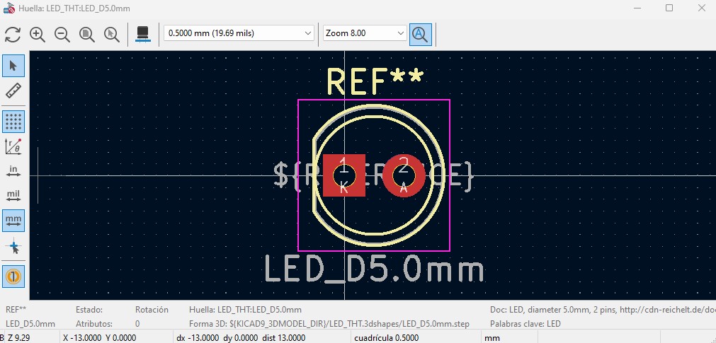
The next step in designing our PCB is to assign the appropriate footprints to each component. In this case, we assigned footprints to the LEDs, since they previously did not have any defined in the schematic.
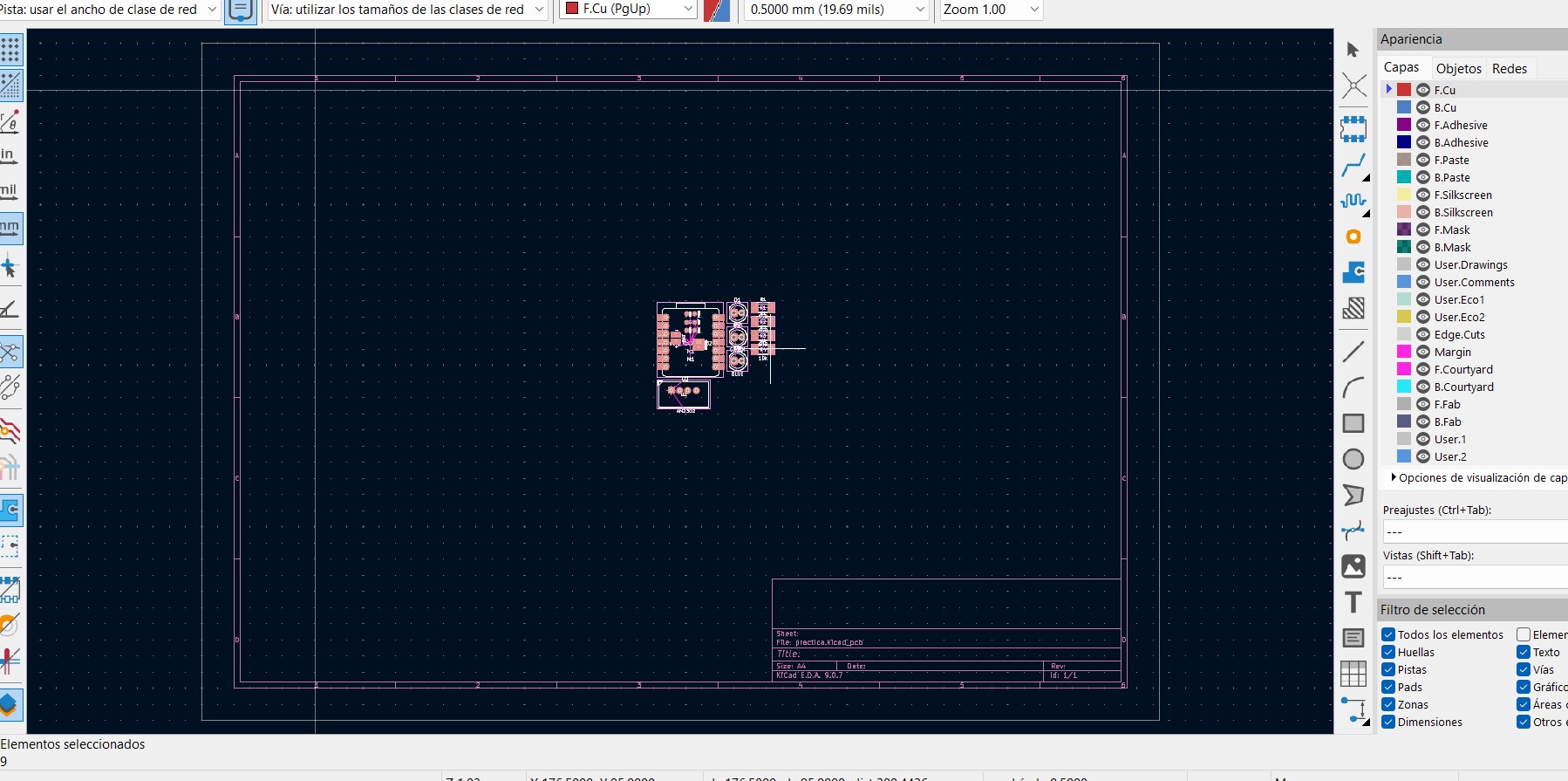
Once the footprints have been assigned to all components, the next step is to create the PCB layout, where we arrange and position the components on the board to begin the routing process.
We loaded our schematic into the PCB editor to begin the routing process, where we connect the traces according to the connections previously defined in the diagram.
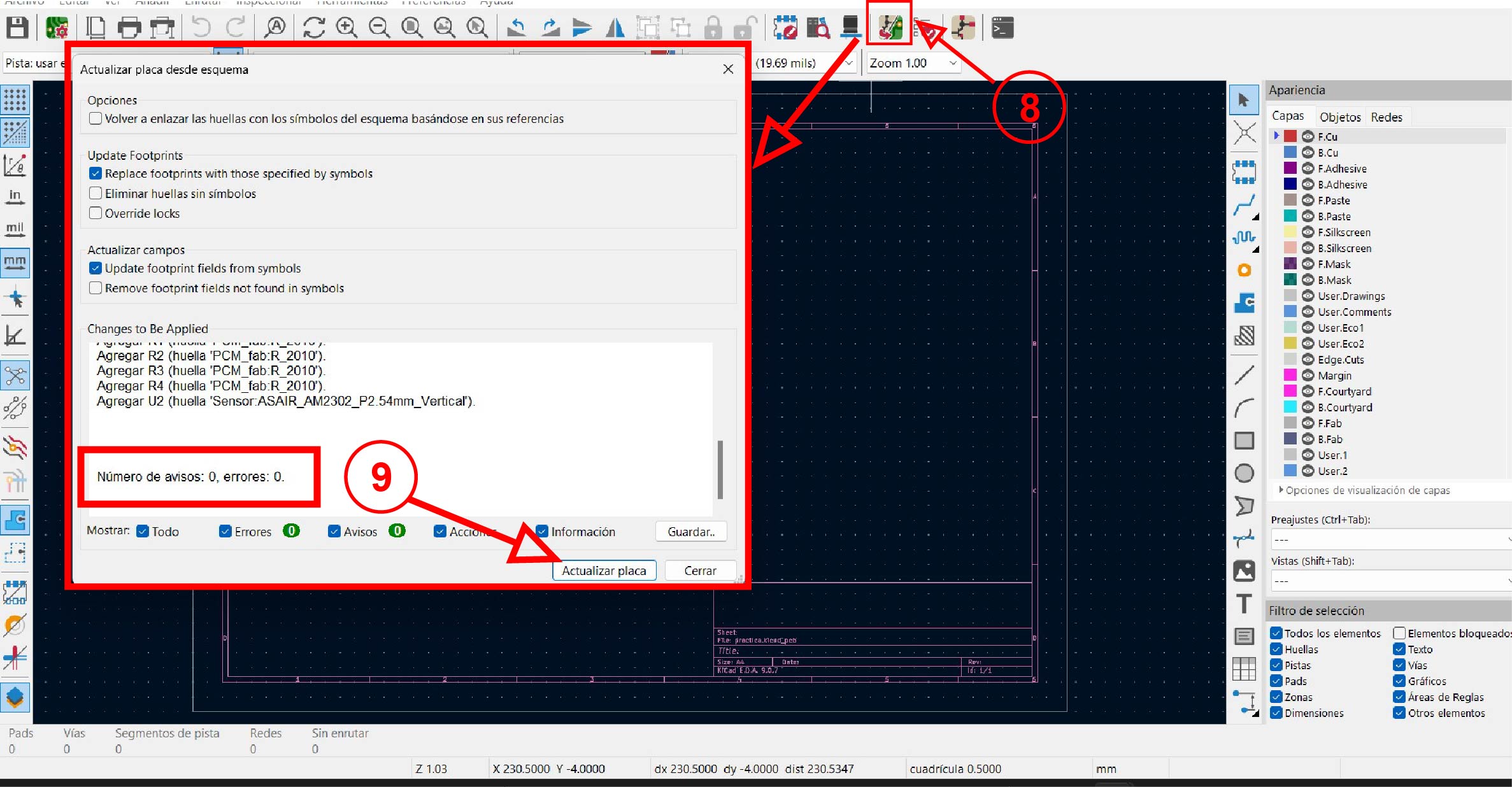
Once the board is loaded, we begin organizing our components, making sure that the connection lines are not tangled, which helps achieve a cleaner and more organized routing process.
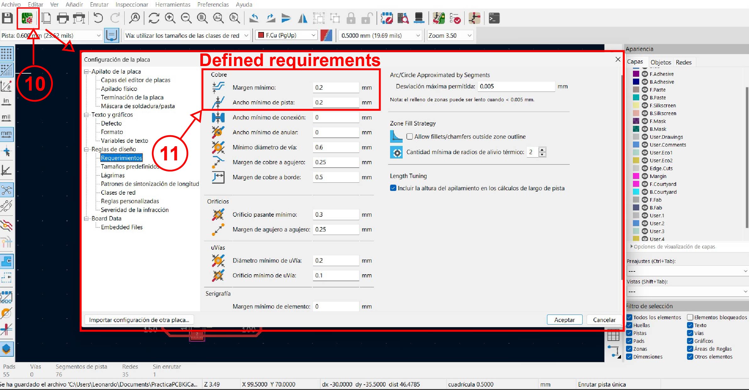
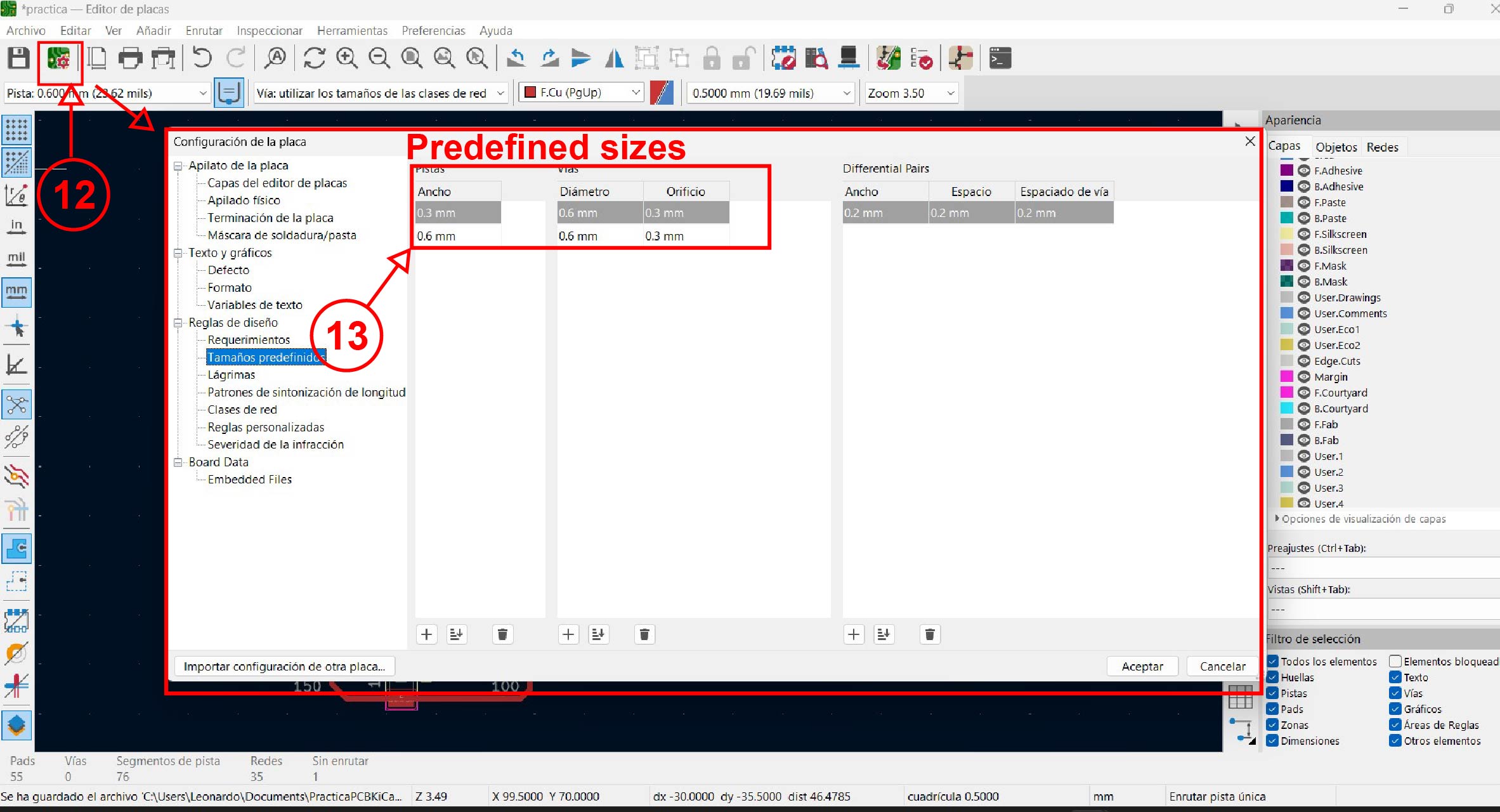
To begin the routing process, I defined the design rules. At this stage, I configured the track widths: signal traces were set to 0.3 mm, while the trace connecting the 3.3V pin of the XIAO ESP32-C3 to the VDD of the temperature and humidity sensor was set to 0.6 mm to ensure better current-carrying capacity and improved electrical robustness.
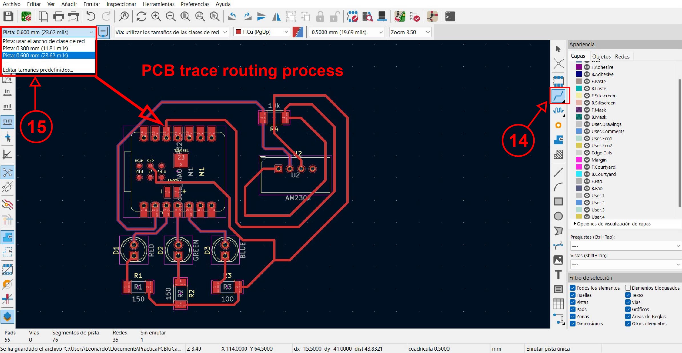
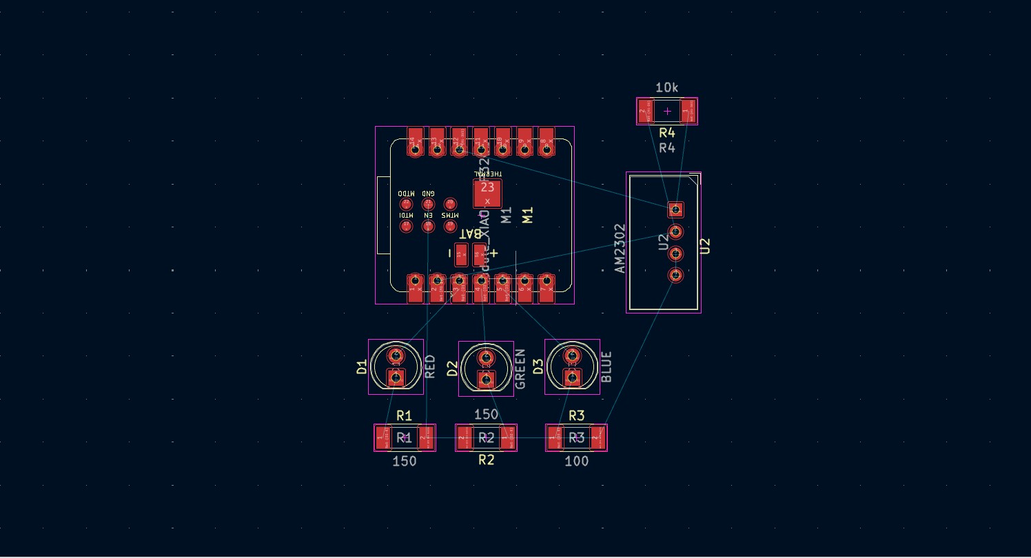
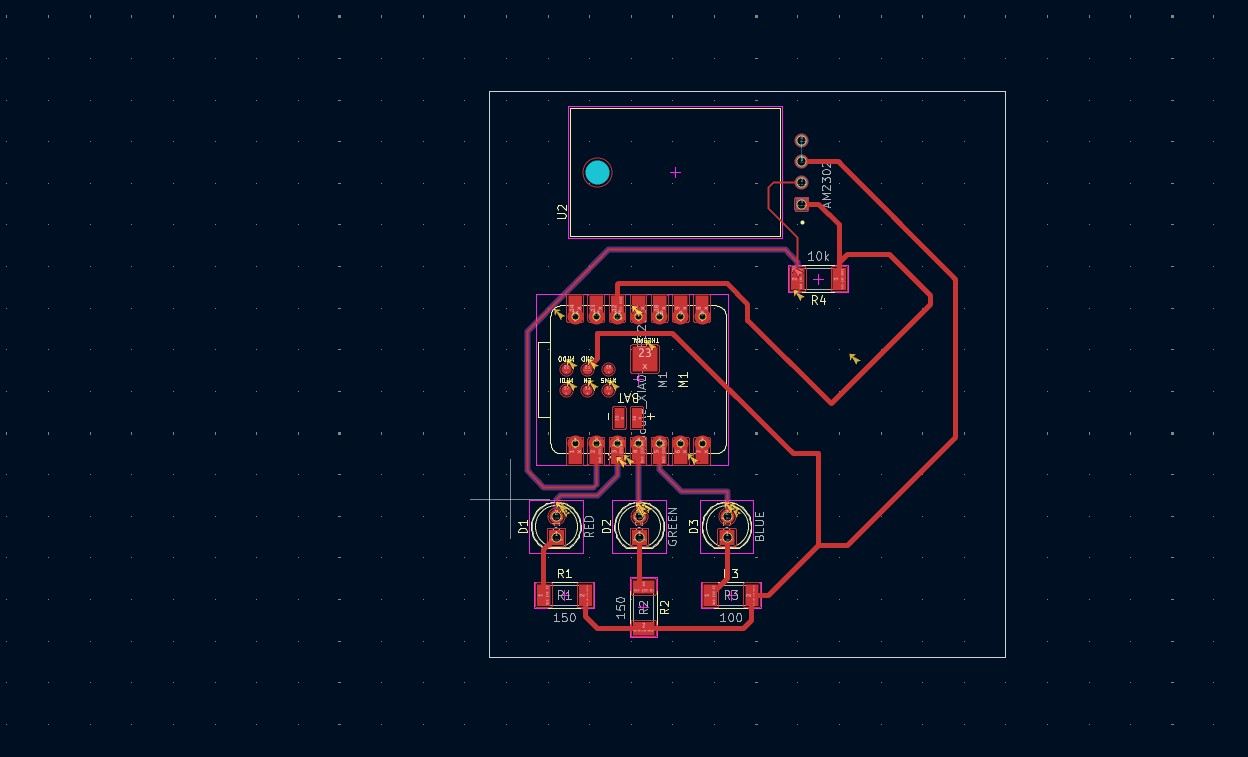
During the routing process, I rearranged the green LED resistor and the DHT22 sensor to optimize the component layout on the board. Once the routing was completed, I proceeded to define the board outline and delimit the PCB area.
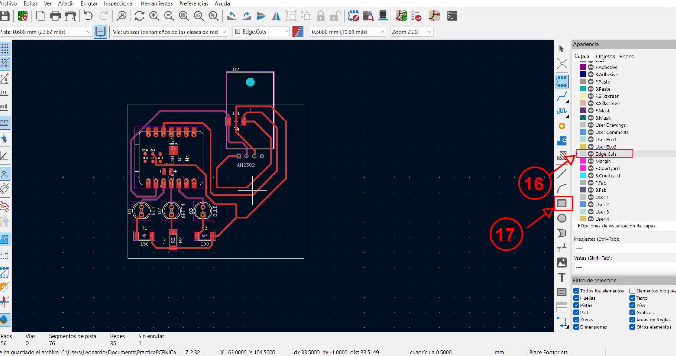
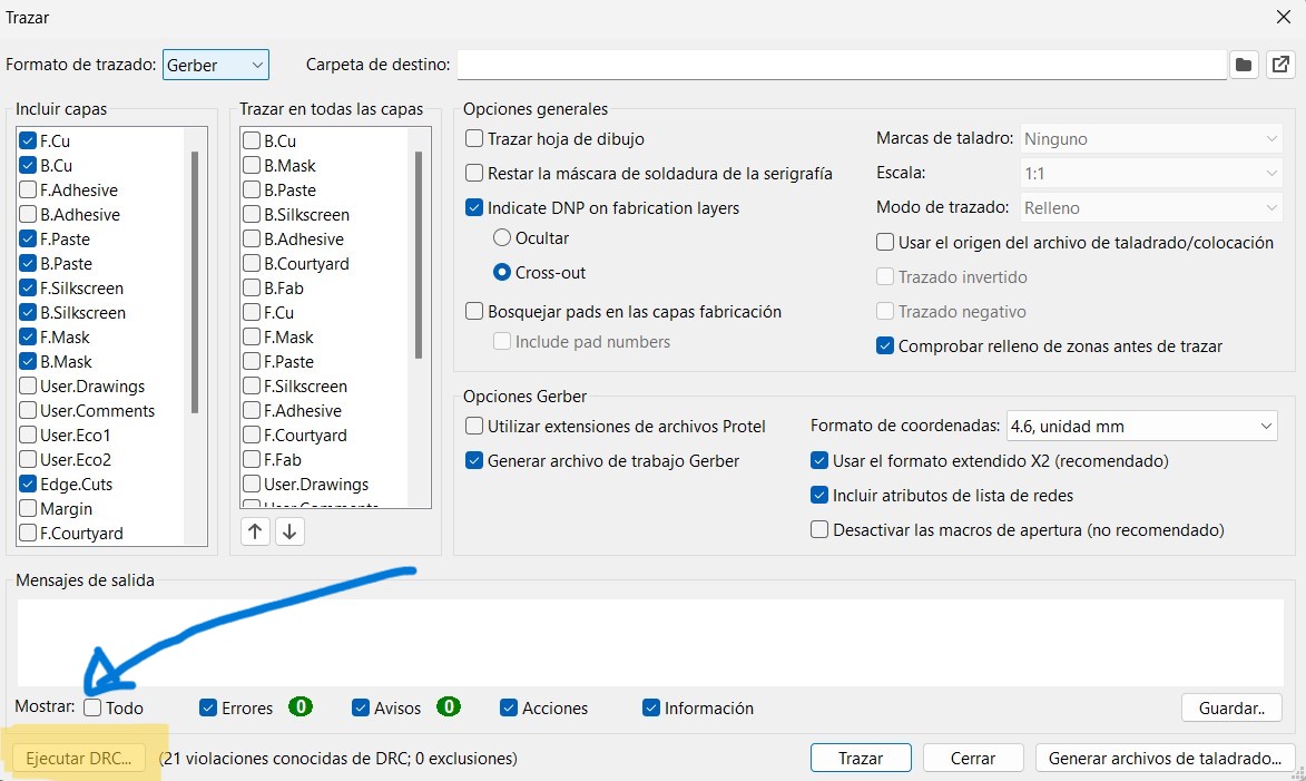
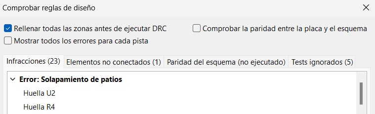
Once I reached this stage, I ran the DRC and a footprint overlap error appeared.
To fix this error, I rearranged the component layout, especially the DHT22, since its footprint was overlapping with the 10K resistor footprint. Once I reorganized the design, it looked as follows:
Once I made this change, the error disappeared.
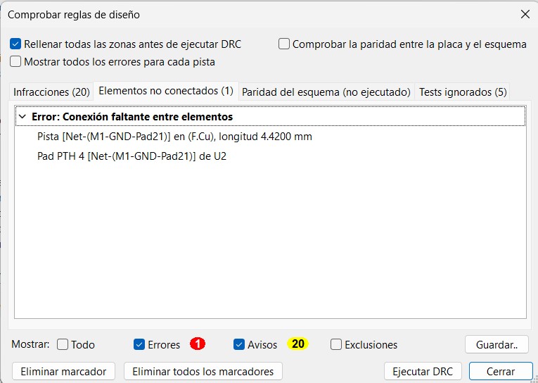
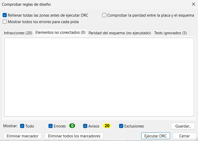
I ran the DRC and 20 warnings and one error appeared. The error was caused by an unconnected pin on the DHT22. According to the DHT22 datasheet, this pin is generally left unconnected. To eliminate the error, I connected that pin to ground(Although it is not recommended). In the following image, it can be seen that the error has been resolved.
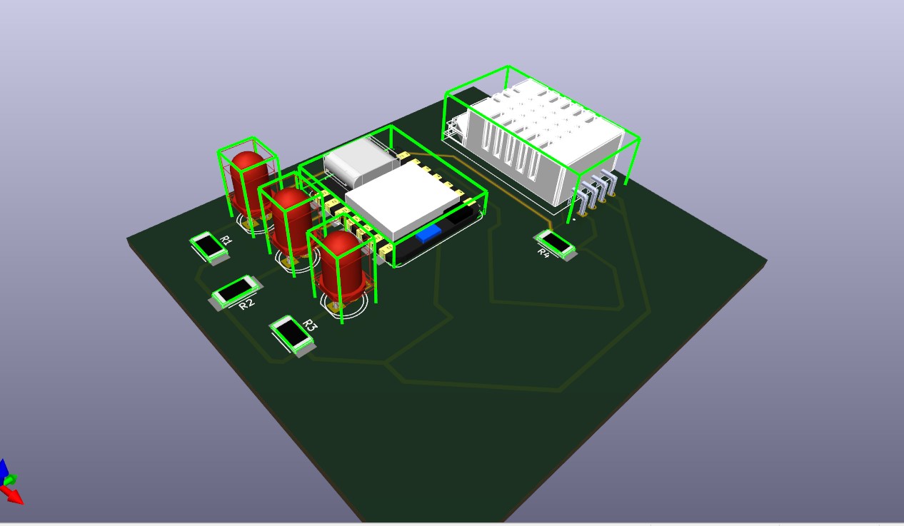
The final design would be as follows:
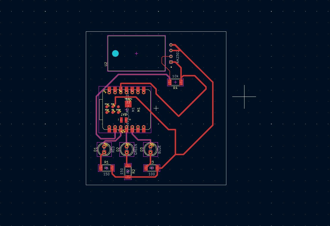
Result Final
No es mi mejor diseño es mi primera vez usando un software EDA espero fabricarlo la semana de producion de PCB pero lo importante es que lo hice yo mismo
What I Learned
During this week, I learned how to use an EDA tool like KiCad; it was my first time working with this type of software.
I learned how to design a PCB board from scratch, calculate the required resistors for the LEDs, and properly route the PCB traces.
Additionally, I learned how to verify my circuit using KiCad’s ERC and DRC tools to ensure there were no design errors.
During the process, I also learned that the DHT22 sensor requires a 5kΩ to 10kΩ pull-up resistor between the data (SDA) pin and VCC to ensure stable communication and improve reading accuracy.
Dowload File
Mission accomplished! 😊