Assignment
Group Assignment
We characterized the design rules for our in-house PCB production process.
We also submitted a PCB design to a board house.
Individual Assignment
I made and tested an embedded microcontroller system that I designed.
Introduction
Electronics production turns a circuit design into a physical board.
A PCB is stronger and cleaner than a breadboard.
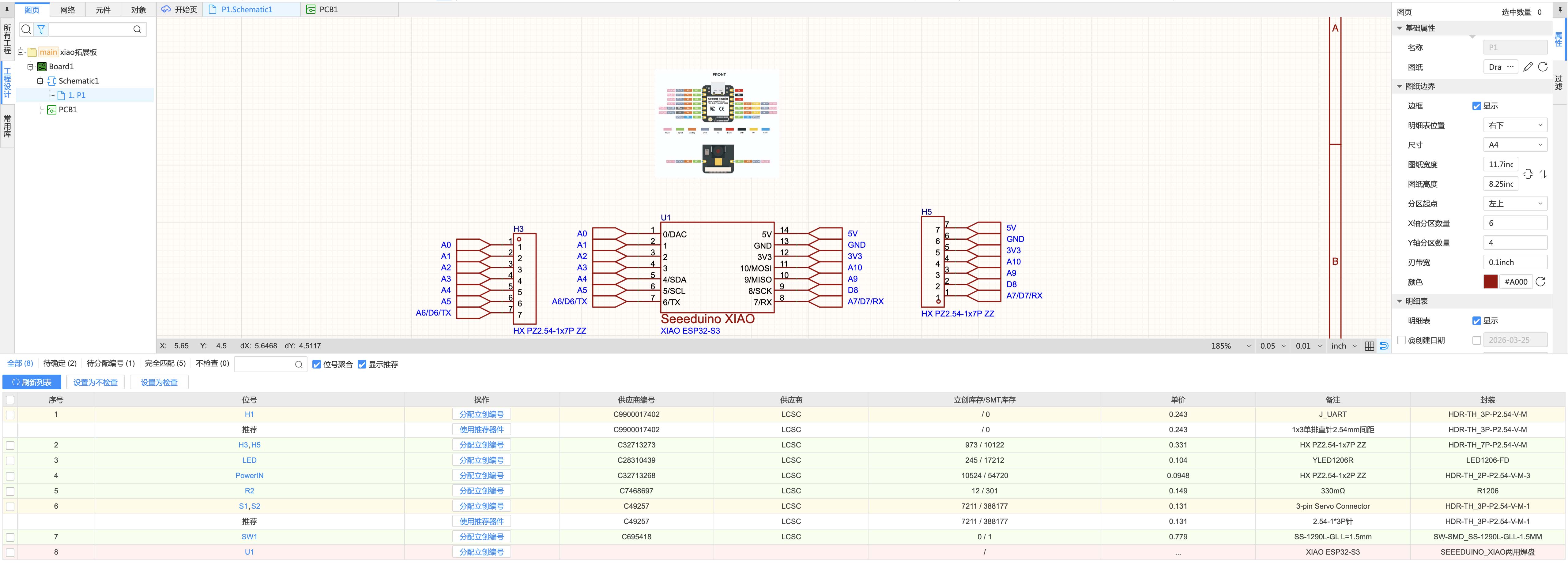
I designed a small development board for the XIAO ESP32C3.
The board includes an LED, switch, headers, servo connectors, and power input.
Why I Used LCEDA-Pro and JLCPCB
I used KiCad in Week 06 to learn basic PCB design.
For this week, I used LCEDA-Pro because it links directly with JLCPCB.
This made component sourcing, BOM checking, and board-house submission faster in China.
LCEDA-Pro also connects components with the LCSC library.
This helped me check symbols, footprints, stock, and prices during the design process.
Process Overview
I organized this week as one complete PCB production workflow.
- Understand the PCB material, machine, and tool limits.
- Test design rules with the group.
- Design the schematic and PCB layout.
- Check the BOM, DRC, and board-house submission.
- Prepare the toolpath, workholding, and machine setup.
- Mill the PCB and inspect the result.
- Remove burrs before soldering components.
- Solder, test continuity, program, and debug the board.
Material, Tools, and Machine
PCB Material
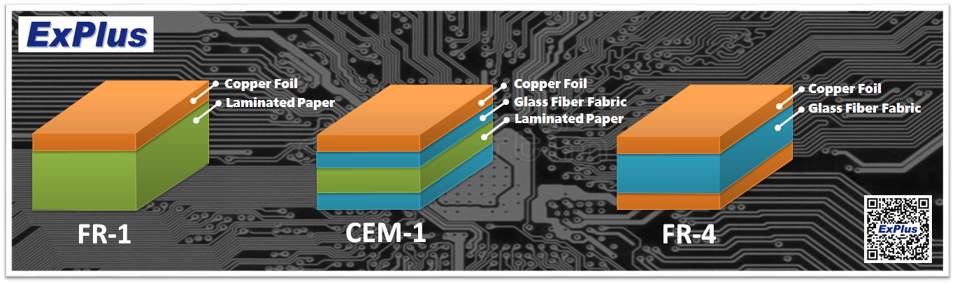
The PCB blank looked like FR4 copper-clad laminate.
FR4 is a rigid glass-fiber epoxy PCB material.
It is harder than soft copper-clad paper boards.
It can wear small milling tools faster.
It can also create fine fiberglass dust during milling.
I cleaned the board and machine area after milling.
I compared FR-1 and FR-4 to understand the material difference.
FR-1 uses copper foil with laminated paper.
FR-4 uses copper foil with glass fiber fabric.
My board used FR4, so dust control was important during milling.
Machine, Tool, and Software
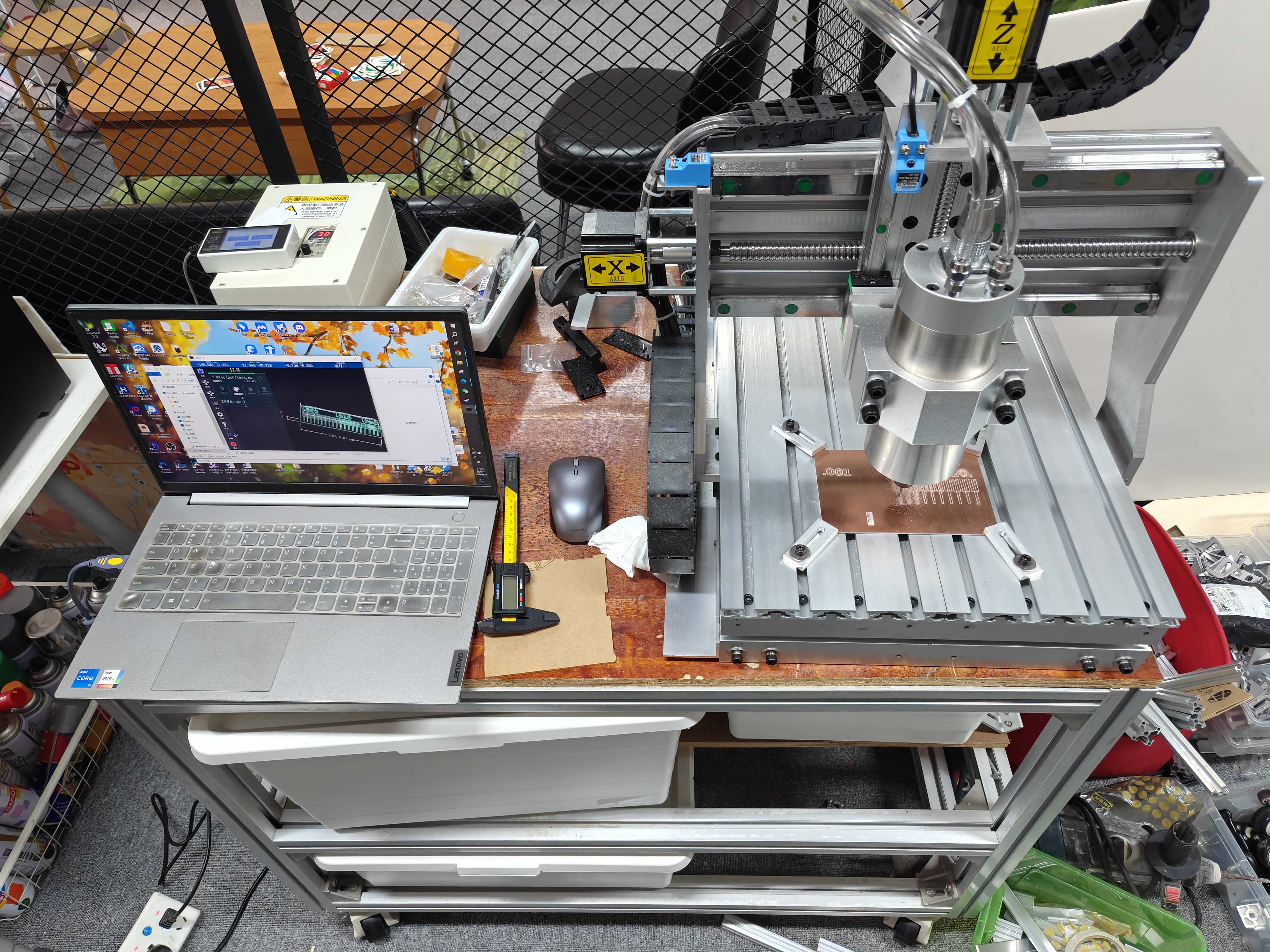
I used our in-house CNC PCB milling machine.
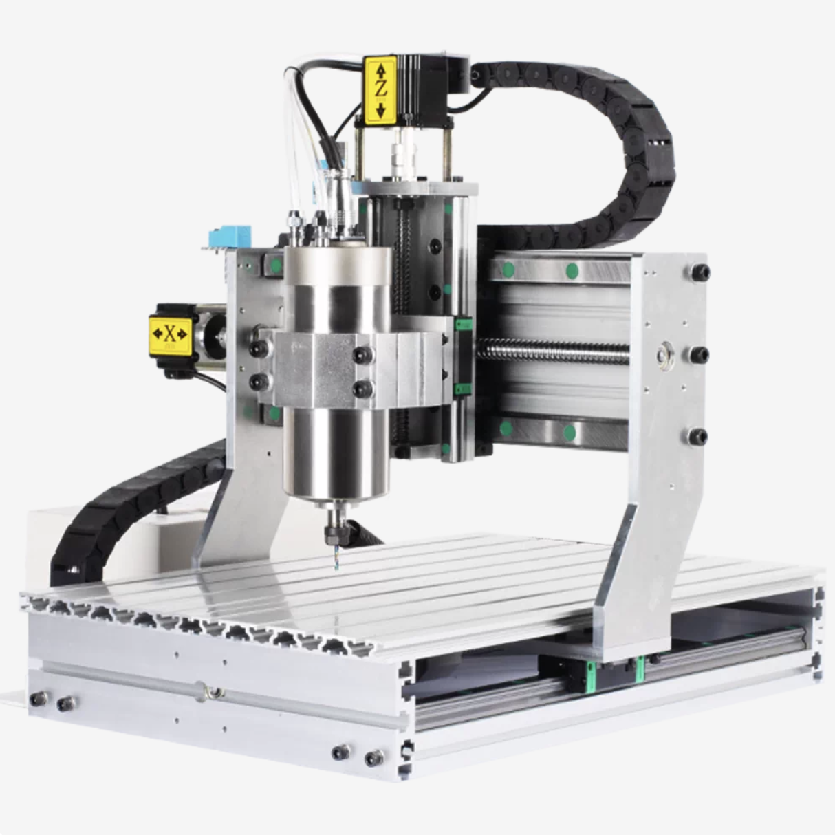
CNC Machine Parameters
I recorded the main machine parameters in English instead of using a Chinese screenshot.
| Item | Value |
|---|---|
| Machine model | M3040-1500 desktop CNC milling machine |
| Spindle power | 1.5 kW water-cooled spindle |
| Power input | 220 V |
| Maximum spindle speed | 24000 rpm |
| Working travel | About X285 × Y414 × Z92 mm |
| Positioning accuracy | 0.01 mm |
| Control method | USB controller and CNCV4 workflow |
The machine can engrave PCB, wood, acrylic, plastic, and soft metal.
I used it only for PCB milling in this assignment.
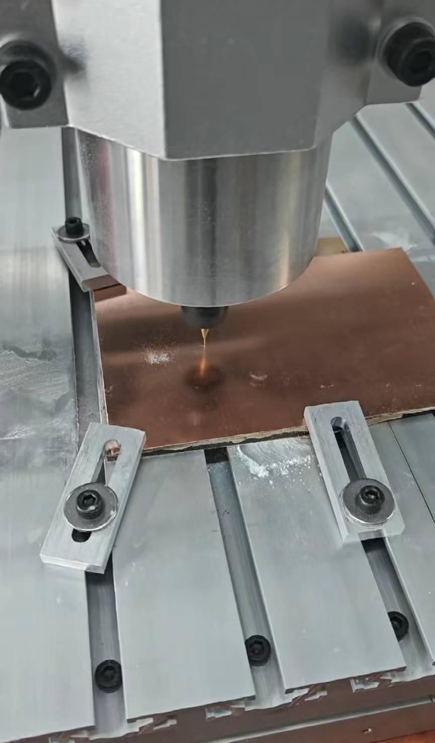
The machine removes copper around traces.
This creates electrical isolation between PCB pads and routes.
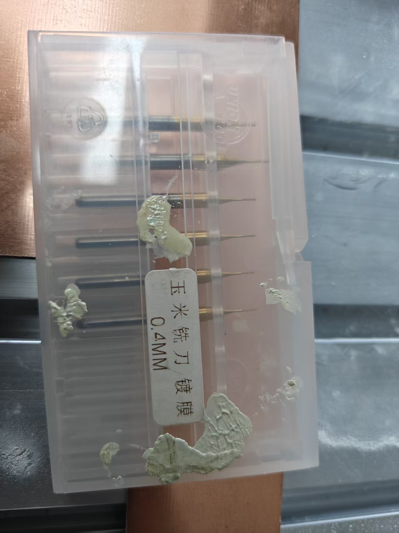
I used small PCB milling bits for trace isolation and cutting.
The tool tip must be clean, sharp, and correctly fixed.
A dull tool can leave heavy burrs on the copper.
I used JDpaint to prepare the PCB milling toolpath.
I used JDSimu to preview the toolpath before milling.
I used CNCV4 to load the NC files and run the machine.
- CNC PCB milling machine
- Small engraving bit and 0.4 mm milling bit
- FR4 copper-clad board
- Metal edge clamps
- JDpaint for toolpath preparation
- JDSimu for toolpath simulation
- CNCV4 for machine control
- Multimeter for checking continuity
- Soldering iron for assembly
Group Assignment
Design Rule Test
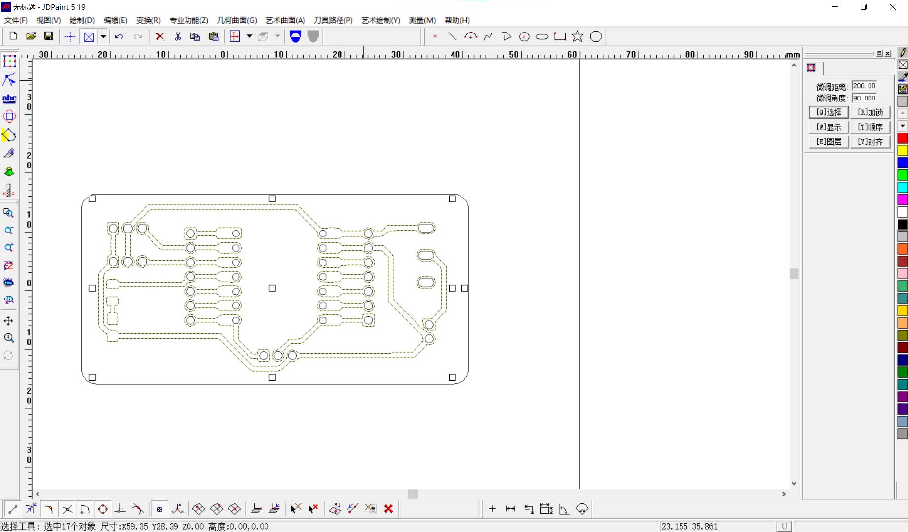
We tested the design rules of our PCB milling process.
The test pattern used different trace widths and clearances.

This test helped us understand the real machine limits.
Milling Settings
We set the engraving range and cutting depth before milling.
The machine setting screenshot was in Chinese.
I restated the key settings in English below.
| Setting | Recorded Value | Purpose |
|---|---|---|
| Spindle speed | 24000 rpm | Keeps the small tool cutting smoothly. |
| Feed value | 0.600 in the software | Controls how fast the tool moves. |
| Cutting depth | 0.500 mm in the group test | Cuts through copper for isolation testing. |
| Toolpath direction | Outward offset | Keeps the cut outside the selected shape. |
Group Result
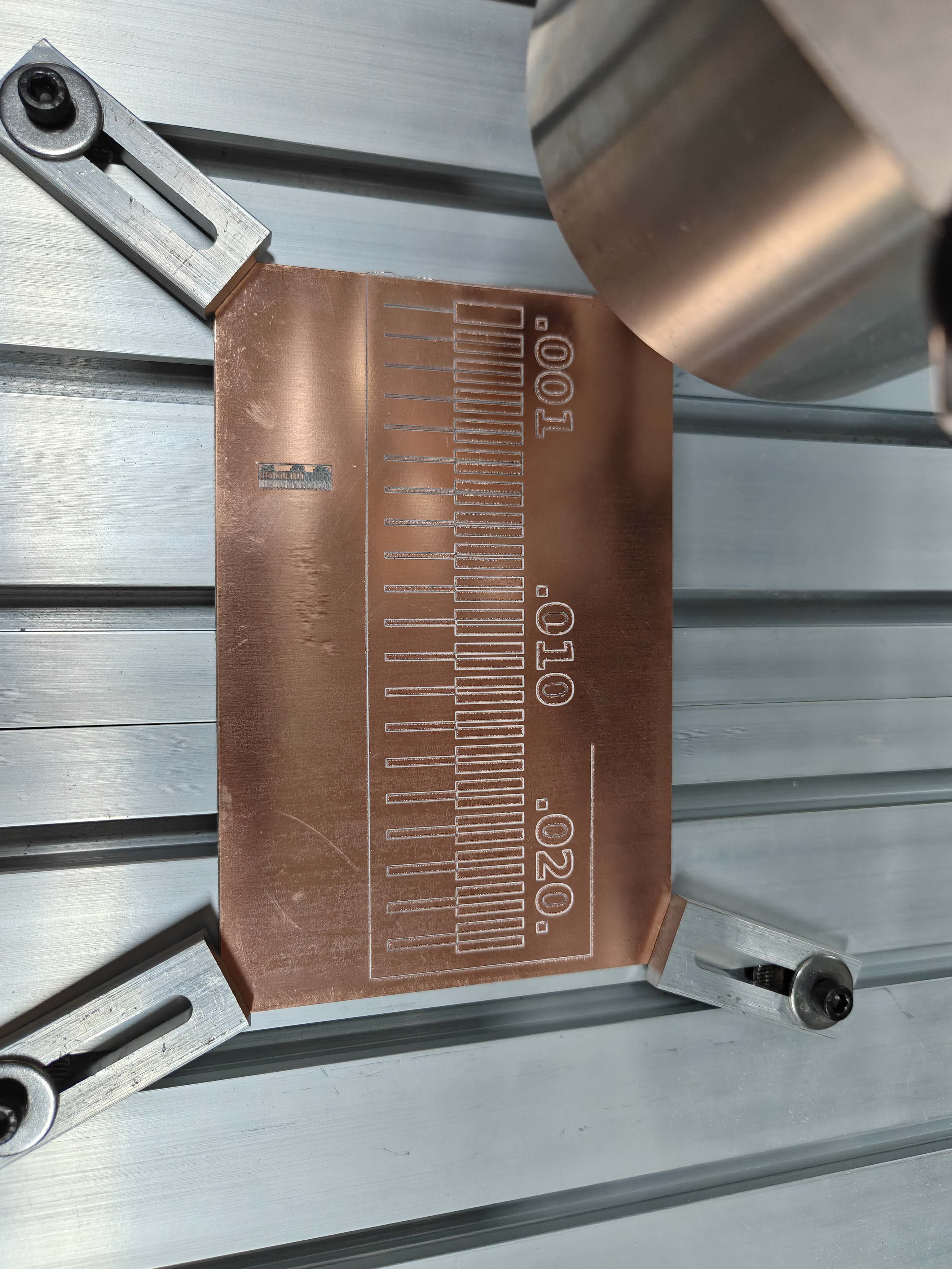
Wider traces and clearances were more reliable.
Very thin traces were fragile and harder to isolate cleanly.
I used this result as a reference for my own board.
The board-house submission is documented after the PCB layout section.
Individual Assignment
Board Concept
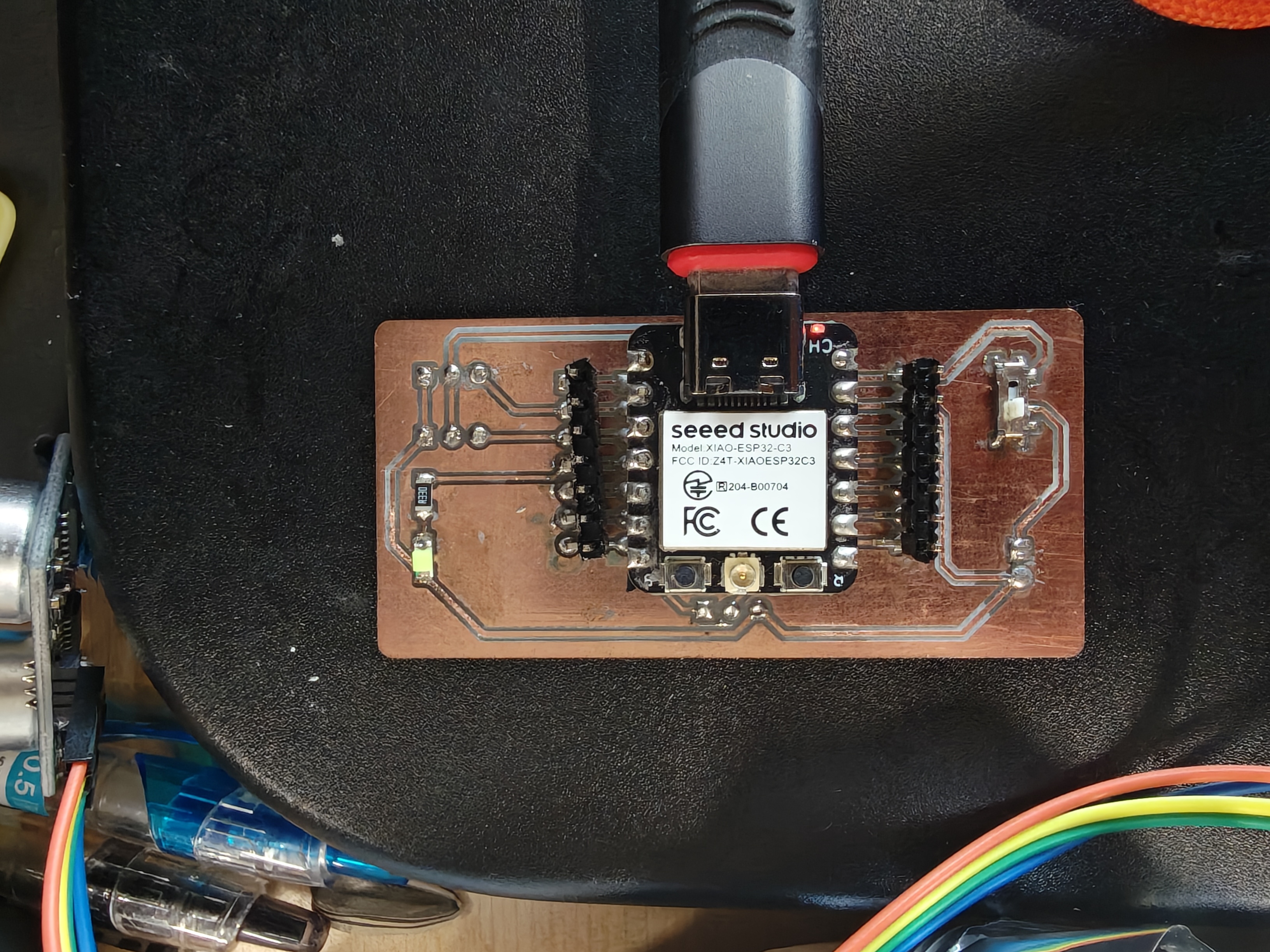
I designed a compact XIAO ESP32C3 development board.
It supports LED testing, servo output, serial communication, and external power.
- XIAO ESP32C3 microcontroller module
- LED output tested as D3 in Arduino
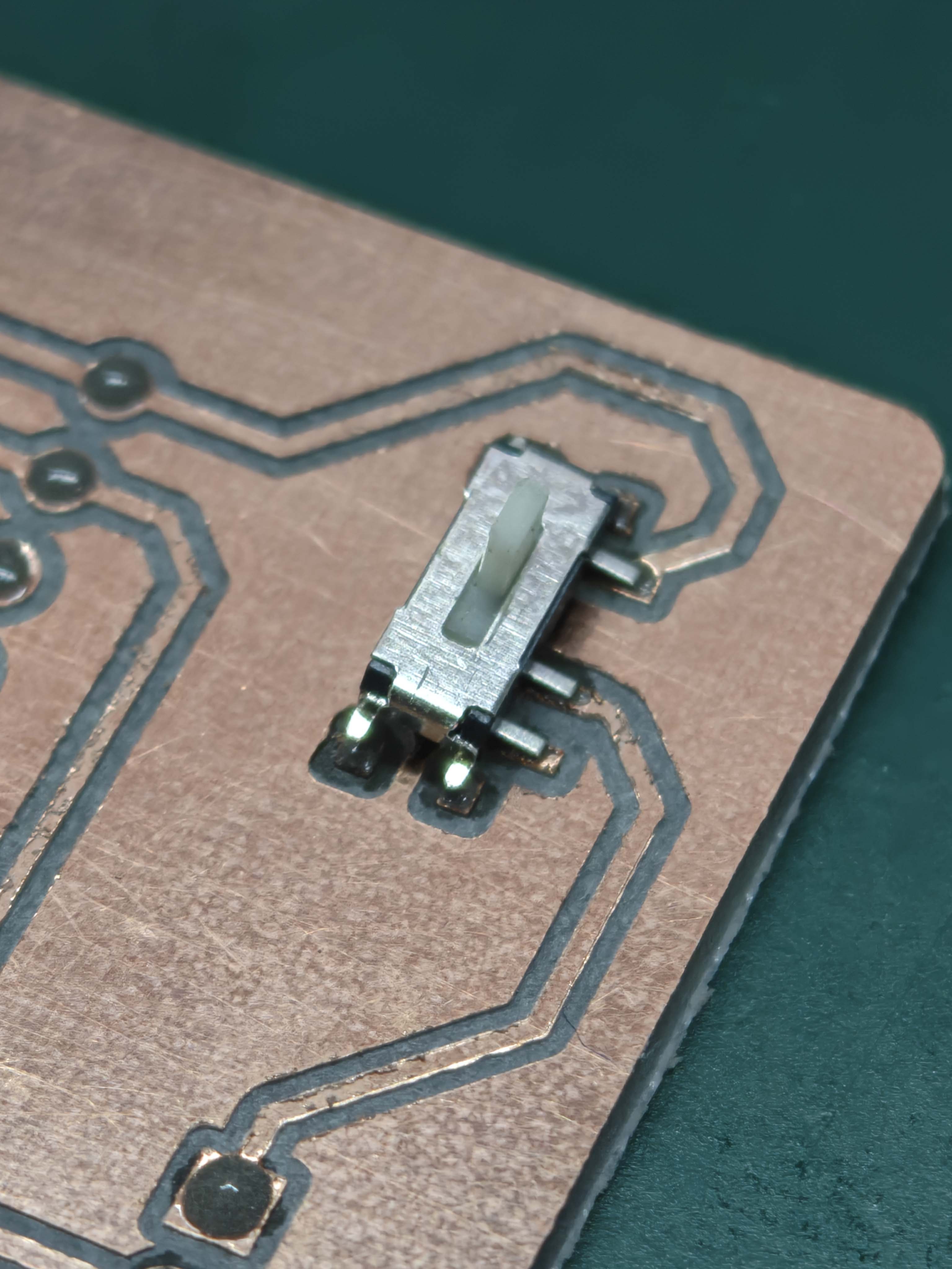
- Slide switch on the power line
- Two 3-pin servo connectors
- TX, RX, and GND serial header
- 5V external power input
- 5V, 3V3, and GND headers
Schematic Design
I designed the schematic in LCEDA-Pro.
The XIAO ESP32C3 was the main microcontroller.
I added headers, servo connectors, a switch, power input, and an LED circuit.
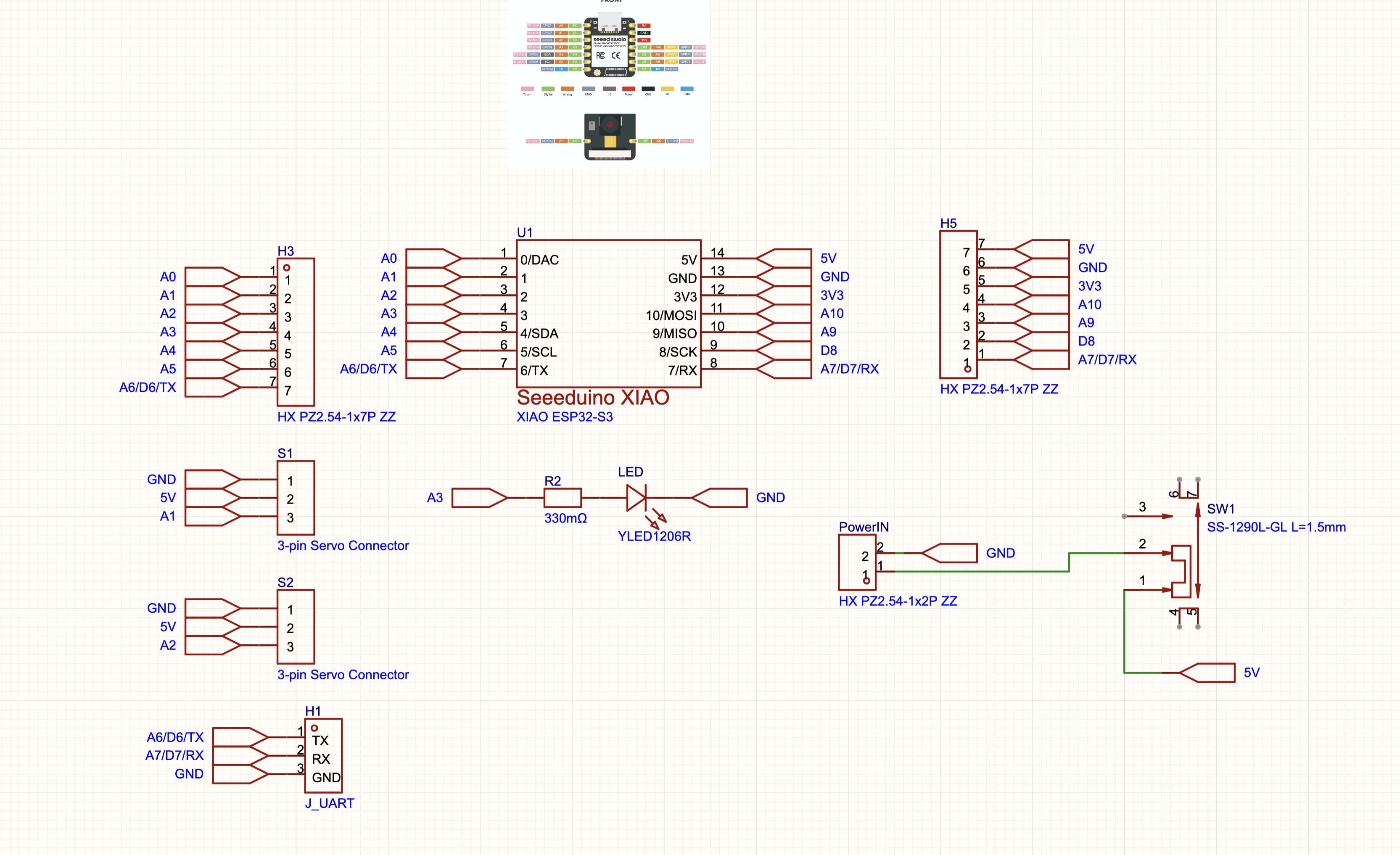
The schematic label was A3, but Arduino IDE used D3.
I used D3 in the final test code.
BOM and Component Source
I checked the bill of materials in LCEDA-Pro.
Most components were selected from LCSC.
The BOM helped me check packages, stock, supplier numbers, and prices.
Estimated BOM Cost
This estimate only includes peripheral components.
It excludes PCB fabrication, shipping, and the XIAO ESP32C3 module.
| Designator | Component | Quantity | Unit Price (RMB) | Subtotal (RMB) |
|---|---|---|---|---|
| H1 | 1x3 pin header | 1 | 0.243 | 0.243 |
| H3, H5 | 1x7 pin header | 2 | 0.331 | 0.662 |
| LED | SMD LED | 1 | 0.104 | 0.104 |
| PowerIN | 2-pin power connector | 1 | 0.0948 | 0.0948 |
| R2 | SMD resistor | 1 | 0.149 | 0.149 |
| S1, S2 | 3-pin servo connector | 2 | 0.131 | 0.262 |
| SW1 | SMD slide switch | 1 | 0.779 | 0.779 |
| U1 | XIAO ESP32C3 module | 1 | Not included | Not included |
| Total peripheral component cost | 2.29 | |||
The peripheral components cost about RMB 2.29.
The PCB was prepared through JLCPCB in China.
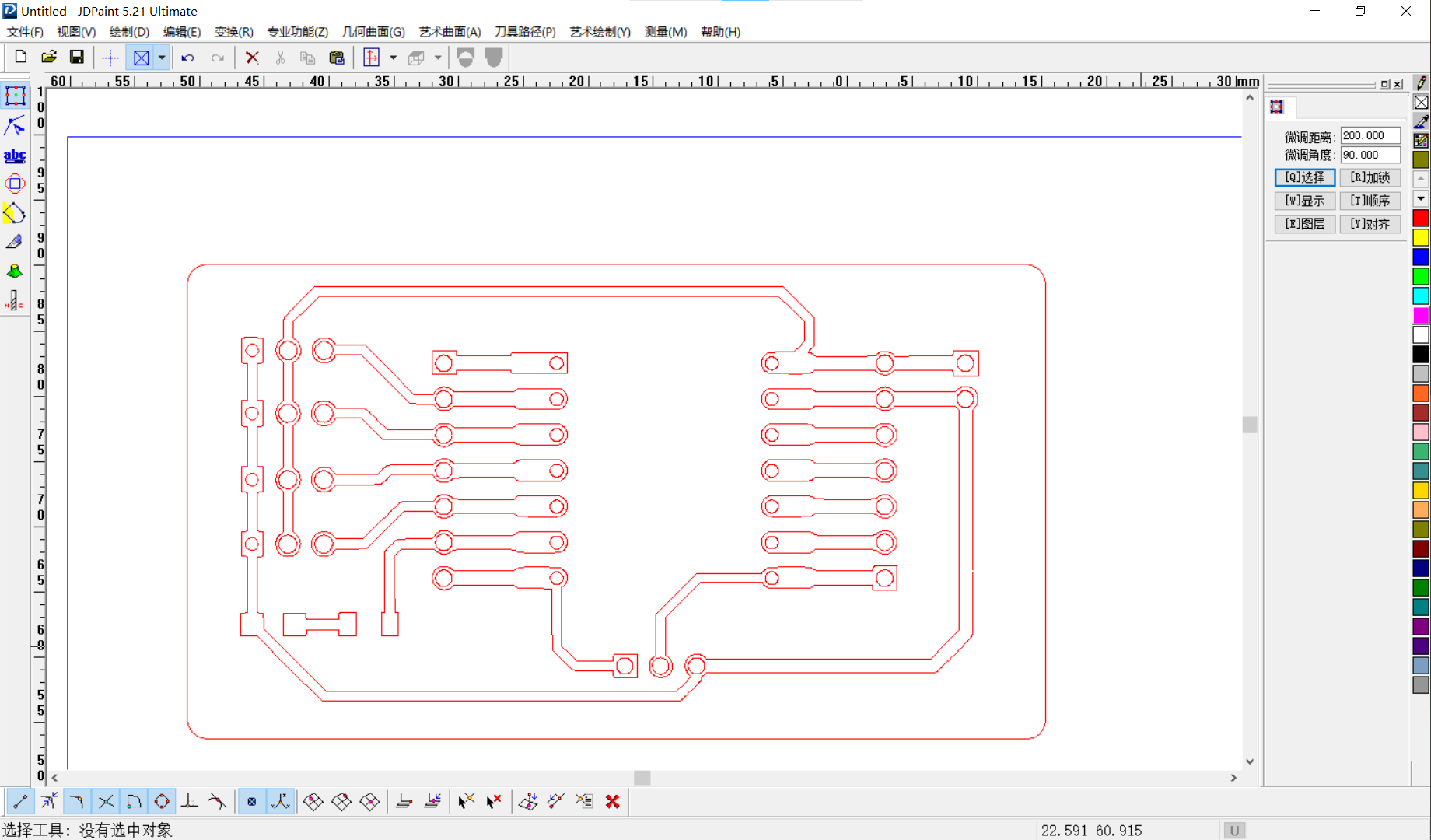
PCB Layout and DRC
After the schematic, I moved to PCB layout.
I placed the XIAO module near the center of the board.
The LED and resistor were placed on the left side.
The switch and power input were placed on the right side.
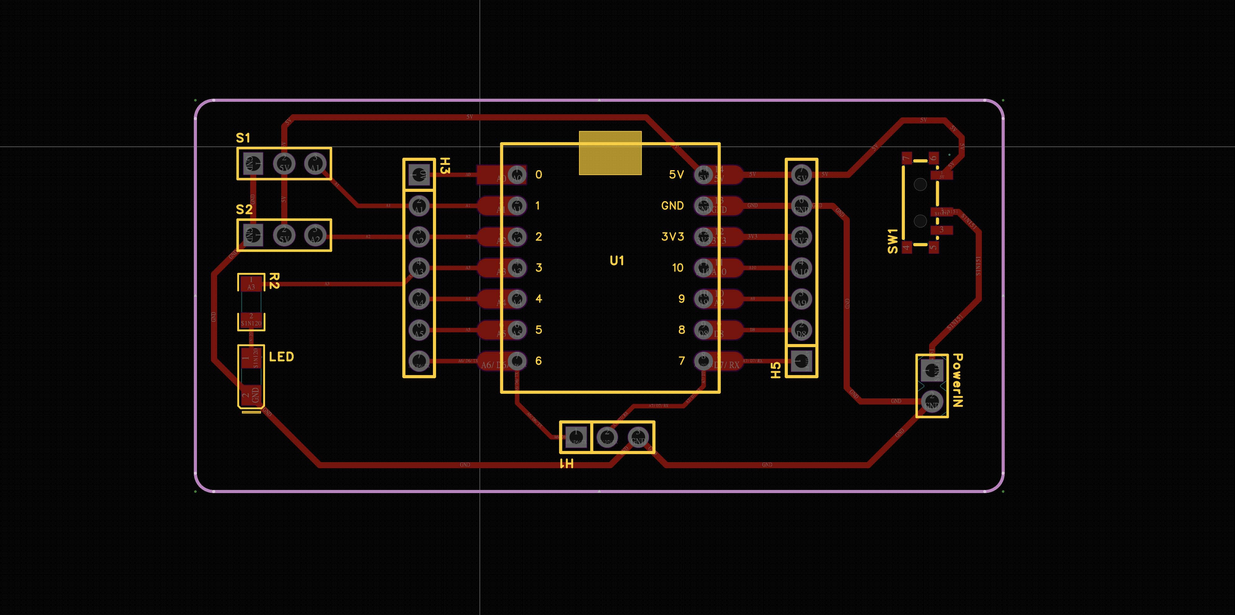
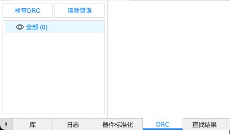
I ran DRC before fabrication.
The result showed zero detected errors.
Board House Submission
After DRC, I tested the board-house submission workflow.
LCEDA-Pro connects directly with JLCPCB for layout orders.
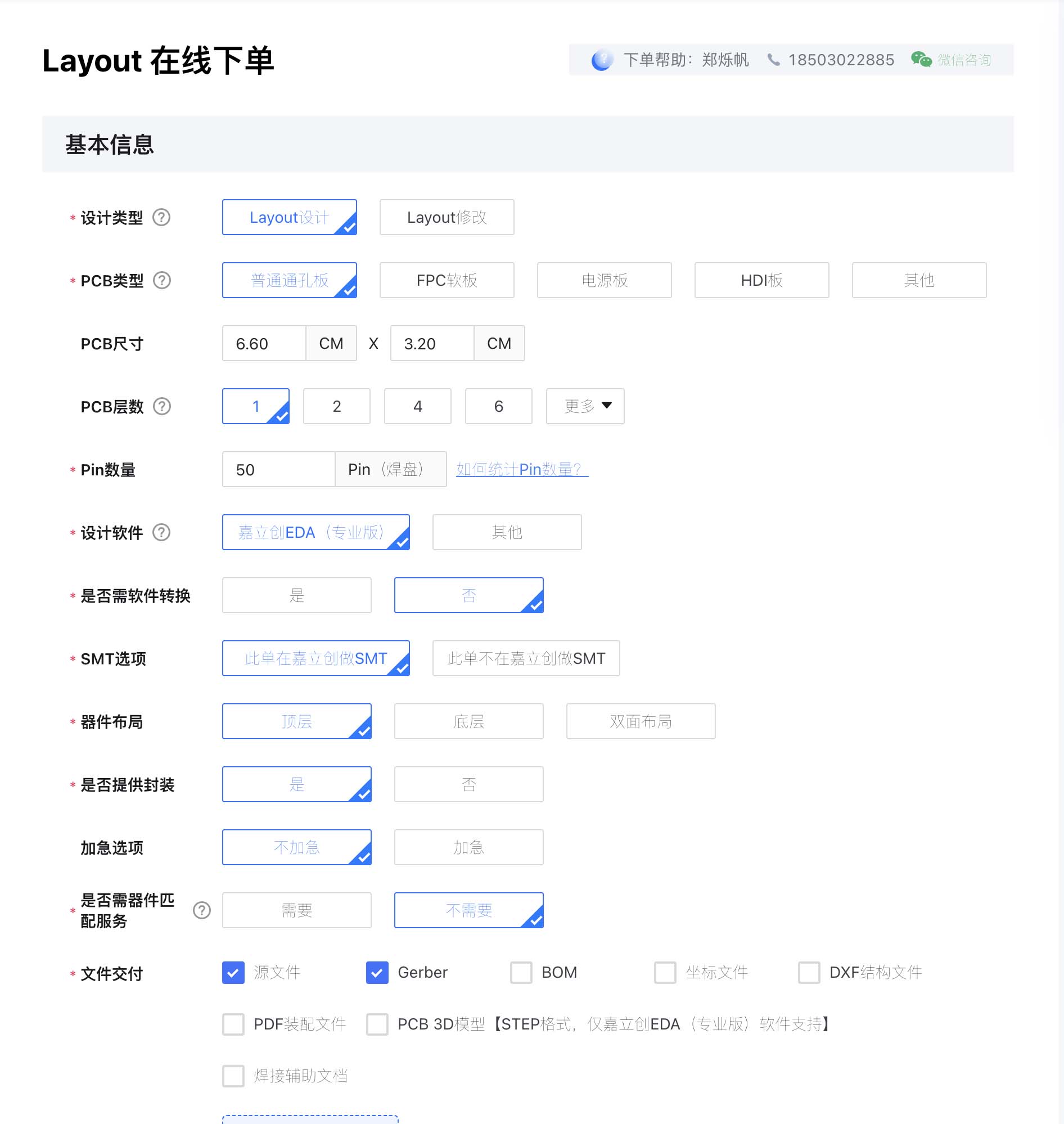
This checked the board size, layer number, pin count, and Gerber file.
I did not complete payment for this assignment.
PCB Fabrication and Machine Setup
Workholding and Safety
The PCB must stay flat during milling.
A loose board can break the tool.
It can also damage traces or clamps.
Some earlier photos show a spoilboard under the copper board.
I learned that this setup needs extra care.
A loose spoilboard under metal jigs can be unsafe.
The underlay can move or change the Z height.
Metal clamps must stay outside the toolpath.
The PCB should be pressed evenly and checked by hand.
This setup fixed the board from the edges.
I checked the toolpath before starting the cut.
After cutting, I stopped the machine first.
Then I removed the clamps and detached the board by hand.
Machine Start and Emergency Stop
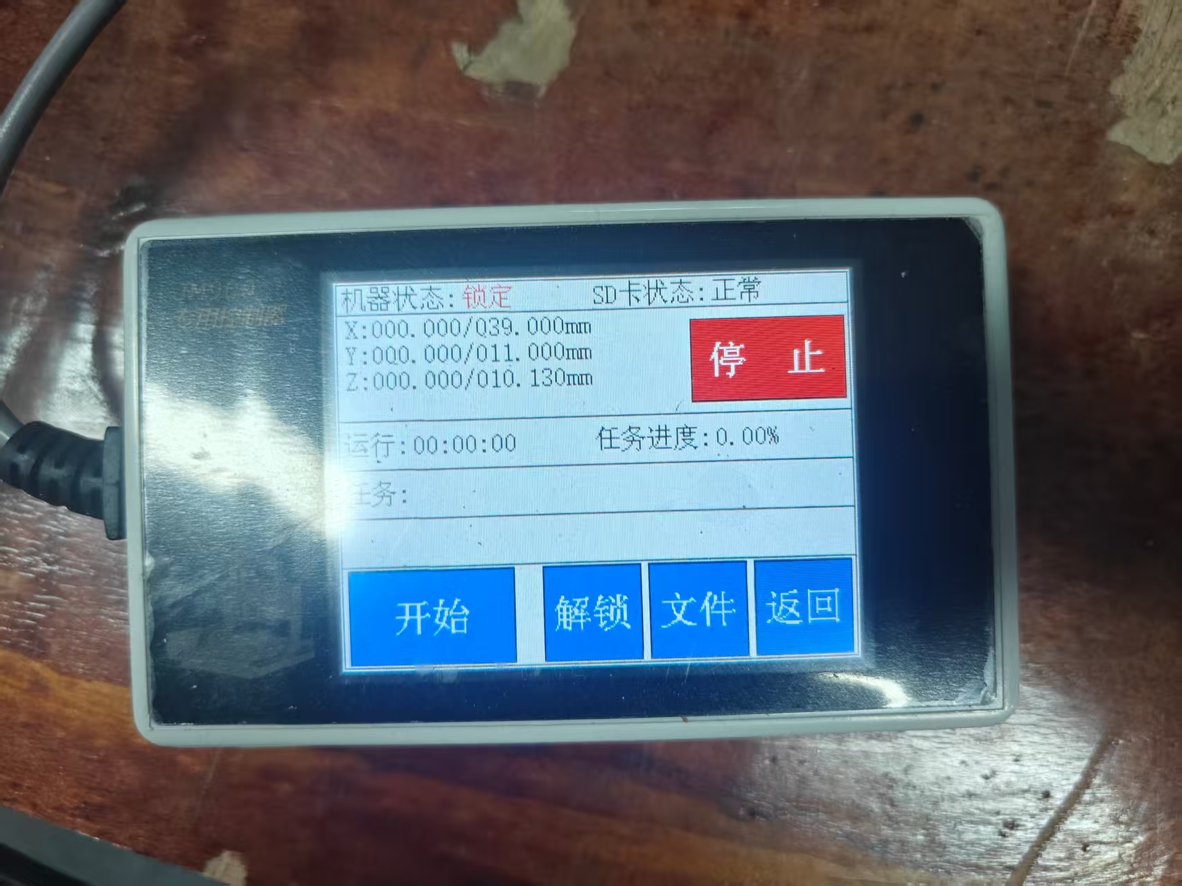
I turned on the main power and checked the controller screen.
I loaded the NC file after setting X, Y, and Z zero.
I pressed Start only after checking the toolpath preview.
If the tool hits the clamp, I must press the red Stop button.
I also stop the machine if there is abnormal noise or vibration.
I wait until the spindle fully stops before touching the board.
Machine Setup Workflow
- Clean the machine bed and PCB surface.
- Place the PCB on a flat support.
- Fix the board with edge clamps.
- Keep all clamps outside the cutting path.
- Install the engraving bit in the collet.
- Check that the bit is not loose.
- Set the X and Y origin on the board.
- Lower the tool slowly for Z zero.
- Preview the toolpath before starting the cut.
- Watch the first cut carefully.
Software Screens and English Translation
Some machine screenshots were in Chinese.
I translated the important machining settings below.
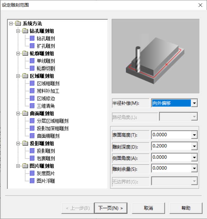
This screen sets the engraving area for PCB trace isolation.
Radius compensation means tool radius offset.
I used outward offset for the trace path.
The surface height was 0.000 mm.
The engraving depth was 0.200 mm.
This screen shows the cut-out setting.
I used this path to separate the PCB from the blank.
The cut-out depth was set to 1.600 mm.
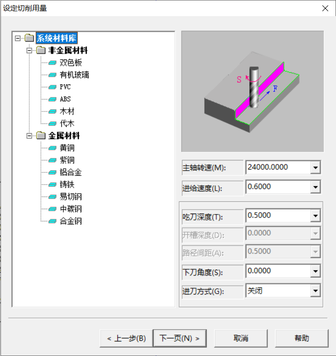
This screen shows the main cutting parameters.
The spindle speed was set to 24000 rpm.
The feed value was set to 0.600 in the software.
The cutting depth was set to 0.500 mm.
The path spacing was set to 0.500 mm.
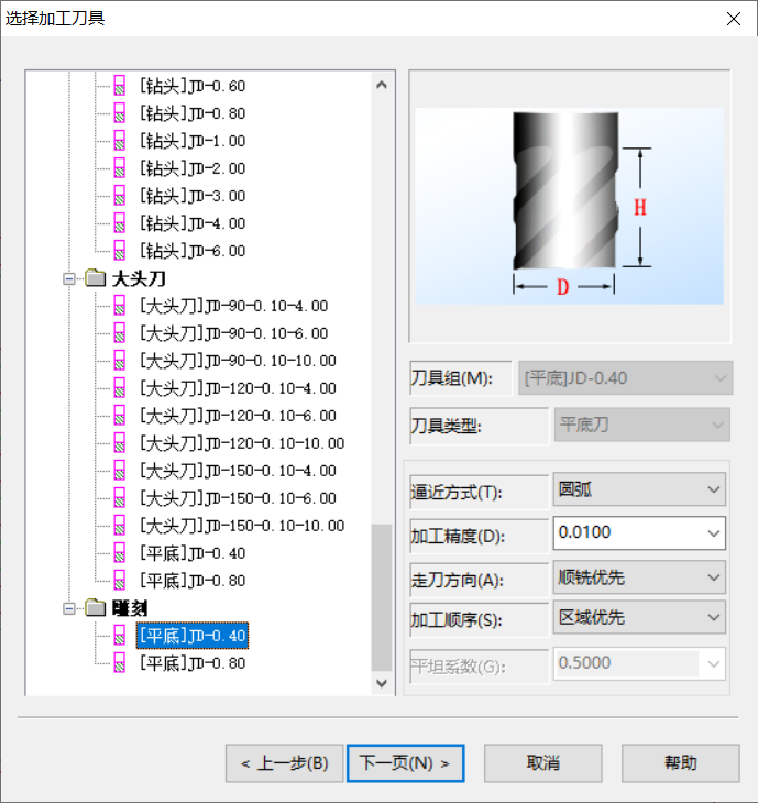
This screen shows the machining tool selection.
I selected a 0.4 mm flat end mill in JDpaint.
The machining accuracy was set to 0.0100.
The toolpath direction used climb milling priority.
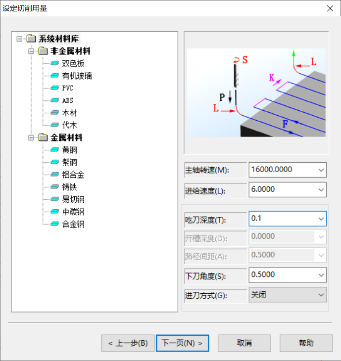
This screen records another cutting setup I checked.
The spindle speed was 16000 rpm.
The feed value was 6.0000 in the software.
The cutting depth was 0.1 mm.
I compared these values before generating the toolpath.
Machining Settings Summary
| Item | Setting | Purpose |
|---|---|---|
| Material | FR4 copper-clad board | Rigid PCB base with copper surface. |
| Trace tool | Small engraving bit | Removes copper around traces. |
| Selected tool | 0.4 mm flat end mill | Used for fine PCB milling paths. |
| Trace depth | 0.200 mm | Cuts copper isolation paths. |
| Cut-out depth | 1.600 mm | Separates the PCB from the blank. |
| Main spindle speed | 24000 rpm | Provides high speed for small cuts. |
| Main feed value | 0.600 in the software | Controls tool movement speed. |
| Toolpath compensation | Outward offset | Keeps the cut outside the selected shape. |
Toolpath Preview and Machine Control
I checked the trace paths and board outline before exporting NC files.
This helped confirm that the toolpath avoided the metal clamps.
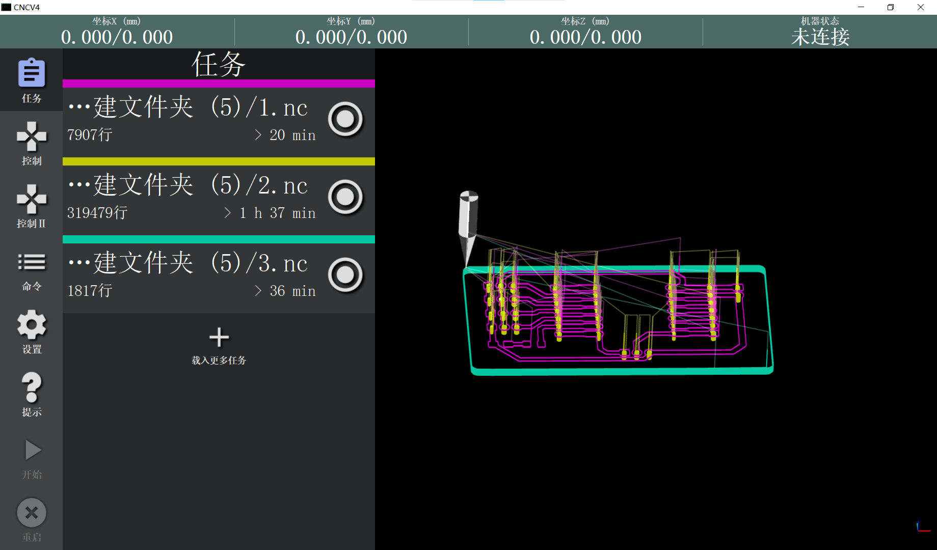
I loaded the NC files into CNCV4.
I checked the tool position before starting the milling job.
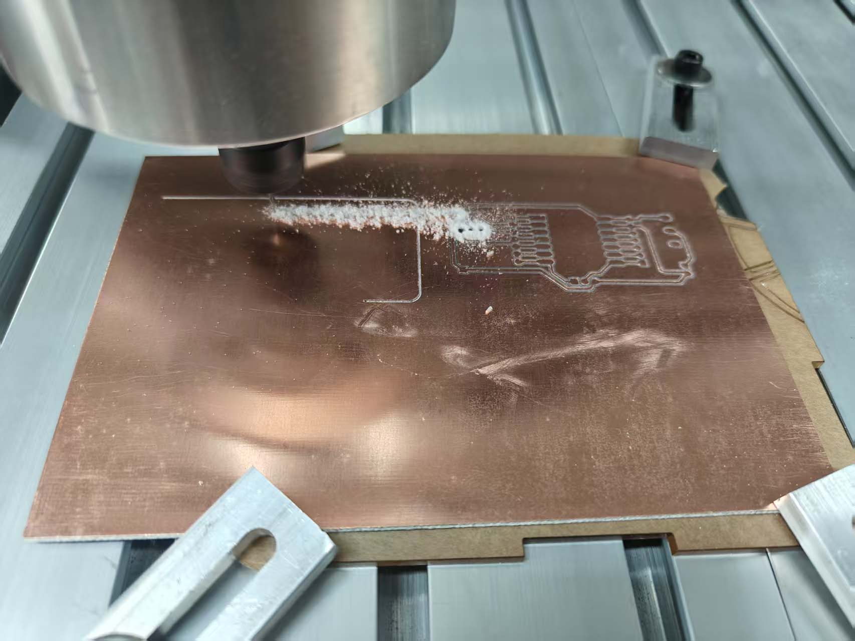
Milling Process
I prepared the milling file after finishing the PCB layout.
The copper board was fixed firmly to the machine bed.
I zeroed the tool carefully before cutting.
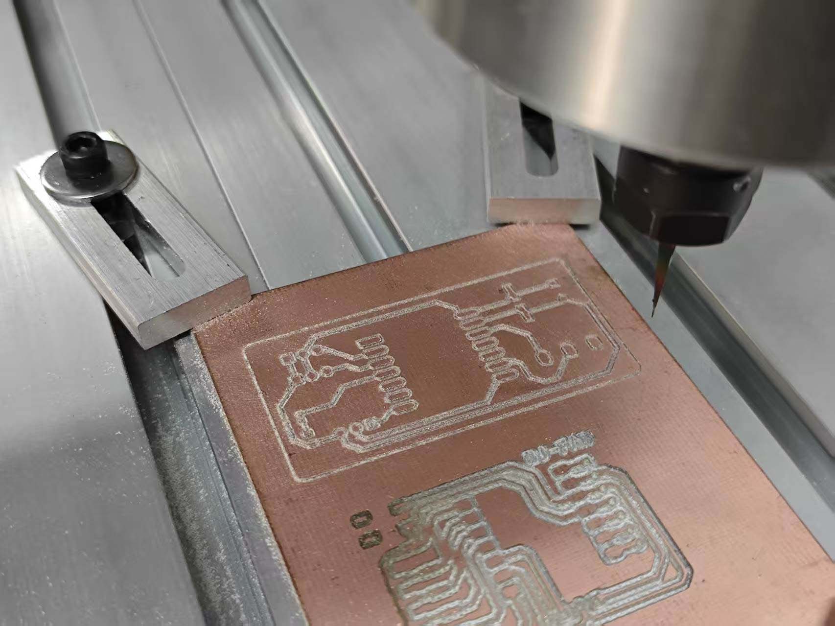
Milling quality depended on cutting depth and board flatness.
A shallow cut did not isolate the copper fully.
A deep cut made some traces rough.
Post-processing Before Soldering
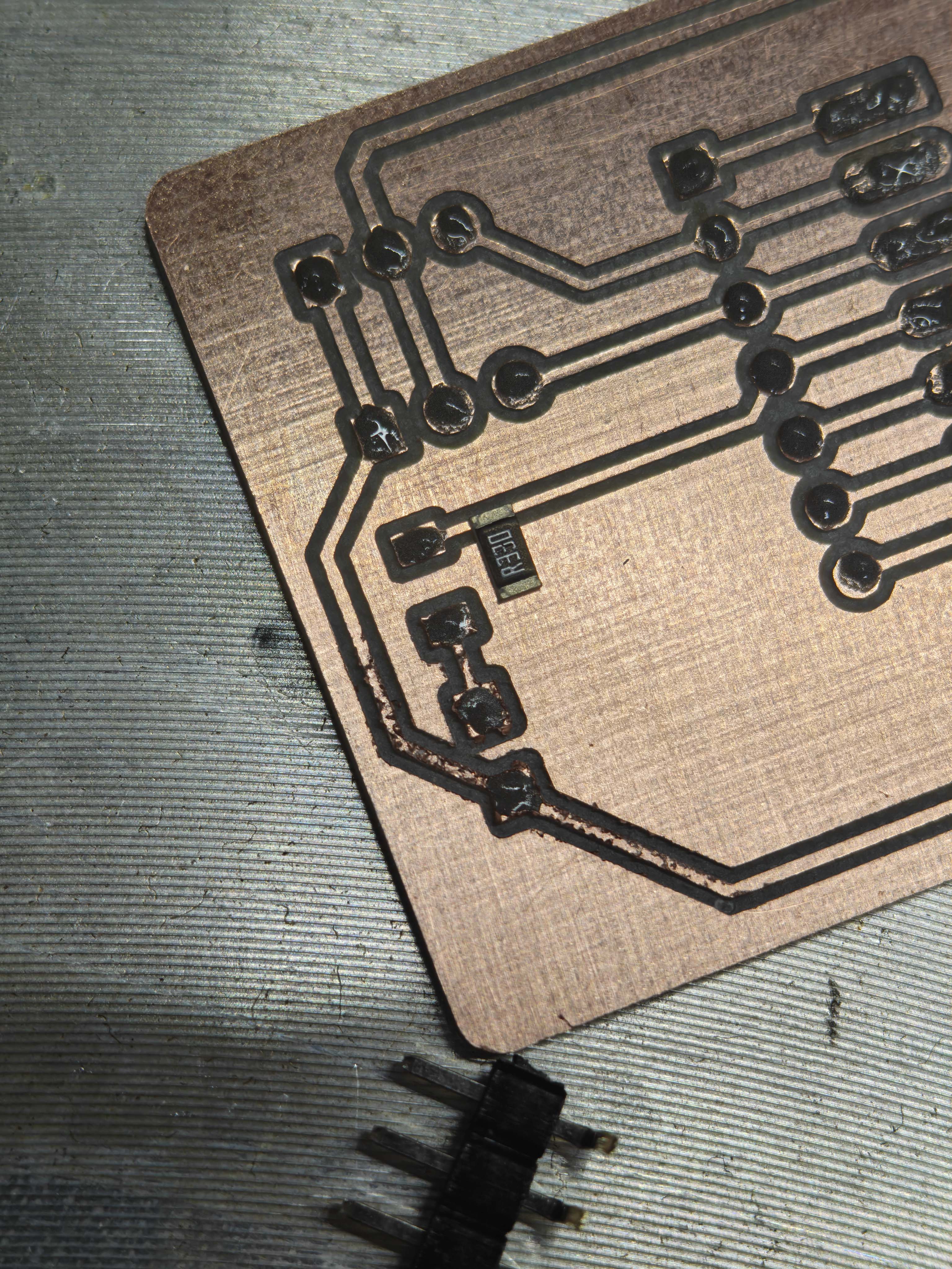
The milled board showed visible burrs around some traces.
This was not an acceptable final surface.
Burrs can cause weak joints or short circuits.
They can also hide small broken traces.
I inspected the board before soldering components.
I removed loose burrs with a blade and brush.
I then cleaned the copper dust from the board.
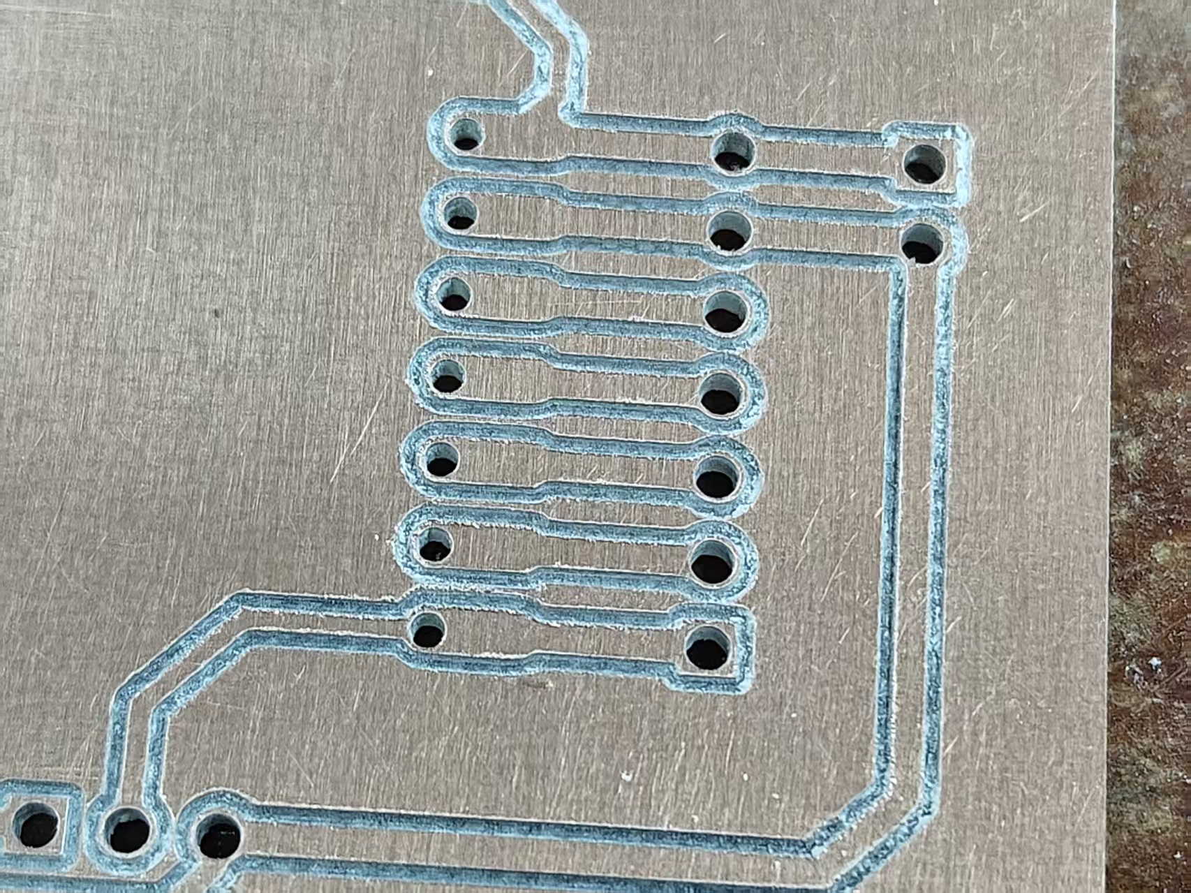
I checked the cleaned traces with a multimeter.
This step reduced the risk of solder bridges.
It also made the soldering area easier to inspect.
Manufacturing Issues and Corrections
Some milled traces were not clean enough before post-processing.
I used this as a learning point for setup quality.
The burrs could come from setup, copper quality, tool wear, or missing cleanup.
| Issue | Possible Cause | Correction |
|---|---|---|
| Burrs around traces | Depth, FR4, copper, or tool wear | Deburr and inspect before soldering. |
| Uneven isolation | Board flatness or Z-zero error | Check flatness and reset Z zero. |
| Unsafe support risk | Loose spoilboard under metal jigs | Use fixed support and safe clamps. |
| Rough copper edges | Dull tool or aggressive depth | Use a sharp bit and lighter passes. |
| Toolpath risk | Clamp too close to the cutting path | Preview the path before machining. |
Soldering and Assembly
I assembled the board after deburring and cleaning.
I did not solder components onto the rough milled surface.
The resistor, LED, and slide switch were SMD components.
These parts required careful alignment and inspection.
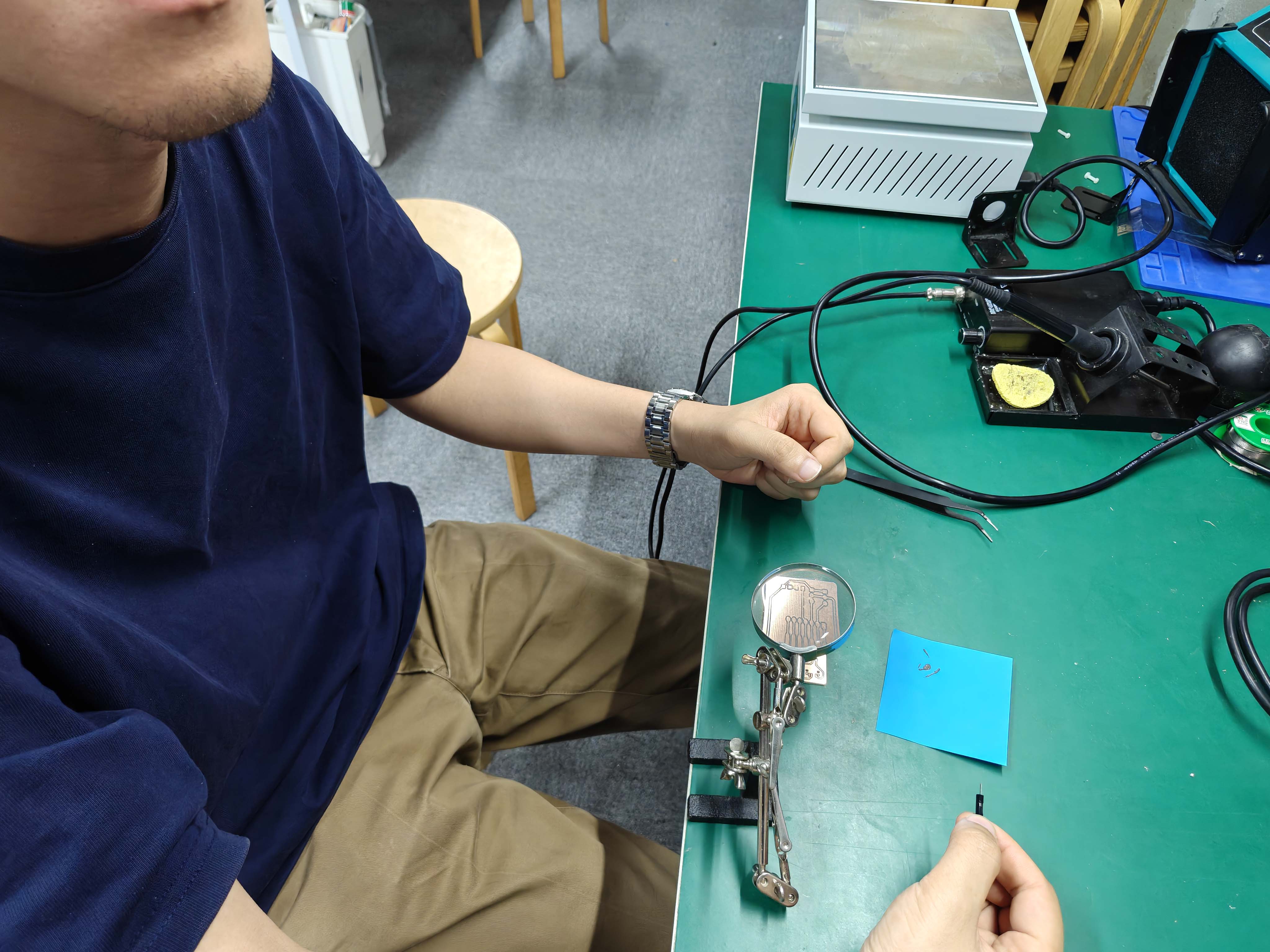
I checked the board for bridges, cold joints, and wrong orientation.
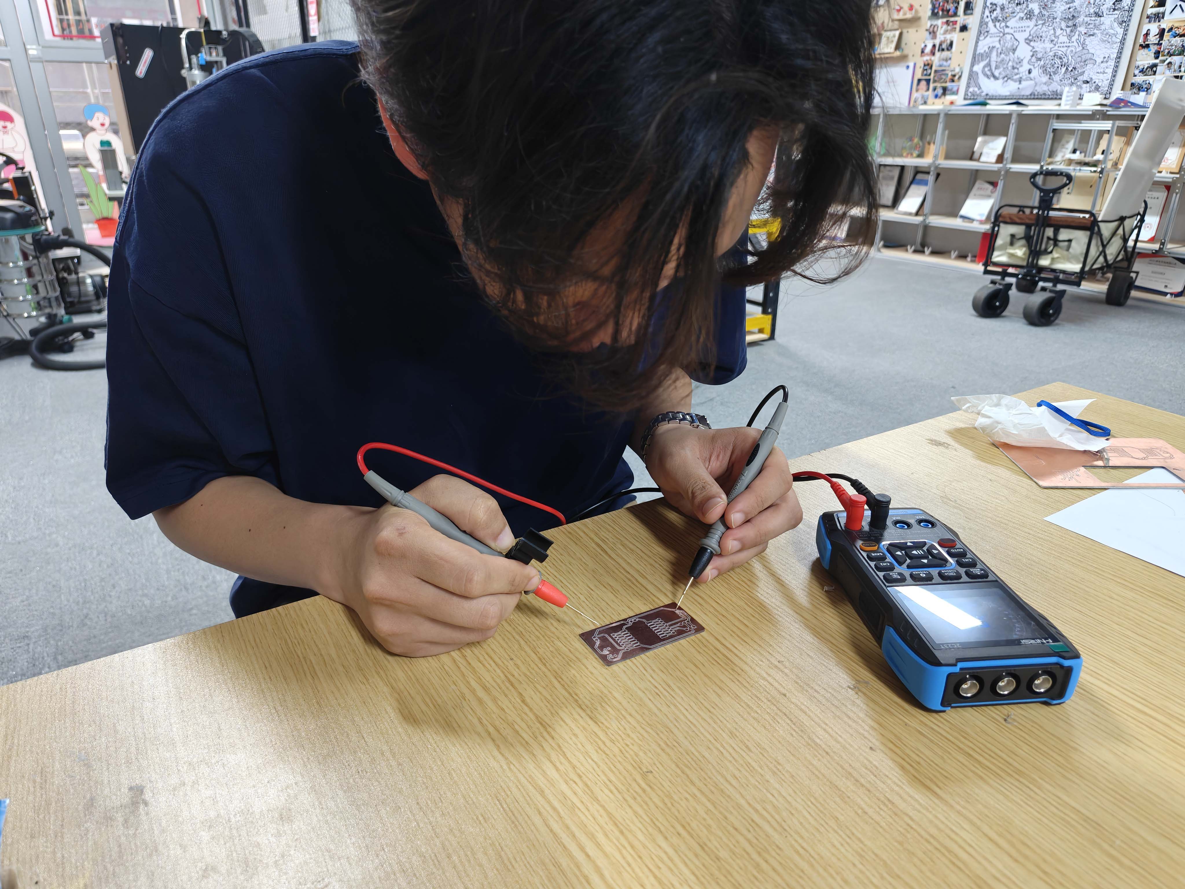
Continuity Test
I used a multimeter before powering the board.
This helped me check traces, pads, and possible short circuits.
Programming the Board
I programmed the board with Arduino IDE.
I selected XIAO ESP32C3 as the target board.
I also selected the correct serial port.
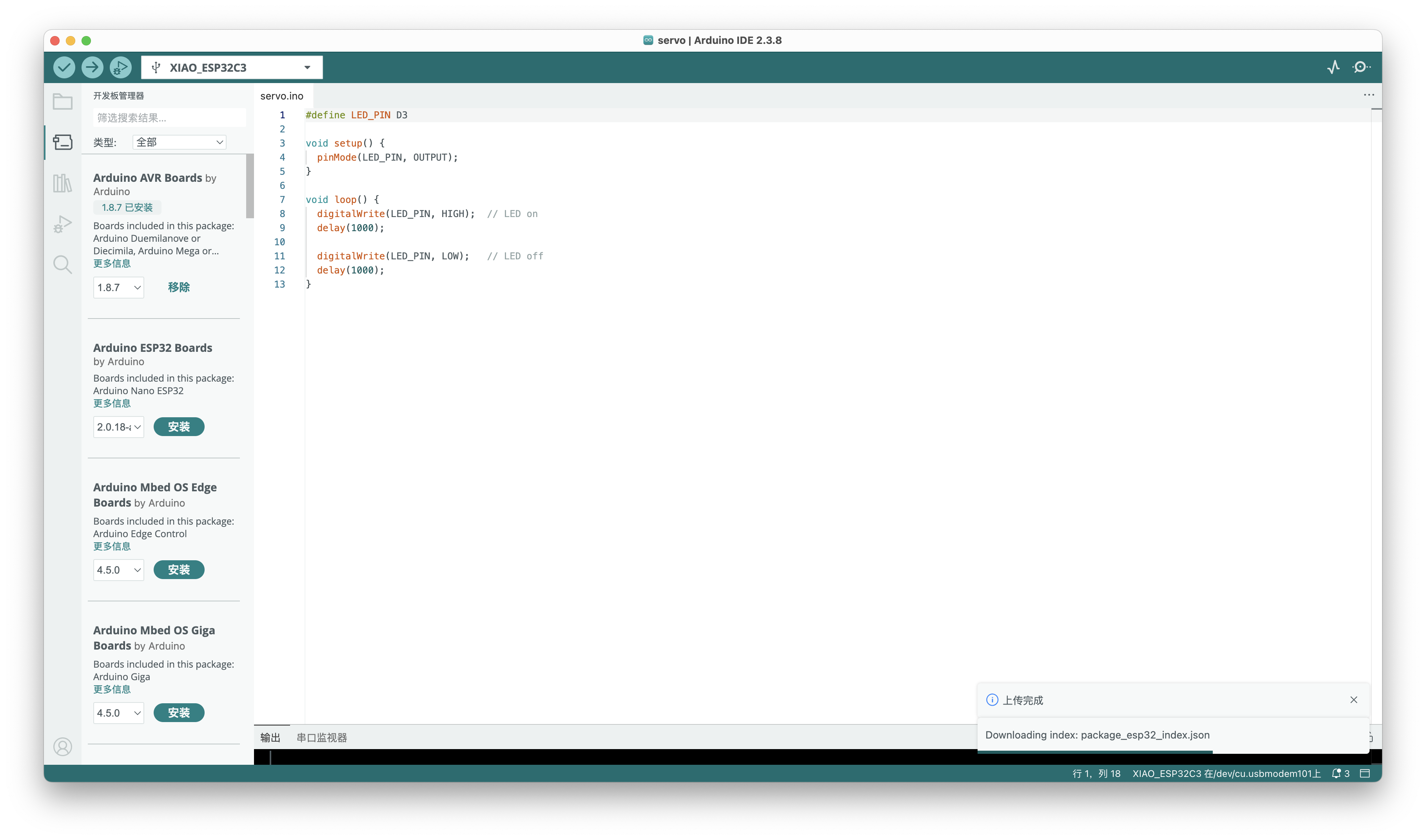
D3 LED Test
The first functional test was the onboard LED.
I used D3 because Arduino recognized this pin name.
#define LED_PIN D3

void setup() {
  pinMode(LED_PIN, OUTPUT);
}

void loop() {
  digitalWrite(LED_PIN, HIGH);
  delay(1000);

  digitalWrite(LED_PIN, LOW);
  delay(1000);
}Troubleshooting and Debugging
Debugging means finding and fixing problems in code and hardware.
My first issue was the pin name.
Arduino IDE did not recognize A3 for this board package.
The error message suggested D3 instead.
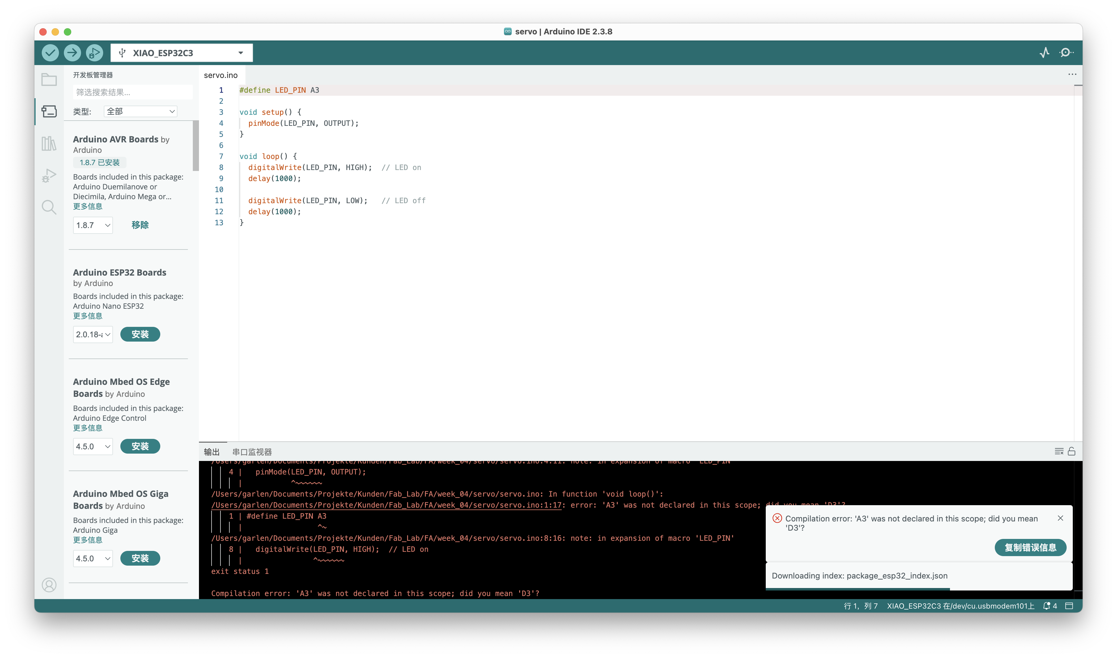
I changed the test code from A3 to D3.
I also checked the LED direction, resistor, D3 trace, and GND.
This showed that debugging needs both software and hardware checks.
Reflection
This week helped me understand PCB production as a complete workflow.
I moved from schematic design to a working physical board.
I learned that design rules depend on real machines and materials.
I also learned to debug step by step.
This board became a small platform for later embedded tests.
AI Use Statement
I used AI to organize my documentation structure.
AI helped me rewrite long notes into shorter English sentences.
AI also helped me check HTML consistency with other weekly pages.
AI helped me translate machine settings into English.
AI helped organize feedback about setup and deburring.
AI did not design the circuit or fabricate the PCB.
The design, milling, soldering, testing, and photos are my own work.