Overview
This week moved electronics design from theory into a real board. I also tested a real output signal.
My final project is an AI companion robot. So I did not want to make a generic practice board.
I used this week to build the first control board for the robot. It handles movement, input, feedback, and debugging.
Assignment Structure
| Part | What I Did |
|---|---|
| Group | We used test equipment to observe an embedded microcontroller output. |
| Individual | I designed a board for a XIAO ESP32C3 control system. |
Group Assignment
Observing an Embedded Microcontroller
We used lab equipment to observe a microcontroller output. This was more direct than only checking code.
We connected an ESP32-based board to an LED output. Then we probed the output pin with an oscilloscope.
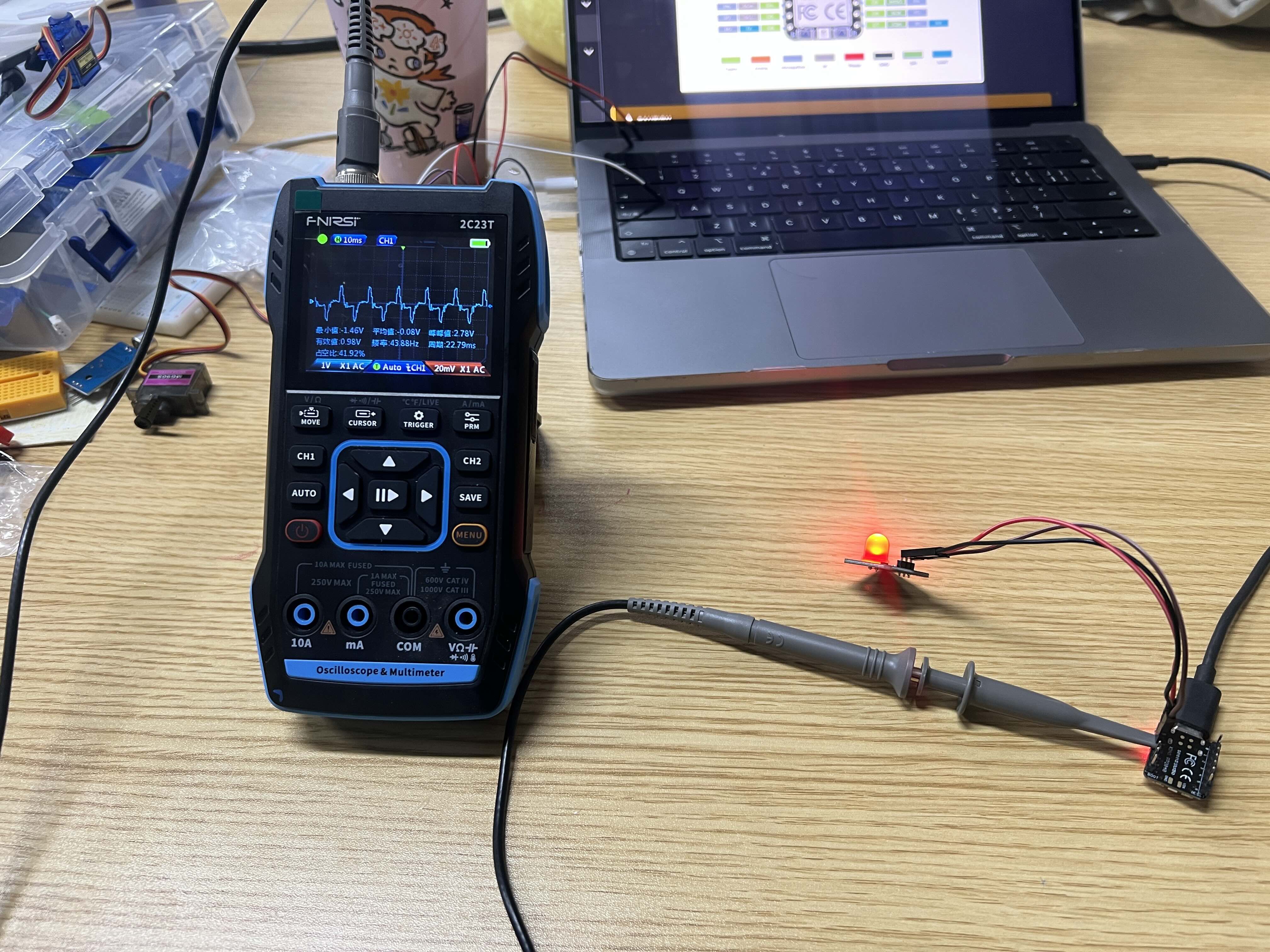
The waveform repeated steadily. The oscilloscope showed these approximate values.
- Frequency: about 50 Hz
- Period: about 20 ms
- Duty cycle: about 42%
This looked like a PWM-style signal. Seeing it directly helped me connect code with real voltage changes.
Individual Assignment
Designing a Control Board
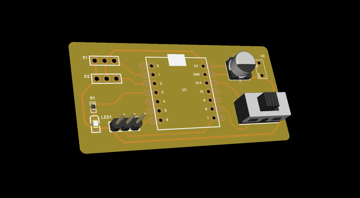
I designed the first electronics structure for my final project. The board supports the robot's physical control layer.
I kept this version simple. I wanted a board that could be milled and tested quickly.
System Breakdown
I separated the robot into a physical control layer and a media layer. This week focused on the ESP32C3 side.
Physical Control Layer (ESP32C3)
├ Servo L (Movement)
├ Servo R (Movement)
├ Slide Switch (User Input)
├ Status LED (Visual Feedback)
└ UART Debug (Communication)
This helped me avoid adding too much at once. I focused on movement, input, feedback, and debugging.
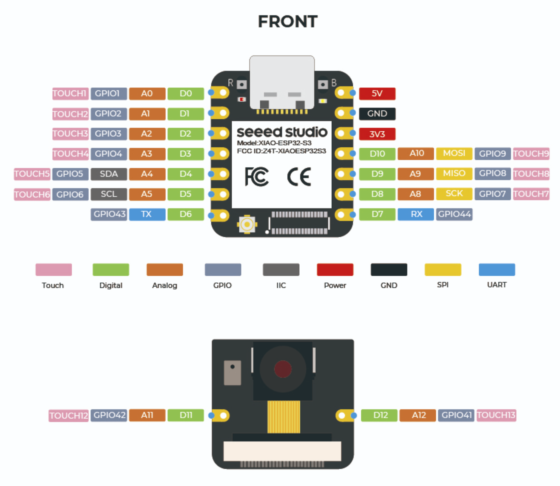
Why I Chose the XIAO ESP32C3
I chose the XIAO ESP32C3 because it is small and light. It also gives enough pins for this first board.
Its size fits a small robot body. It still supports basic control, input, and debugging.
EDA Tool Choice
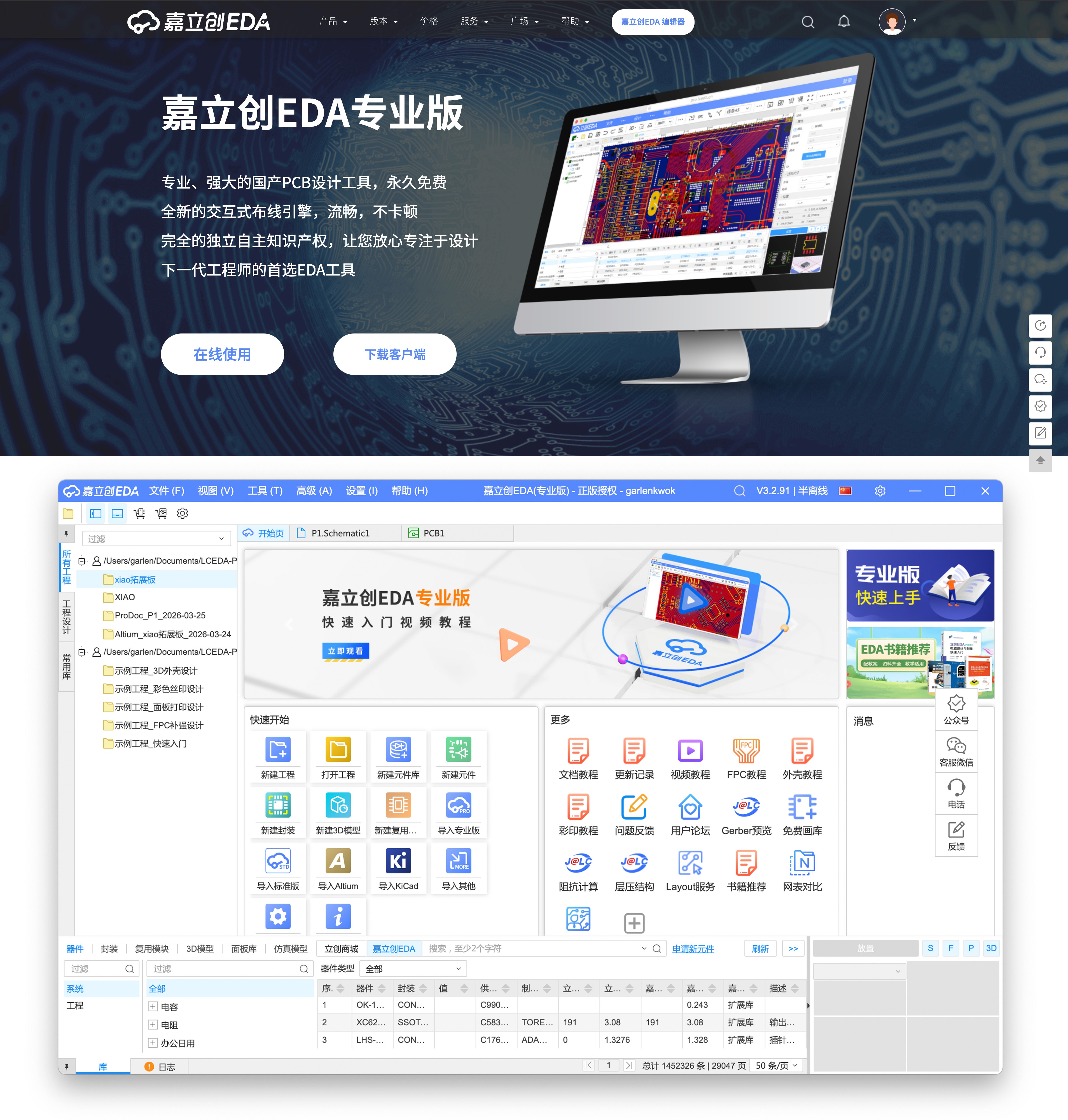
I used LCEDA Pro, also called EasyEDA Pro. I used it for schematic drawing and PCB layout.
I considered using KiCad, but LCEDA Pro matched my local workflow better for this board. I am working in China, so LCEDA Pro made component sourcing easier.
LCEDA Pro connects closely with Chinese component suppliers and online stores. This helped me search parts, check packages, and buy the same components later.
It also connects with JLCPCB services. This is useful for fast PCB prototyping, including free or low-cost trial fabrication options when available.
KiCad is still a powerful EDA tool. However, for this week, LCEDA Pro helped me move faster from component search to schematic, PCB layout, 3D preview, and future fabrication.
I downloaded LCEDA Pro from its official website: https://pro.lceda.cn/
EasyEDA / LCEDA Pro Workflow
This section shows how I made the board, not only the final result.
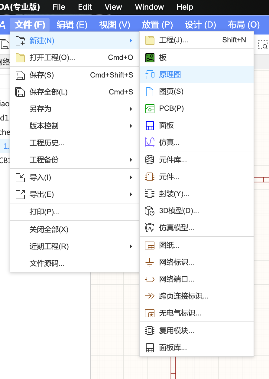
Create a New Schematic
I started with a new schematic document. I used File, New, and then Schematic.
Search for Components
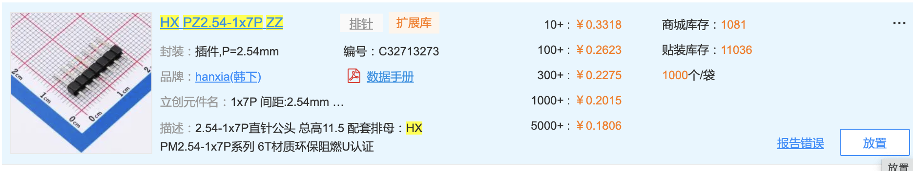
I pressed P to open the component and reuse window. Then I searched for the parts I needed.
I searched for headers, resistors, LEDs, servo connectors, and a slide switch.
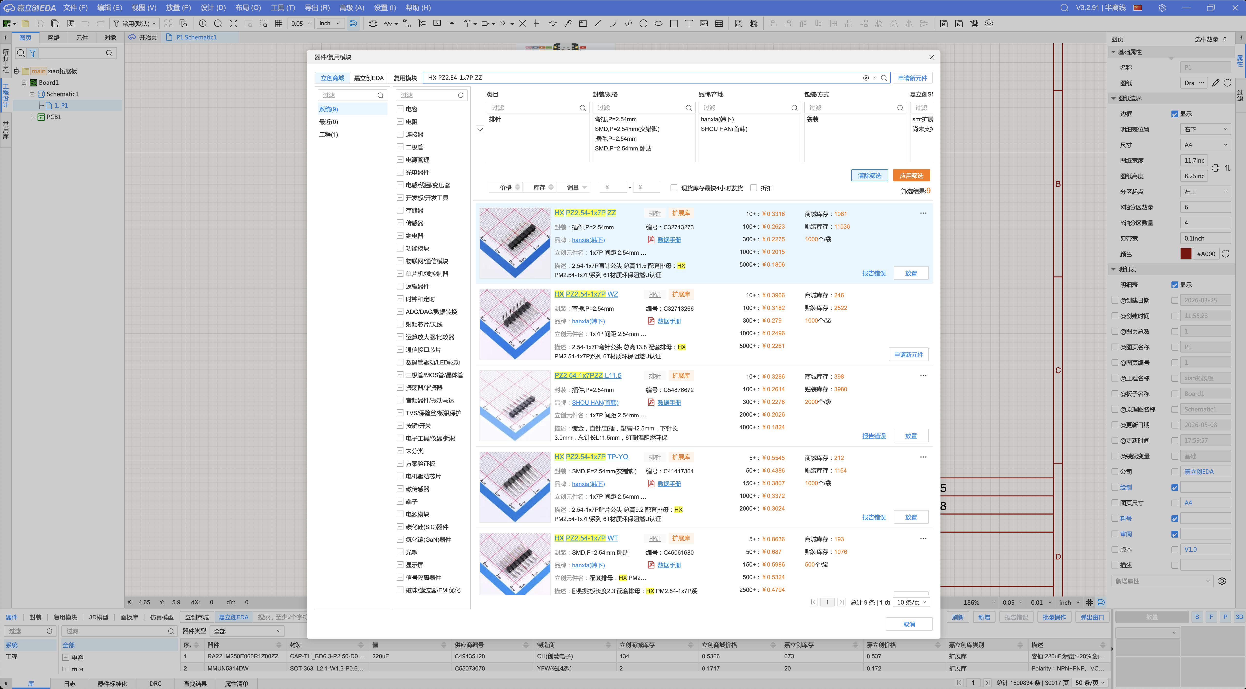
Place the Components
After choosing a part, I clicked Place. The part then followed my mouse on the schematic.
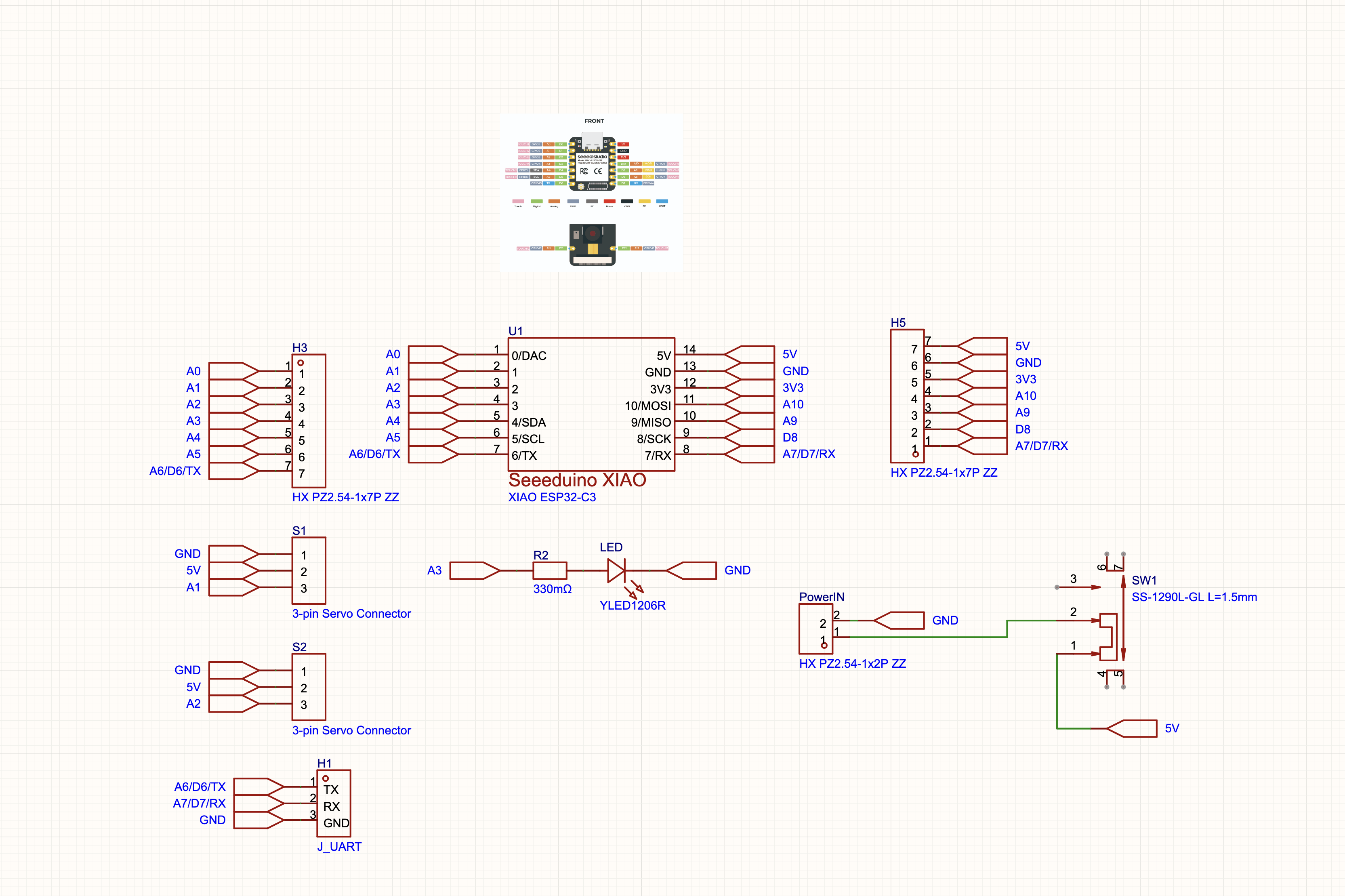
Import the XIAO ESP32C3 Resources
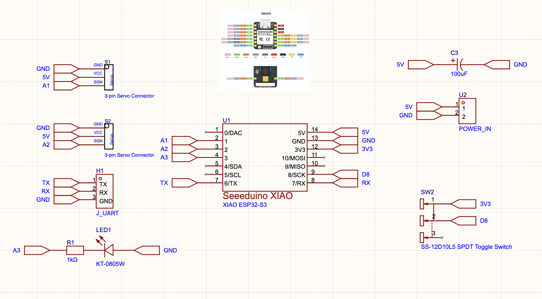
The XIAO ESP32C3 was not in my local EasyEDA library. So I used the official Seeed page.
I downloaded the KiCad project, symbols, footprints, and pinout sheet. Then I imported the needed files into LCEDA Pro. XIAO ESP32C3 official resources
Finish the Schematic
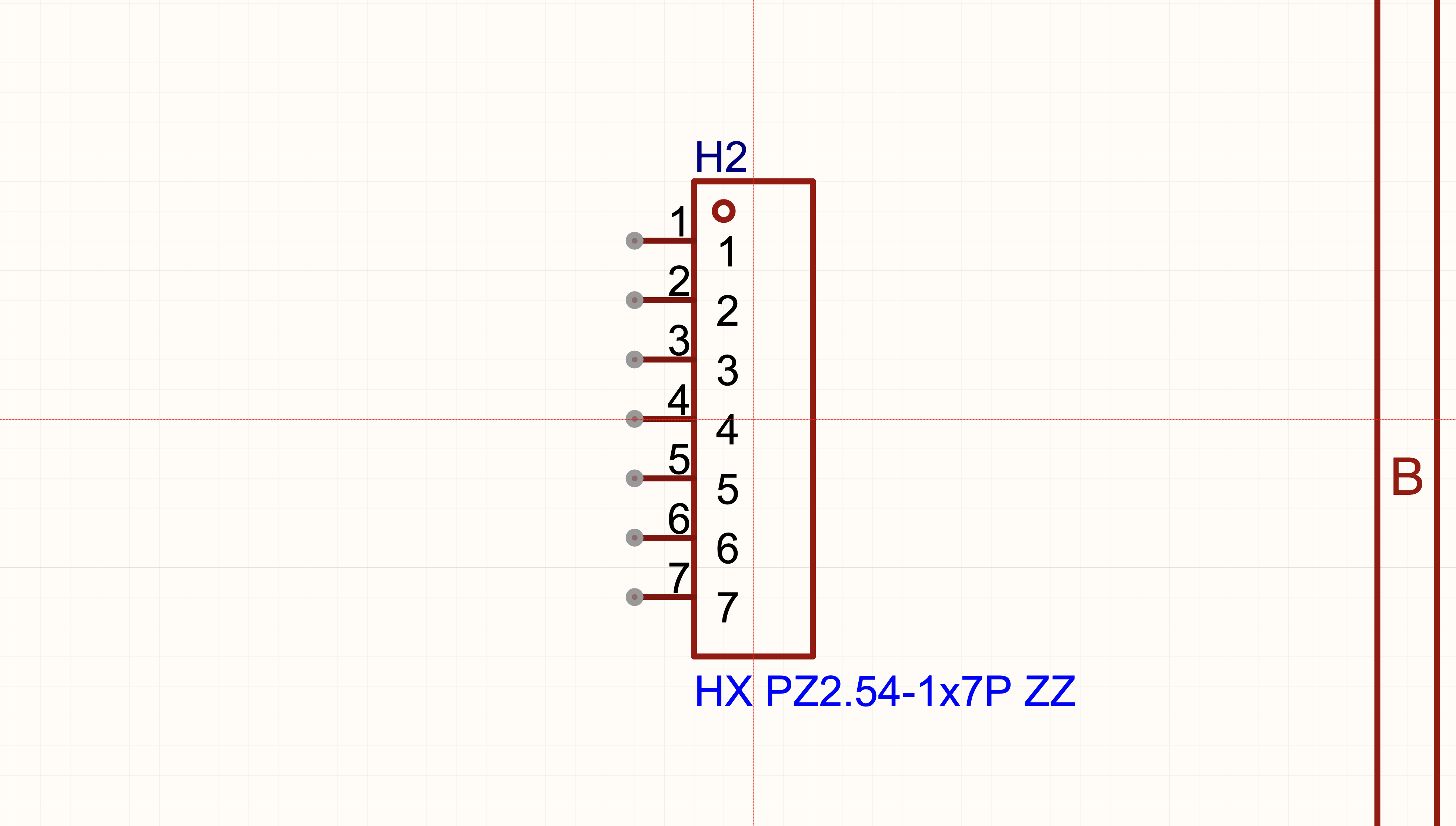
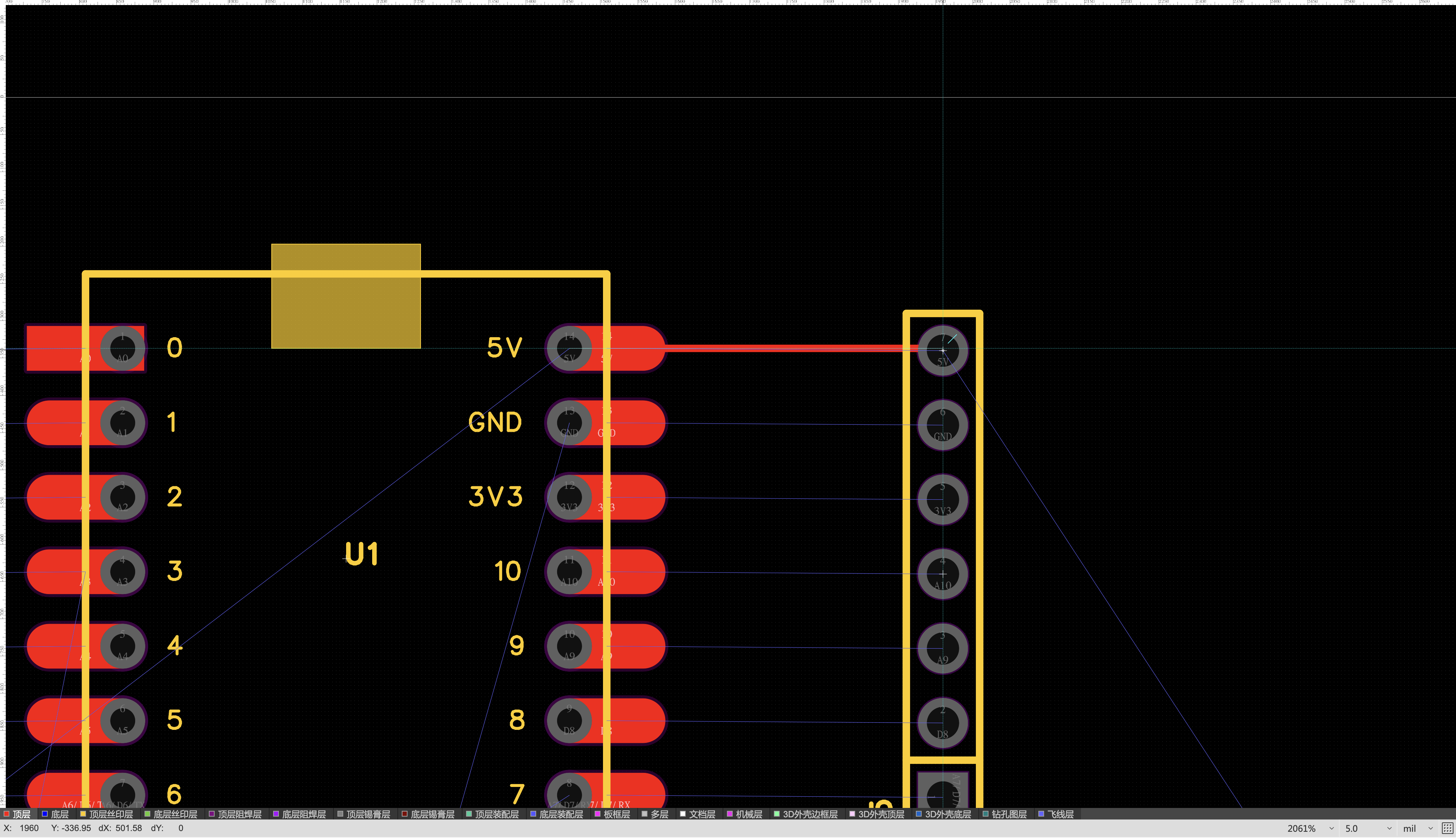
I connected each part based on my pin plan. Servo outputs used A1 and A2.
The LED used A3 with a 330 ohm resistor. I also added power, switch, and UART connections.
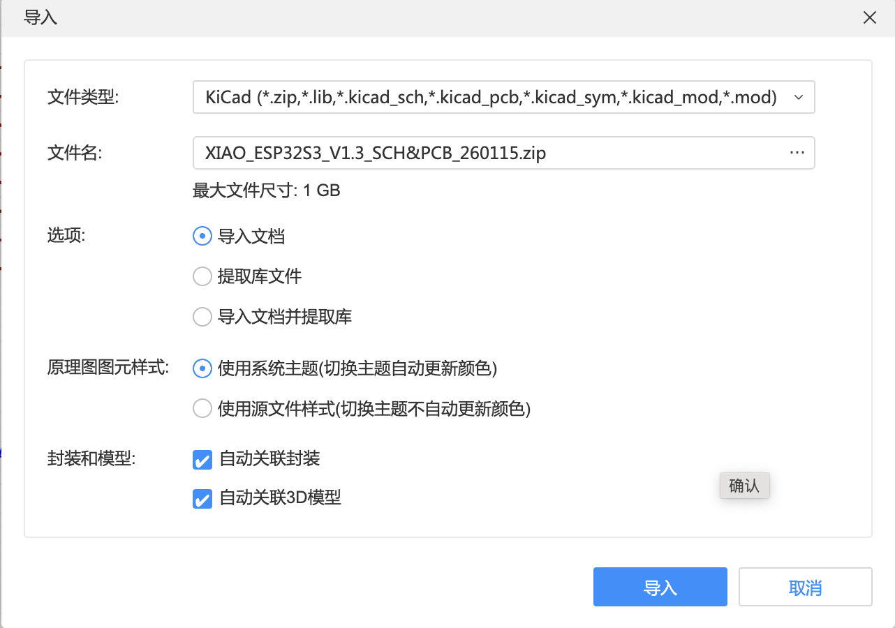
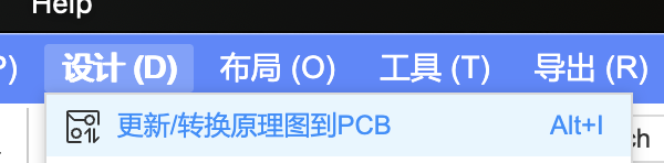
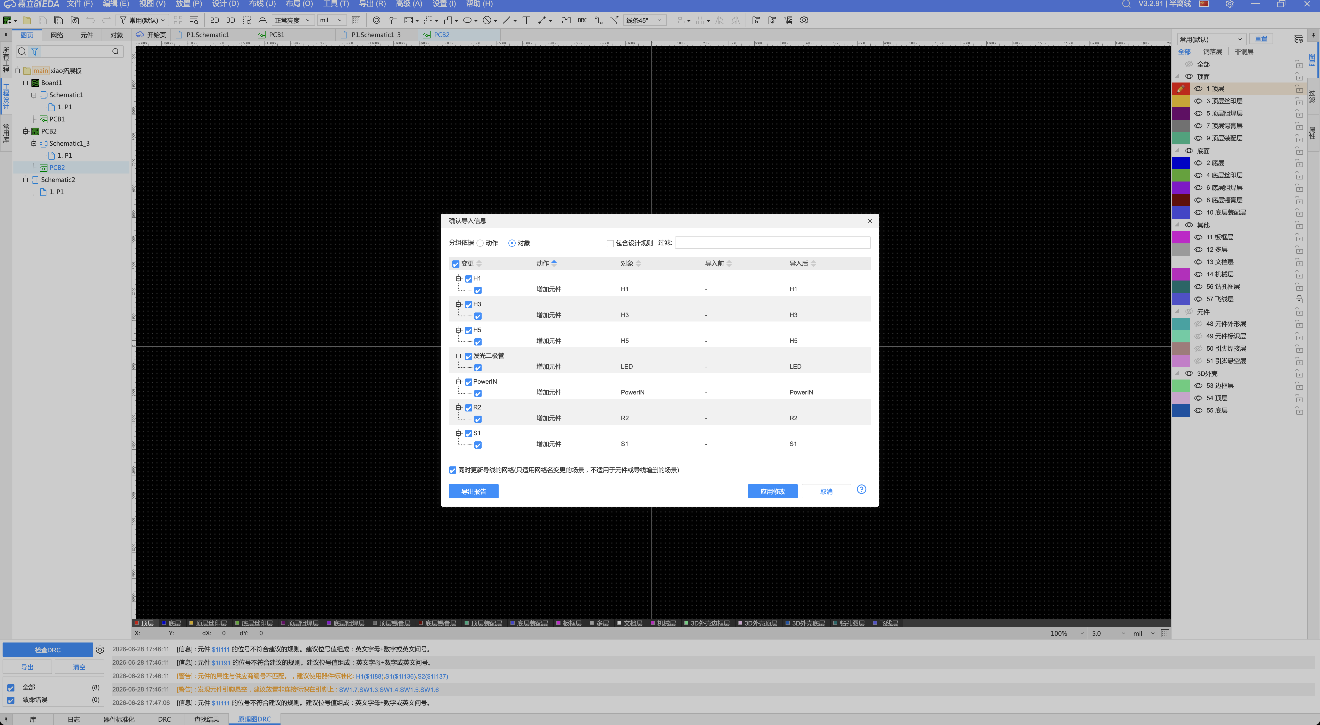
Convert the Schematic to PCB
After finishing the schematic, I converted it into a PCB. LCEDA Pro listed the imported objects.
I checked the components and net connections. Then I applied the update.
Arrange the Parts
The PCB first appeared with blue ratlines. These lines showed which pads needed connections.
I moved the parts into a clearer layout. This made routing easier.
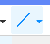
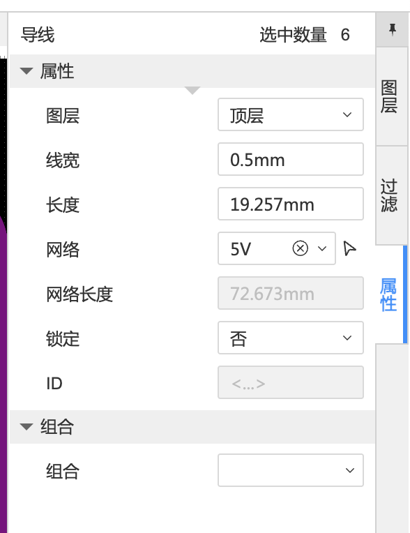
Route the Board
I used the routing tool to draw copper traces. I kept the traces on the top layer.
I set the trace width to 0.5 mm. This wider trace works better for CNC milling.
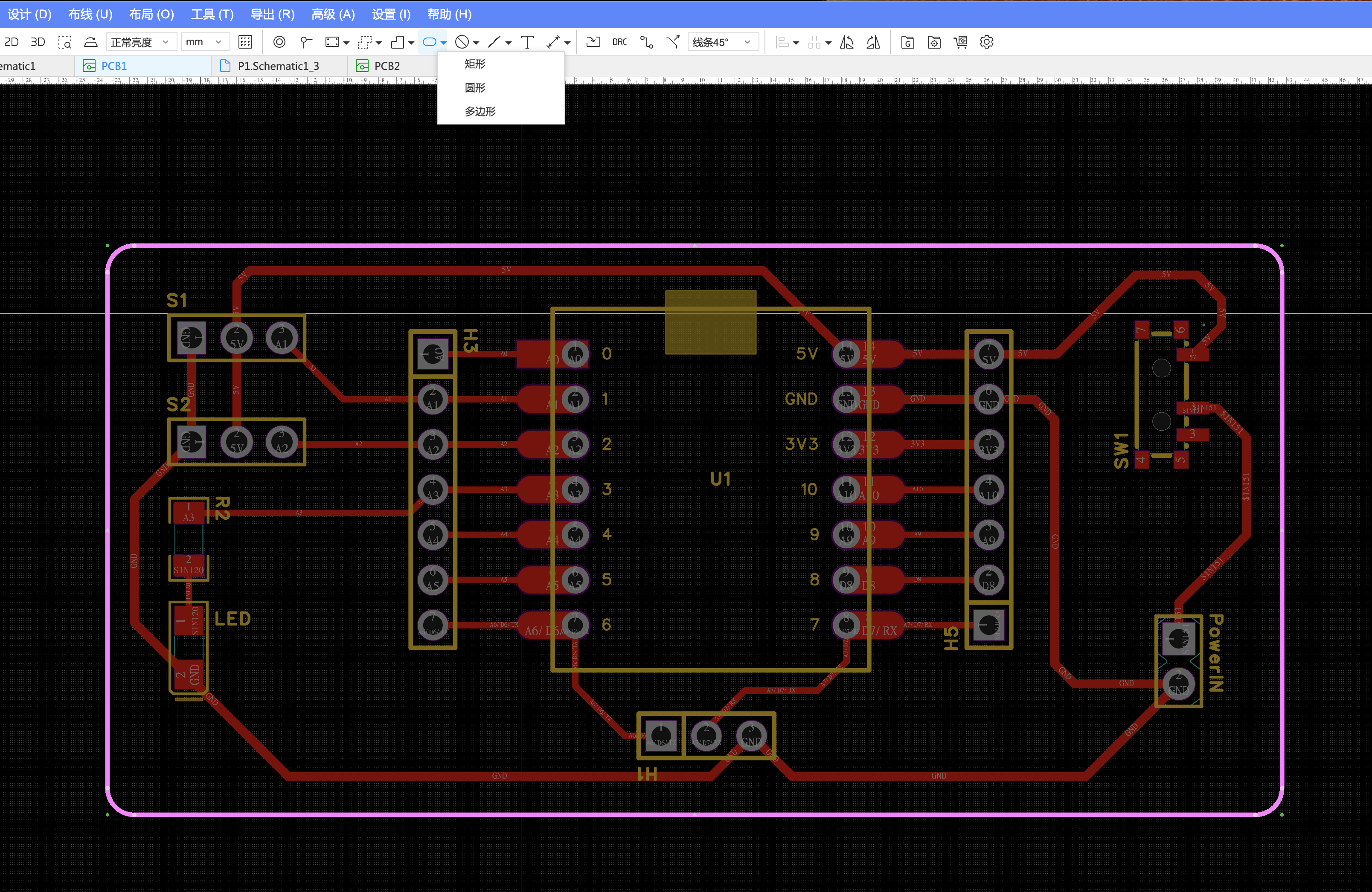
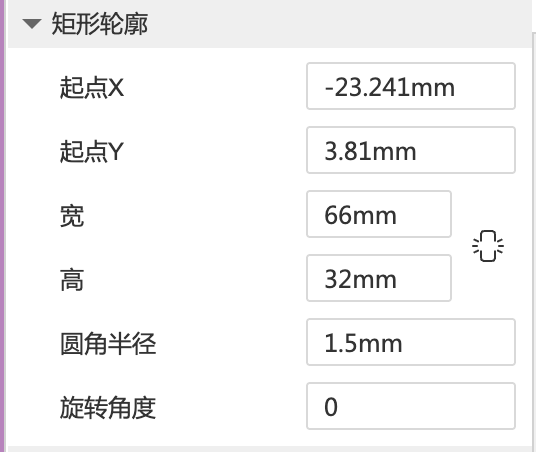
Draw the Board Outline
After routing, I drew the outer board outline. This outline defines the milling boundary.
Pin Planning
I mapped the main functions before drawing the schematic. This made the compact XIAO layout easier to manage.
| Function | Pin / Interface | Notes |
|---|---|---|
| Servo L | A1 | Left movement output |
| Servo R | A2 | Right movement output |
| Slide switch | D8 | User input and mode selection |
| Status LED | A3 | Visual feedback and debugging |
| UART TX/RX | Serial pins | Reserved for communication |
| Power input | 5V / GND | Main board power |
Schematic and BOM
The schematic used the XIAO ESP32C3 as the main controller. It included servo outputs, a switch, an LED, UART, and power.
Most common parts came from the EasyEDA library. I selected footprints that matched parts in the lab.
The status LED used a 330 ohm resistor. This keeps the LED current in a safe range.
| Designator | Component | Package / Footprint | Quantity |
|---|---|---|---|
| U1 | Seeed Studio XIAO ESP32C3 | SMD / through-hole hybrid | 1 |
| LED | Red LED | 1206 SMD | 1 |
| R2 | 330 ohm resistor | 1206 SMD | 1 |
| SW1 | Slide switch | Through-hole | 1 |
| S1, S2 | 3-pin servo connector | 2.54 mm through-hole | 2 |
| H3, H5 | 7-pin female header | 2.54 mm through-hole | 2 |
| H1 | 3-pin UART header | 2.54 mm through-hole | 1 |
| PowerIN | 2-pin header | 2.54 mm through-hole | 1 |
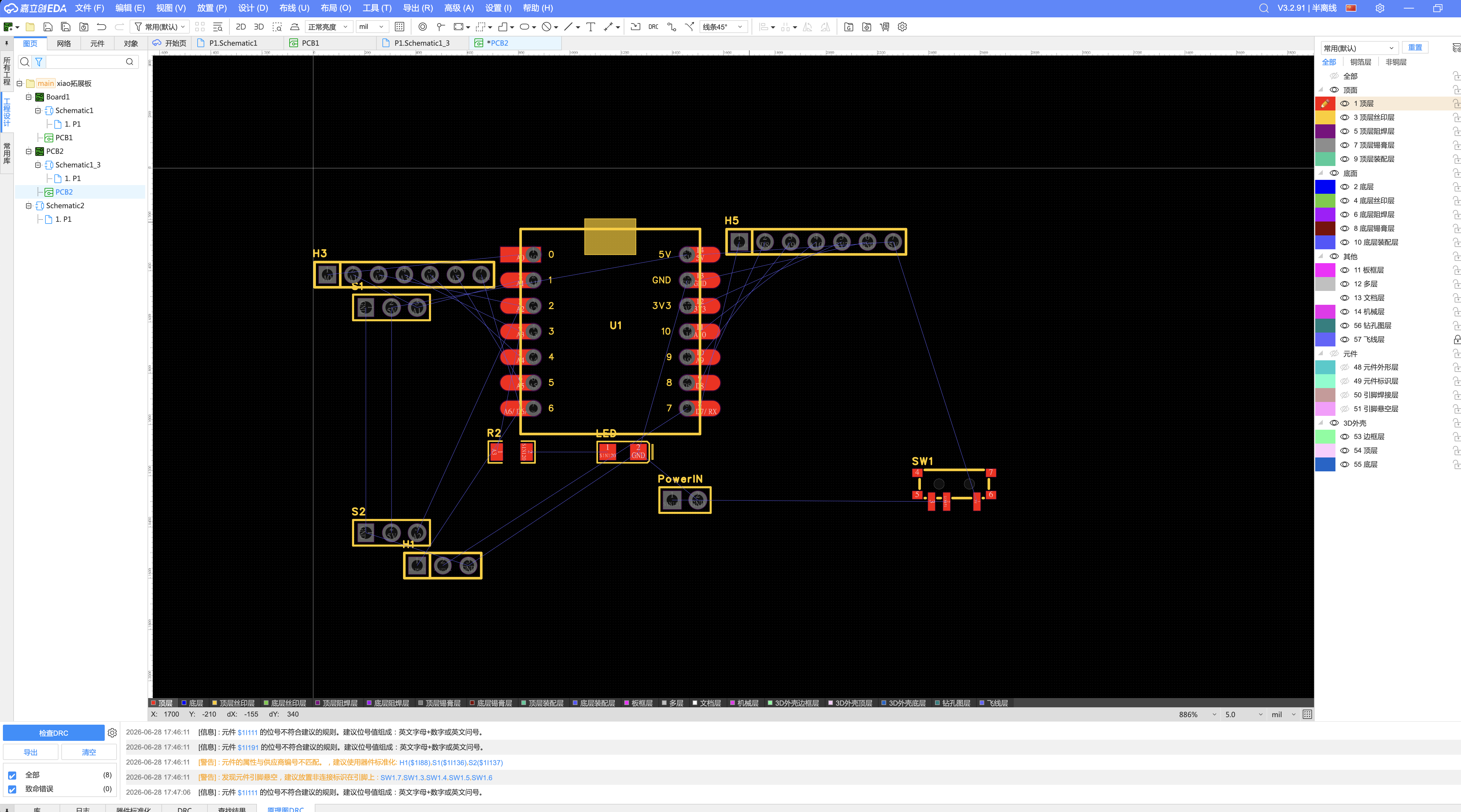
PCB Layout and DRC
I placed the XIAO module near the center. I arranged the connectors around it for easier wiring.
I routed the board with 0.5 mm traces. I used 45-degree turns and avoided sharp corners.
I kept the board single-sided. This made it easier to mill in the lab.
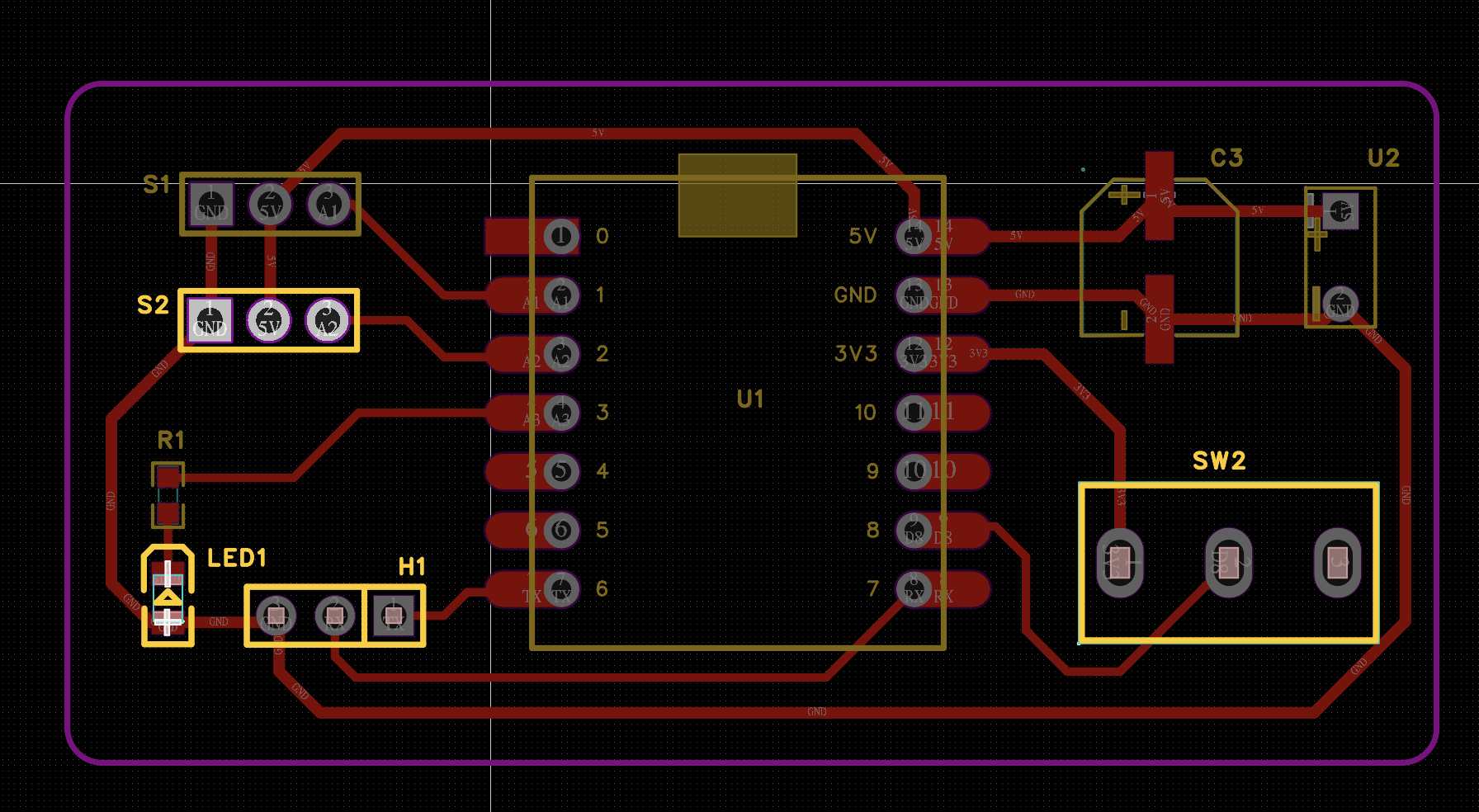
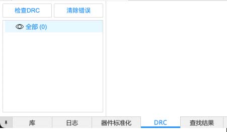
After routing, I ran the DRC tool. The final check showed zero design rule errors.
Reflection
This week helped me understand electronics as a real physical system. A signal is not only code.
The EasyEDA workflow also made PCB design feel more concrete. I could see each step from schematic to board.
The biggest lesson was scope control. A small working board is better than an overloaded first version.
Image Documentation Note
The images show my design process, not only final results. They document measurement, schematic design, routing, and checking.
group_setup.jpg: oscilloscope testing setup.group_waveform.mp4: measured output waveform.xiao_pinout.jpg: pinout reference for planning.easyeda_new_schematic_menu.png: new schematic setup.easyeda_component_library_search.png: component library search.easyeda_component_library_detail.png: component package check.xiao_esp32c3_official_resources.png: official resource page.easyeda_pcb_update_confirm.png: PCB import confirmation.easyeda_trace_width_0_5mm.png: trace width setup.easyeda_routed_board_with_outline.png: routed board with outline.week06_drc_result.jpg: final DRC result.
AI Use Statement
I used AI to organize the documentation and improve the English writing. I also used it to make the workflow clearer.
I made the circuit, schematic, PCB layout, trace settings, and DRC checks myself. I also made the screenshots and videos.
No AI-generated image is used as technical evidence here. All technical images are my own screenshots or camera records.