Week 16
Wildcard Week
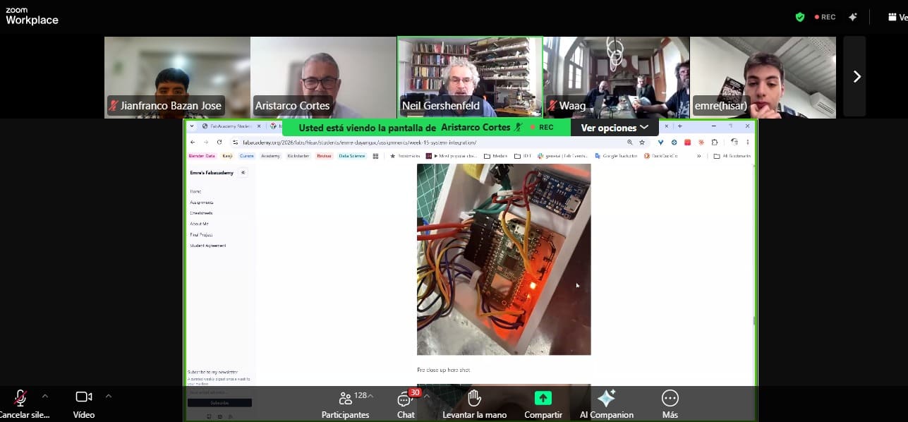
Class with Neil
During the Wildcard Week lecture with Neil, we explored how digital fabrication can go beyond the standard processes covered in previous assignments by experimenting with alternative manufacturing methods and creative workflows. The class focused on combining computer-aided design (CAD), digital manufacturing, electronics integration, and fabrication techniques to develop projects that expand our understanding of digital production. Neil emphasized the importance of documenting the complete workflow, including design decisions, fabrication parameters, machine settings, testing processes, and reproducibility.
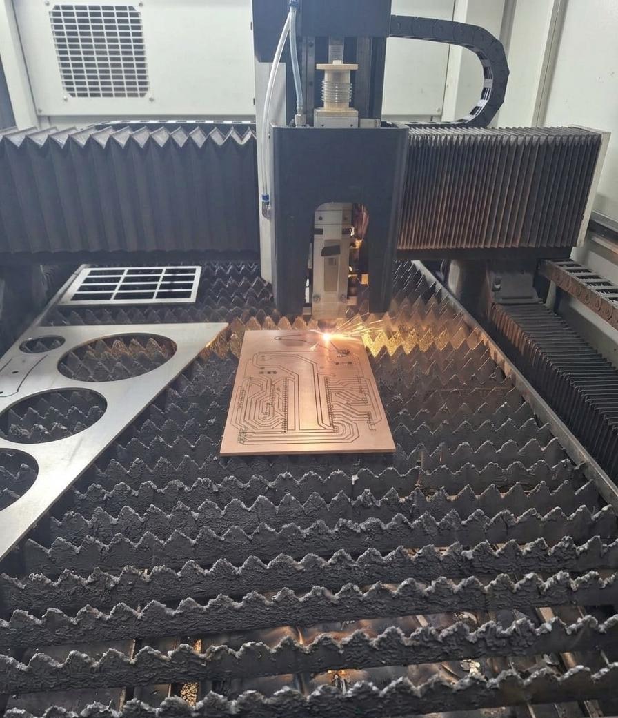
One of the key lessons from this week was understanding how different fabrication technologies can be adapted for unconventional applications. Inspired by this approach, I explored the use of a fiber laser cutting machine to manufacture a PCB using baquelite material, applying different laser parameters for copper engraving and board cutting. This assignment helped me better understand how experimentation, problem-solving, and digital manufacturing flexibility are essential parts of the prototyping and product development process within Fab Academy.
Have you answered these questions?
- I.Documented the workflow(s) and process(es) you used✅
- II.Explained how your process is not covered in other assignments ✅
- III.Described problems encountered (if any) and how you fixed them ✅
- IV. Included original design files and source code✅
- V. Included ‘hero shot’ of the result ✅
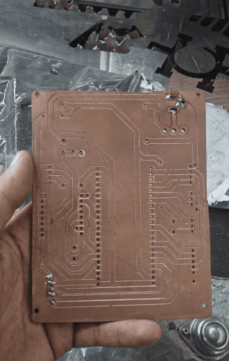
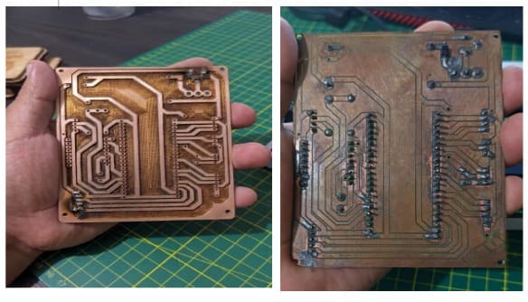
1. Hero Shot
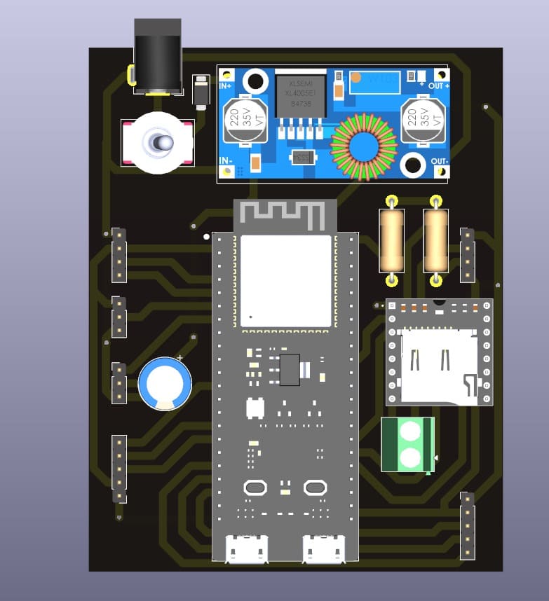
This hero shot represents the final result of my Wildcard Week assignment, where I combined digital fabrication, electronics integration, and computer-aided manufacturing into a single functional prototype. The project focuses on the development of a custom electronic control system using an ESP32 S3 Dev Kit, a power regulation module, and an MP3 audio system integrated into a fabricated enclosure and support structure. The final prototype demonstrates how digital processes can be combined to create a more complete and product-oriented electronic system.
Through this assignment, I explored fabrication methods that were not fully covered in previous assignments, especially the integration of customized electronic packaging, structural assembly, and advanced digital manufacturing workflows. This project allowed me to improve my understanding of system organization, component integration, and the relationship between CAD design and real-world fabrication processes.
2. Introduction
Wildcard Week allowed me to experiment with a digital fabrication process outside the standard assignments covered during Fab Academy. For this project, I focused on integrating electronics, structural fabrication, and customized packaging into a single system capable of powering and controlling multiple electronic modules. The project combines CAD modeling, PCB integration, digital fabrication, and assembly techniques to create a functional embedded device.
The system includes an ESP32 S3 Dev Kit CN 16R8 as the main controller, a power regulation system using the XL4005 buck converter, an MP3 audio module with a speaker, and several protection and connection components such as Schottky diodes, capacitors, terminal blocks, switches, and female headers. All components were organized to create a compact and functional electronic platform.
📈3. Digital Fabrication Workflow
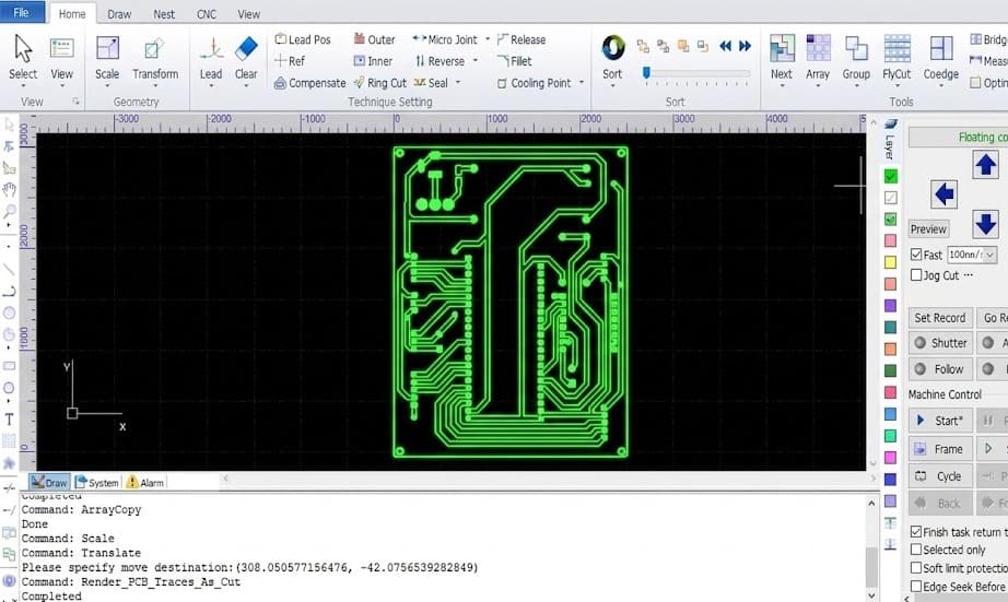
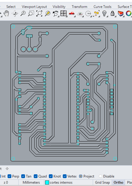
The digital fabrication workflow of this project was focused on the use of a fiber laser cutting machine to manufacture the PCB using a baquelite copper board. The process started with the PCB design prepared in CAD and PCB software, where the electronic traces and cutting boundaries were exported for fabrication. After preparing the design files, the PCB layout was imported into the laser machine software to configure the engraving and cutting operations according to the material dimensions and fabrication requirements.
Two different parameter configurations were used during the manufacturing process. The first configuration was dedicated to the engraving/desbaste process, where the fiber laser removed the copper layer from the baquelite board to generate the conductive traces and electronic pathways. The second configuration was used for the cutting stage, where the external contour of the PCB was precisely cut to separate the final board from the material sheet. This workflow allowed the PCB to be fabricated using a non-traditional digital manufacturing process different from the standard milling methods used in other assignments.
Raster Parameters – PCB Engraving (Baquelite)
| ⚙️ Parameter | 📌 Value | 📝 Description |
|---|---|---|
| Process Type | Raster / Engraving | Used to remove the copper layer from the PCB surface. |
| Material | Baquelite PCB | Copper-clad phenolic board. |
| Laser Power | 20 – 35% | Low-medium power to avoid damaging the substrate. |
| Speed | 1500 – 2500 mm/s | Controls engraving precision and copper removal. |
| Frequency | 20 – 40 kHz | Pulse frequency for stable engraving. |
| Line Spacing | 0.03 – 0.05 mm | Determines engraving density and detail quality. |
| Passes | 1 – 2 Passes | Additional passes improve copper removal. |
| Focus | Auto / Manual Focus | Important for accurate trace engraving. |
| Cooling | Air Assist Recommended | Helps reduce smoke and overheating. |
Cutting Parameters – External PCB Contour
| ⚙️ Parameter | 📌 Value | 📝 Description |
|---|---|---|
| Process Type | Vector Cut | Used for cutting the external PCB shape. |
| Material | Baquelite PCB | Phenolic board with copper layer. |
| Laser Power | 60 – 80% | Higher power required for full material cutting. |
| Speed | 300 – 800 mm/s | Lower speed improves cutting depth. |
| Frequency | 20 – 50 kHz | Optimized for cleaner edge cutting. |
| Passes | 2 – 4 Passes | Multiple passes ensure complete cutting. |
| Cut Direction | Outside Cut | Maintains accurate PCB dimensions. |
| Focus | Precise Surface Focus | Essential for clean contour edges. |
| Material Fixing | Double-sided Tape / Clamps | Prevents PCB movement during cutting. |
⚙️4. CAD Design and System Planning
The CAD stage played an important role in the success of the project because it allowed me to visualize the complete system before fabrication. During the design process, I organized the internal layout to optimize cable routing, power distribution, ventilation, and accessibility to connectors and switches. Special attention was given to the positioning of the power jack, ON-OFF-ON switch, and female headers to simplify future modifications and maintenance.
The design also considered the physical dimensions of each electronic module, ensuring enough space for the XL4005 buck converter, capacitors, ESP32 S3 board, and MP3 module with speaker output. By using CAD planning before fabrication, I minimized assembly problems and improved the final appearance of the project, making the system look cleaner and more professional.
5. Electronic Components Integration
The electronic system was designed around the ESP32 S3 Dev Kit CN 16R8, which acts as the main microcontroller responsible for system control and future communication features. To provide stable power to the entire system, I integrated an XL4005 DC-DC buck converter capable of regulating voltage efficiently. Additional components such as the 100uF capacitor and SS34 Schottky diode were added to improve voltage stability and protect the circuit from reverse polarity issues.
The MP3 module and speaker were integrated as the main output devices, allowing the system to reproduce audio signals controlled by the ESP32. Female header connectors were also added to facilitate the integration of future input and output modules. This modular approach makes the system more flexible and scalable for future project improvements.
6. Manufacturing Process
The manufacturing process combined PCB digital design with fiber laser fabrication technology to produce the final electronic board. After completing the PCB layout design, the fabrication files were prepared and transferred to the fiber laser cutting machine. The baquelite board was carefully positioned on the machine bed to ensure proper alignment before starting the engraving process. Special attention was given to the calibration of the laser focus and material positioning to achieve precise copper removal.
Different machine settings were applied depending on the fabrication stage. Lower power and controlled speed parameters were used during the copper engraving process to avoid damaging the substrate while accurately removing the conductive layer. After completing the engraving operation, a second laser configuration with stronger cutting parameters was used to cut the external PCB shape. This method demonstrated how fiber laser technology can also be integrated into PCB prototyping and digital manufacturing workflows..
7. Why This Process is Different from Other Assignments
This project differs from previous assignments because the PCB fabrication was performed using a fiber laser cutting machine instead of traditional PCB milling or CNC engraving methods commonly used in Fab Academy. The process required configuring laser parameters specifically for copper engraving and baquelite cutting, introducing a different manufacturing workflow focused on laser-material interaction rather than mechanical machining.
Additionally, this fabrication approach combines precision laser engraving with electronic manufacturing, which is not typically covered in other assignments. The use of separate parameter configurations for copper desbaste and external contour cutting allowed me to explore alternative PCB fabrication techniques while improving my understanding of digital manufacturing processes and material behavior during laser processing.
8. Problems Encountered and Solutions
One of the main challenges during the project was organizing all electronic components inside the enclosure while maintaining proper cable management and airflow. Initially, some components occupied too much internal space, making assembly difficult. To solve this issue, I modified the internal CAD layout and reorganized the placement of the voltage regulator and connectors to optimize the available area.
Another difficulty involved stabilizing the power distribution between the ESP32, MP3 module, and speaker system. During early testing, voltage fluctuations occasionally affected audio performance. To improve stability, I added filtering capacitors and optimized the grounding connections. After these modifications, the system operated more reliably and maintained stable audio playback.
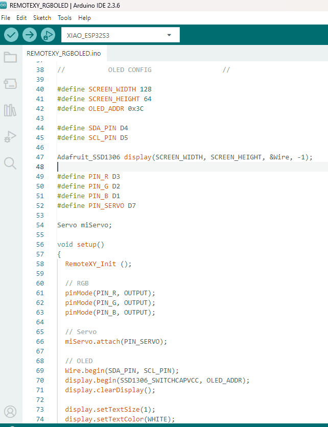
9. Original Design Files and Source Code
To ensure reproducibility of the project, all original design files and source code were properly organized and documented. This includes CAD design files, PCB schematics, fabrication files, and embedded programming code used for the ESP32 S3 microcontroller. These files allow the project to be reproduced, modified, or expanded in future iterations.
The source code controls the initialization of the system, power behavior, and communication between the ESP32 and the MP3 module. Keeping all files organized was essential for simplifying debugging, future upgrades, and system maintenance while also meeting the documentation requirements of Fab Academy.
10. Individual Reflection
This assignment helped me understand how different areas of digital fabrication can be combined into a single integrated system. Throughout the process, I improved my skills in CAD design, electronics integration, power management, and product-oriented fabrication. I also learned the importance of planning component placement, cable routing, and enclosure design before starting the manufacturing stage.
Wildcard Week was especially valuable because it allowed me to explore fabrication techniques and integration strategies beyond the standard assignments. By combining embedded electronics, digital manufacturing, and packaging concepts into one project, I gained a deeper understanding of how complete electronic products are developed from concept to final prototype.
Files
Here are the project files available for download:
- Design in DXF: Download .ino
- Design in Dwg: Download .ino